
Low-Cost Shadow Mask Fabrication for Nanoelectronics


1
Materials Science Factory, Instituto de Ciencia de Materiales de Madrid (ICMM-CSIC), E-28049 Madrid, Spain
2
Departamento de Física de la Materia Condensada, Universidad Autónoma de Madrid, E-28049 Madrid, Spain
*
Authors to whom correspondence should be addressed.
Nanomanufacturing 2023, 3(3), 347-355; https://doi.org/10.3390/nanomanufacturing3030022
Submission received: 3 July 2023
/
Revised: 2 August 2023
/
Accepted: 8 August 2023
/
Published: 16 August 2023
Abstract
:We present two approaches for fabricating shadow masks for the evaporation of electrodes onto nanomaterials. In the first one, we combine the use of a commercial fiber laser engraving system with readily available aluminum foil. This method is suitable for fabricating shadow masks with line widths of 50 µm and minimum feature separation of 20 µm, and using it to create masks with complex patterns is very straightforward. In the second approach, we use a commercially available vinyl cutting machine to pattern a vinyl stencil mask, and we use a glass fiber to define the separation between the electrodes. With this approach, we achieve well-defined electrodes separated by 15 µm, but this technique is less versatile in creating complex masks as compared with the laser-based one. We demonstrate the potential of these techniques by fabricating field-effect transistor devices based on MoS2. Our approach is a cost-effective and easily accessible method for fabricating shadow masks with high resolution and accuracy, making it accessible to a wider range of laboratories.
1. Introduction
Electrode deposition is a critical step in the fabrication of electronic devices with nanomaterials. The most widely extended method to deposit electrodes is probably based on lithographic techniques, i.e., photolithography or electron beam lithography, which require specialized and expensive facilities as well as a strong technical background in micro-fabrication. Recent works show different approaches for lower-cost lithography setups used with nanomaterials [1,2]. Nevertheless, these lithographic techniques require chemical treatment steps to ensure the adhesion of the resists for the development and lift-off steps, which can harm certain nanomaterials that are more sensitive to the environment.
Direct metal evaporation through a shadow mask, on the other hand, has several advantages over conventional lithographic techniques [3,4,5,6]. For example, it is relatively inexpensive, easy to implement, and does not require a clean room environment. Additionally, it can be easily applied in labs that do not have a background or infrastructure in microfabrication. Another important aspect of the method is the fact that it is an ‘all-dry’ process, which means that it is also compatible with nanomaterials that tend to degrade or damage during the chemical and optical treatments involved in lithographic techniques [7,8,9]. Pre-patterned electrodes have the advantage of enabling a nanomaterial assembly in the glove box, which is crucial for air-sensitive materials [10,11].
Typically, shadow mask fabrication requires a specialized facility similar to those used for lithographic processing, which can be very costly [12,13]. Most research groups using shadow mask deposition buy commercially available masks or outsource the fabrication to micro-fabrication foundries, making the use of shadow mask deposition less flexible and unsuitable for rapid prototyping. This raises the question of whether there is a technique to fabricate shadow masks in a way that is affordable and flexible, which would allow research groups to design and fabricate their own customized masks without the need for costly infrastructure or fabrication outsourcing.
Tomczyk et al. recently published a work about laser ablation fabrication of masks using homebuilt optical systems. However, these systems were typically composed of expensive components, and the resolution achieved was only in the 50 to 100 µm range [14]. This may not be sufficient for many applications with nanomaterials, which require electrodes in the 10–50 µm range. Moreover, the reported laser ablation setups are difficult to use and expensive to implement, making it not suitable for many research groups. Elhami Nik et al. also reported a recent work about the use of a CO2 laser to ablate filter paper to create shadow masks, resulting in masks with a minimum feature size of 100 µm [15].
In this work, we present two approaches for fabricating shadow masks for the evaporation of electrodes to fabricate devices with nanomaterials, bridging the gap between flexibility in realizing the design and the cost factor. In the first method, we make use of a commercially available fiber laser engraving system (Atomstack M4, costing less than EUR 1100) with readily available metal supports (standard kitchen aluminum foil and thick aluminum foil) for shadow mask engraving of self-drafted layouts with maximum flexibility. In the second method, we use a vinyl cutting machine (Cricut Maker 3, under EUR 500) to create a vinyl stencil mask defining the electrodes and pads with pre-defined gap sizes and maximum cost-effectiveness. As the resolution of the vinyl cutter does not allow us to achieve electrode separation under 100 µm, we place a glass fiber (15 µm in diameter) to define the separation between the electrodes. We illustrate the potential of these methods by fabricating single-layer MoS2 field-effect transistors.
2. Materials and Methods
Figure 1a shows a picture of the compact fiber laser engraving system used in this work while it cuts through aluminum foil. The system uses a pulsed IR laser (1064 nm) focused on a spot of ~20 µm and features two scanning galvanometer mirrors that allow it to reach a marking speed of up to 12 m/s. We found that standard kitchen aluminum foil can be used to fabricate well-defined shadow masks, but handling them without creating folds/wrinkles can be challenging (note that an example of a kitchen aluminum foil mask is given in the Supporting Information Figure S1). We thus tested thicker aluminum foil (40 µm thick, 150 × 150 mm sheets, typically commercialized for use in shisha/hookah, LINK) that leads to optimal performance in terms of easiness to pattern and handle afterward. Figure 1b shows a picture of one of these thick aluminum foils, laser-cut to form a shadow mask with pads and drain-source electrodes separated by different gap sides, adhered to a SiO2/Si substrate with Kapton tape prior to metal evaporation. The inset in the figure shows a higher magnification image of one of the 20 µm gaps. We found that masks designed with a drain-source separation under 20 µm tend to fail, thus leading to a shorted drain-source connection.
Figure 1c shows a picture of the other system tested to fabricate inexpensive homemade shadow masks: a vinyl cutter. The system operates very similarly to an old-fashioned XY plotter system, but uses a sharp blade tool instead of a pen. This kind of system, although inexpensive and very easy to use, cannot be used to make small features or structures with small pitch (that is, below a 200 µm feature or pitch size, the vinyl-cut masks are not reliable). To fabricate shadow masks with a smaller separation between drain and source electrodes, we combined the vinyl-cut mask with a glass fiber that is 15 µm in diameter to define the separation between drain and source electrodes without being limited by the vinyl-cutting system. Previous works using glass or carbon fibers as shadow masks have been reported in the literature to provide good-quality electrodes [16,17]. The combination with a vinyl cut mask can provide a more controlled way to deposit the metal electrodes and to pattern the pads and the leads to avoid shorts with other parts of the device or with the back gate. Figure 1d shows an optical image of one of the vinyl cut masks where one can appreciate the pads and the electrode leads. One can also notice the glass fiber deposited in the central part of the substrate before adhering to the vinyl cut mask to define the drain-source separation. The inset shows a higher magnification image of the glass fiber, creating the separation between the electrodes.
3. Results
3.1. Fabrication of Electrodes by Metal Deposition through the Masks
In the following, we characterize the electrodes achieved after metal deposition through the shadow masks. We employ an electron beam evaporation system to deposit 5 nm of Ti (adhesion layer) and 45 nm of Au. Figure 2a shows an optical image of a shadow mask fabricated onto the 40 µm thick aluminum foil by laser ablation. Figure 2b shows an optical image of a SiO2/Si substrate after metal deposition that closely follows the shape of the shadow mask shown in Figure 2a. The inset in Figure 2b shows a higher magnification optical microscopy image of the gap between the drain and source electrodes. Figure 2c shows an optical image of a mask made with the combination of a glass fiber and a vinyl cut stencil. The mask is adhered onto a SiO2/Si substrate before metal deposition. Figure 2d is an optical image of the SiO2/Si substrate after metal deposition. The inset in 2d depicts a detail of the gap created between the drain and source with the glass fiber.
As one can clearly see from Figure 2, we found that the vinyl + glass fiber approach yields very well-defined drain-source electrodes whose separation is directly defined by the diameter of the fiber. But, this technique suffers from lower flexibility in exploring different customized electrode designs. The laser engraving method, on the other hand, yields poorly defined electrode edges but ensures complete flexibility over the pattern design. This increased flexibility allows for the design and implementation of new patterns and layouts, providing more freedom in the design process and enabling more advanced electronic devices to be fabricated with nanomaterials. Additionally, this method can be used to quickly test different designs, which will allow for faster development and optimization of the fabrication process. In this way, the use of a commercially available fiber laser engraving system can open the door to additional flexibility in shadow mask fabrication, providing a powerful tool for researchers working in the field of nanoelectronics, whereas the use of a vinyl cutter in combination with glass fibers can provide the most cost-effective route to fabricate devices for research groups running under a moderate budget. We direct the reader to Figure S2 in the Supporting Information for an atomic force microscopy (AFM) characterization of the electrodes fabricated with these shadow masks as well as with a commercially available shadow mask (Ossila E321, Ossila Ltd., Solpro Business Park, Windsor Street, Sheffield S4 7WB, UK).
3.2. Example of Devices Fabricated with the Shadow Masks
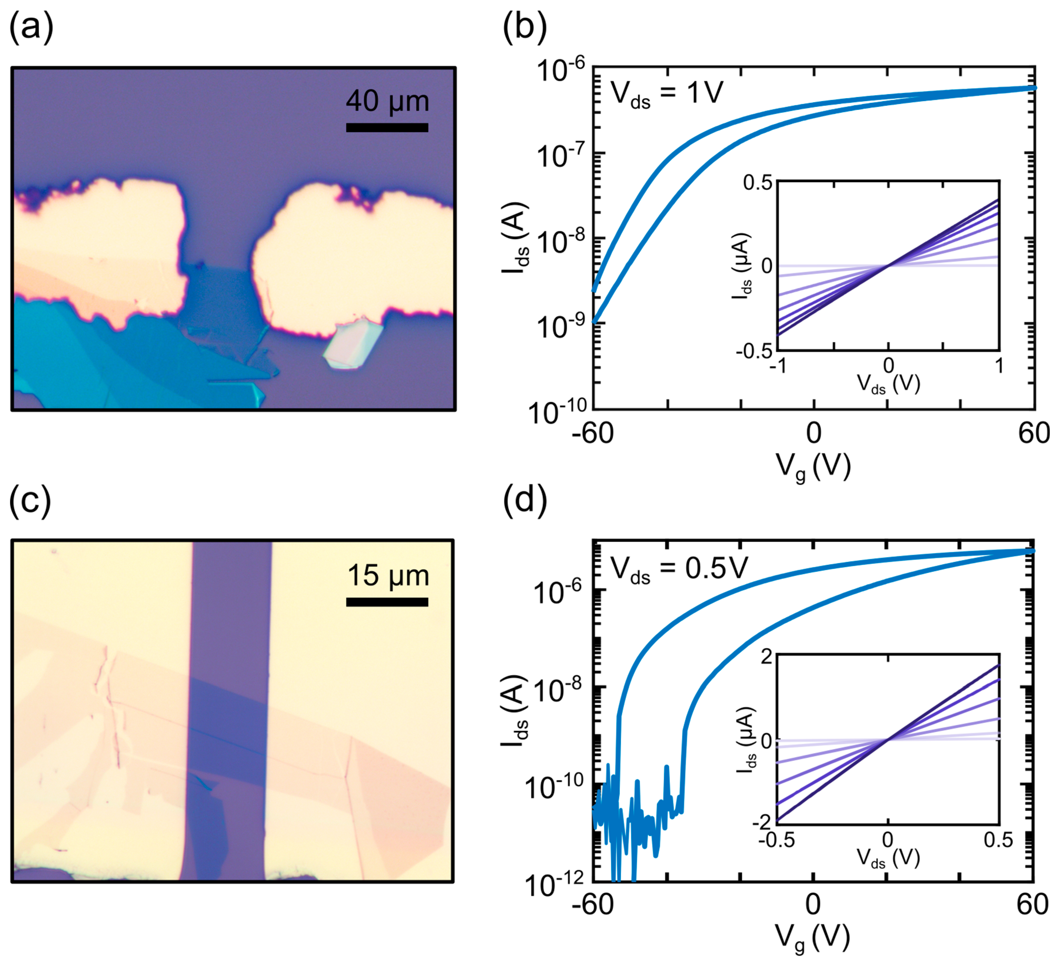
In order to illustrate the potential of these techniques to fabricate devices, we have deposited single-layer MoS2 flakes bridging the electrodes fabricated by metal deposition through the shadow masks. We employed a viscoelastic dry-transfer method based on Gel-Film stamps [18] to transfer a single-layer MoS2 flake to bridge the drain and source electrodes [19,20]. Figure 3a,c show optical microscopy images of devices fabricated with electrodes deposited through laser-ablated and vinyl + fiber shadow masks, respectively. After flake deposition, we perform a vacuum annealing step (2 h, 200 °C, 10−3 mbar) to improve the metal-semiconductor contact. We tested the electronic properties of the devices in a homebuilt probe station. Figure 3b,d show the source-drain current as a function of the back-gate voltage measured on the devices shown in Figure 3a,c. The transfer curves were measured under a constant source-drain bias VDS of 1 V with a gate voltage step speed of 1 Vs−1 (sweeping from −60 V to +60 V).
From these measurements, one can extract the field-effect mobility (μFE) of the fabricated field-effect transistors by following this expression [21]:
where IDS, VDS, and VGS are the source-drain current, source-drain voltage, and gate voltage, CG is the capacitance of the silicon oxide dielectric, and L and W are the length and width of the transistor channel. The devices shown in Figure 3 presented a mobility of 0.94 cm2 V−1 s−1 (laser-ablation mask) and 10.7 cm2 V−1 s−1 (vinyl + fiber mask). In Figure S3 in the Supporting Information, the reader will find the results of another two devices showing mobilities of 1 cm2 V−1 s−1 (for the laser-ablation mask) and 0.39 cm2 V−1 s−1 (for the vinyl + fiber mask). These field-effect measurements have been carried out in a three-terminal configuration without discounting for the effect of the contact resistance, and thus, the mobility values obtained here should be considered lower-bound estimates, as discounting for the contact resistance would lead to larger mobilities. It is interesting to note that we found that devices fabricated with electrodes fabricated by deposition through commercially available shadow masks (Ossila E321) lead to devices with similar characteristics in terms of threshold voltage, mobility, and current ON/OFF values achieved by our group [22,23] as well as others [24,25,26,27], with typical mobility values below 10 cm2 V−1 s−1 when using SiO2 as the dielectric material. Overcoming these values and getting closer to MoS2′s theoretical limit of around 200 cm2 V−1 s−1 would mean a change to a dielectric material with a higher dielectric constant [21,22,28]. Similarly, other transistor architectures can be designed, such as simple complete bottom gate tunnel field-effect transistors [29,30] or anywhere where pre-patterned electrodes are applicable with consideration of the achievable feature sizes.
3.3. Examples of Shadow Masks with More Complex Patterns
Figure 4 shows a few examples of other shadow mask designs fabricated with the laser ablation method on 40 µm thick aluminum foil to illustrate the flexibility of this technique in the rapid prototyping of devices. These patterns are chosen due to their usefulness when studying nanomaterial-based devices: a Hall bar, a four-terminal mask, and a mask designed to test in-plane electrical anisotropy.
4. Discussion and Conclusions
We have presented two different approaches for fabricating shadow masks for the evaporation of electrodes onto nanomaterials using a commercially available fiber laser engraving system or a vinyl cutting machine. The laser engraving of aluminum foil is able to produce shadow masks with line widths of 50 µm and minimum feature separation of 20 µm, although with a noticeable edge roughness and with complete flexibility over the pattern design. In the second technique, we use a vinyl cutter to define the pads and electrode leads, but we place a glass fiber to create a well-defined narrow separation between the drain and source electrodes. This technique allows us to create line widths of 200 µm separated by 15 µm (dependent on the glass fiber diameter) with a very sharp and well-defined electrode separation. Nonetheless, the vinyl + fiber technique is less flexible than the laser engraving one in terms of prototyping. We have proven the potential of these techniques by fabricating devices based on MoS2. A set of different patterns shows the ability to extend this technique to various applications in the field of microelectronics without limitation of substrate type and the freedom of post-material assembly due to pre-patterned structures. By using this method, patterns on flexible substrates can enable measurements in the field of strain engineering or biomedical applications. Our approaches are cost-effective and easily accessible methods for fabricating shadow masks with high resolution and accuracy, making them accessible to a wider range of laboratories. This work contributes a valuable addition to the field of nanoelectronics by providing simple and inexpensive methods for fabricating high-resolution shadow masks.
Supplementary Materials
The following supporting information can be downloaded at https://www.mdpi.com/article/10.3390/nanomanufacturing3030022/s1. Figure S1: Mask fabrication on standard kitchen aluminum foil; Figure S2: Atomic force characterization of the electrodes fabricated with different techniques; Figure S3: More examples of nanomaterial-based devices based on the electrodes fabricated with the homemade shadow masks; Video S1: Shadow mask laser writing process.
Author Contributions
Conceptualization, A.C.-G. and T.P.; methodology, T.P. and P.B.; software, T.P.; validation, T.P. and A.C.-G.; formal analysis, T.P. and P.B.; data curation, T.P., P.B. and E.S.V.; writing—original draft preparation, A.C.-G.; writing—review and editing, A.C.-G. and T.P.; visualization, T.P., A.C.-G. and E.S.V.; supervision, A.C.-G. All authors have read and agreed to the published version of the manuscript.
Funding
This research was funded by the European Research Council (ERC) through the project grant agreement n° 755655; the Ministry of Science and Innovation (Spain) through the projects PID2020-115566RB-I00 and TED2021-132267B-I00; the Horizon 2020 FLAG-ERA through the project To2Dox (JTC-2019-009); and Comunidad de Madrid through the project CAIRO-CM (Y2020/NMT-6661).
Data Availability Statement
The data of this study are available from the corresponding author upon reasonable request.
Acknowledgments
We thank Gulsum Ersu for her valuable help during the video shoot for the supporting information. This work was funded by the European Research Council (ERC) under the European Union’s Horizon 2020 research and innovation program (grant agreement n° 755655, ERC-StG 2017 project 2D-TOPSENSE) and the Ministry of Science and Innovation (Spain) through the projects PID2020-115566RB-I00 and TED2021-132267B-I00. We also acknowledge funding from the EU FLAG-ERA project To2Dox (JTC-2019-009) and the Comunidad de Madrid through the CAIRO-CM project (Y2020/NMT-6661). ChatGPT (GPT-3.5, OpenAI’s large-scale language-generation model) was used to improve the English grammar and writing style of this manuscript. The authors have reviewed, edited, and revised the ChatGPT-generated texts to their own liking and take ultimate responsibility for the content of this publication [31].
Conflicts of Interest
The authors declare no conflict of interest.
References
- Pugachev, M.V.; Duleba, A.I.; Galiullin, A.A.; Kuntsevich, A.Y. Micromask Lithography for Cheap and Fast 2D Materials Microstructures Fabrication. Micromachines 2021, 12, 850. [Google Scholar] [CrossRef] [PubMed]
- Khan, M.S.; Lachmayer, R.; Roth, B. Maskless Lithography for Versatile and Low Cost Fabrication of Polymer Based Micro Optical Structures. OSA Contin. 2020, 3, 2808. [Google Scholar] [CrossRef]
- Zhou, Y.X.; Johnson, A.T.; Hone, J.; Smith, W.F. Simple Fabrication of Molecular Circuits by Shadow Mask Evaporation. Nano Lett. 2003, 3, 1371–1374. [Google Scholar] [CrossRef]
- Tien, D.H.; Park, J.-Y.; Kim, K.B.; Lee, N.; Seo, Y. Characterization of Graphene-Based FET Fabricated Using a Shadow Mask. Sci. Rep. 2016, 6, 25050. [Google Scholar] [CrossRef]
- Bao, W.; Liu, G.; Zhao, Z.; Zhang, H.; Yan, D.; Deshpande, A.; LeRoy, B.; Lau, C.N. Lithography-Free Fabrication of High Quality Substrate-Supported and Freestanding Graphene Devices. Nano Res. 2010, 3, 98–102. [Google Scholar] [CrossRef]
- Yun, H.; Kim, S.; Kim, H.; Lee, J.; McAllister, K.; Kim, J.; Pyo, S.; Sung Kim, J.; Campbell, E.E.B.; Hyoung Lee, W.; et al. Stencil Nano Lithography Based on a Nanoscale Polymer Shadow Mask: Towards Organic Nanoelectronics. Sci. Rep. 2015, 5, 10220. [Google Scholar] [CrossRef]
- Liang, J.; Xu, K.; Toncini, B.; Bersch, B.; Jariwala, B.; Lin, Y.; Robinson, J.; Fullerton-Shirey, S.K. Impact of Post-Lithography Polymer Residue on the Electrical Characteristics of MoS2 and WSe2 Field Effect Transistors. Adv. Mater. Interfaces 2019, 6, 1801321. [Google Scholar] [CrossRef]
- Shen, X.; Wang, H.; Yu, T. How Do the Electron Beam Writing and Metal Deposition Affect the Properties of Graphene during Device Fabrication? Nanoscale 2013, 5, 3352. [Google Scholar] [CrossRef]
- Katagiri, Y.; Nakamura, T.; Ishii, A.; Ohata, C.; Hasegawa, M.; Katsumoto, S.; Cusati, T.; Fortunelli, A.; Iannaccone, G.; Fiori, G.; et al. Gate-Tunable Atomically Thin Lateral MoS2 Schottky Junction Patterned by Electron Beam. Nano Lett. 2016, 16, 3788–3794. [Google Scholar] [CrossRef]
- Cao, Y.; Mishchenko, A.; Yu, G.L.; Khestanova, E.; Rooney, A.P.; Prestat, E.; Kretinin, A.V.; Blake, P.; Shalom, M.B.; Woods, C.; et al. Quality Heterostructures from Two-Dimensional Crystals Unstable in Air by Their Assembly in Inert Atmosphere. Nano Lett. 2015, 15, 4914–4921. [Google Scholar] [CrossRef]
- Castellanos-Gomez, A.; Vicarelli, L.; Prada, E.; Island, J.O.; Narasimha-Acharya, K.L.; Blanter, S.I.; Groenendijk, D.J.; Buscema, M.; Steele, G.A.; Alvarez, J.V.; et al. Isolation and Characterization of Few-Layer Black Phosphorus. 2D Mater. 2014, 1, 025001. [Google Scholar] [CrossRef]
- Aljada, M.; Mutkins, K.; Vamvounis, G.; Burn, P.; Meredith, P. High Quality Shadow Masks for Top Contact Organic Field Effect Transistors Using Deep Reactive Ion Etching. J. Micromech. Microeng. 2010, 20, 075037. [Google Scholar] [CrossRef]
- Zhang, H.; Guo, X.; Niu, W.; Xu, H.; Wu, Q.; Liao, F.; Chen, J.; Tang, H.; Liu, H.; Xu, Z.; et al. Multilayer Si Shadow Mask Processing of Wafer-Scale MoS2 Devices. 2D Mater. 2020, 7, 025019. [Google Scholar] [CrossRef]
- Tomczyk, M.; Kubik, P.; Waliszewski, W. Optimization of the Ablative Laser Cutting of Shadow Mask for Organic FET Electrode Fabrication. Electronics 2020, 9, 2184. [Google Scholar] [CrossRef]
- Elhami Nik, F.; Matthiesen, I.; Herland, A.; Winkler, T. Low-Cost PVD Shadow Masks with Submillimeter Resolution from Laser-Cut Paper. Micromachines 2020, 11, 676. [Google Scholar] [CrossRef] [PubMed]
- Staley, N.; Wang, H.; Puls, C.; Forster, J.; Jackson, T.N.; McCarthy, K.; Clouser, B.; Liu, Y. Lithography-Free Fabrication of Graphene Devices. Appl. Phys. Lett. 2007, 90, 143518. [Google Scholar] [CrossRef]
- Castellanos-Gomez, A.; Smit, R.H.M.; Agraït, N.; Rubio-Bollinger, G. Spatially Resolved Electronic Inhomogeneities of Graphene Due to Subsurface Charges. Carbon 2012, 50, 932–938. [Google Scholar] [CrossRef]
- Castellanos-Gomez, A.; Buscema, M.; Molenaar, R.; Singh, V.; Janssen, L.; van der Zant, H.S.J.; Steele, G.A. Deterministic Transfer of Two-Dimensional Materials by All-Dry Viscoelastic Stamping. 2d Mater. 2014, 1, 011002. [Google Scholar] [CrossRef]
- Yang, R.; Zheng, X.; Wang, Z.; Miller, C.J.; Feng, P.X.-L. Multilayer MoS2 Transistors Enabled by a Facile Dry-Transfer Technique and Thermal Annealing. J. Vac. Sci. Technol. B Nanotechnol. Microelectron. Mater. Process. Meas. Phenom. 2014, 32, 61203. [Google Scholar]
- Frisenda, R.; Navarro-Moratalla, E.; Gant, P.; De Lara, D.P.; Jarillo-Herrero, P.; Gorbachev, R.V.; Castellanos-Gomez, A. Recent Progress in the Assembly of Nanodevices and van Der Waals Heterostructures by Deterministic Placement of 2D Materials. Chem. Soc. Rev. 2018, 47, 53–68. [Google Scholar] [CrossRef]
- Radisavljevic, B.; Radenovic, A.; Brivio, J.; Giacometti, V.; Kis, A. Single-Layer MoS2 Transistors. Nat. Nanotechnol. 2011, 6, 147–150. [Google Scholar] [CrossRef]
- Puebla, S.; Pucher, T.; Rouco, V.; Sanchez-Santolino, G.; Xie, Y.; Zamora, V.; Cuellar, F.A.; Mompean, F.J.; Leon, C.; Island, J.O.; et al. Combining Freestanding Ferroelectric Perovskite Oxides with Two-Dimensional Semiconductors for High Performance Transistors. Nano Lett. 2022, 22, 7457–7466. [Google Scholar] [CrossRef] [PubMed]
- Xie, Y.; Çakıroğlu, O.; Hu, W.; He, K.; Puebla, S.; Pucher, T.; Zhao, Q.; Ma, X.; Munuera, C.; Castellanos-Gomez, A. Laser Trimming for Lithography-Free Fabrications of MoS2 Devices. Nano Res. 2023, 16, 5042–5046. [Google Scholar] [CrossRef]
- Qiu, H.; Pan, L.; Yao, Z.; Li, J.; Shi, Y.; Wang, X. Electrical Characterization of Back-Gated Bi-Layer MoS2 Field-Effect Transistors and the Effect of Ambient on Their Performances. Appl. Phys. Lett. 2012, 100, 123104. [Google Scholar] [CrossRef]
- Late, D.J.; Liu, B.; Matte, H.S.S.R.; Dravid, V.P.; Rao, C.N.R. Hysteresis in Single-Layer MoS2 Field Effect Transistors. ACS Nano 2012, 6, 5635–5641. [Google Scholar] [CrossRef] [PubMed]
- Ghatak, S.; Pal, A.N.; Ghosh, A. Nature of Electronic States in Atomically Thin MoS2 Field-Effect Transistors. ACS Nano 2011, 5, 7707–7712. [Google Scholar] [CrossRef]
- Li, T.; Du, G.; Zhang, B.; Zeng, Z. Scaling Behavior of Hysteresis in Multilayer MoS2 Field Effect Transistors. Appl. Phys. Lett. 2014, 105, 093107. [Google Scholar] [CrossRef]
- Yoon, Y.; Ganapathi, K.; Salahuddin, S. How Good Can Monolayer MoS2 Transistors Be? Nano Lett. 2011, 11, 3768–3773. [Google Scholar] [CrossRef]
- Nourbakhsh, A.; Zubair, A.; Dresselhaus, M.S.; Palacios, T. Transport Properties of a MoS2/WSe2 Heterojunction Transistor and Its Potential for Application. Nano Lett. 2016, 16, 1359–1366. [Google Scholar] [CrossRef]
- Balaji, Y.; Smets, Q.; Śzabo, Á.; Mascaro, M.; Lin, D.; Asselberghs, I.; Radu, I.; Luisier, M.; Groeseneken, G. MoS2/MoTe2 Heterostructure Tunnel FETs Using Gated Schottky Contacts. Adv. Funct. Mater. 2020, 30, 1905970. [Google Scholar] [CrossRef]
- Castellanos-Gomez, A. Good Practices for Scientific Article Writing with ChatGPT and Other Artificial Intelligence Language Models. Nanomanufacturing 2023, 3, 135–138. [Google Scholar] [CrossRef]
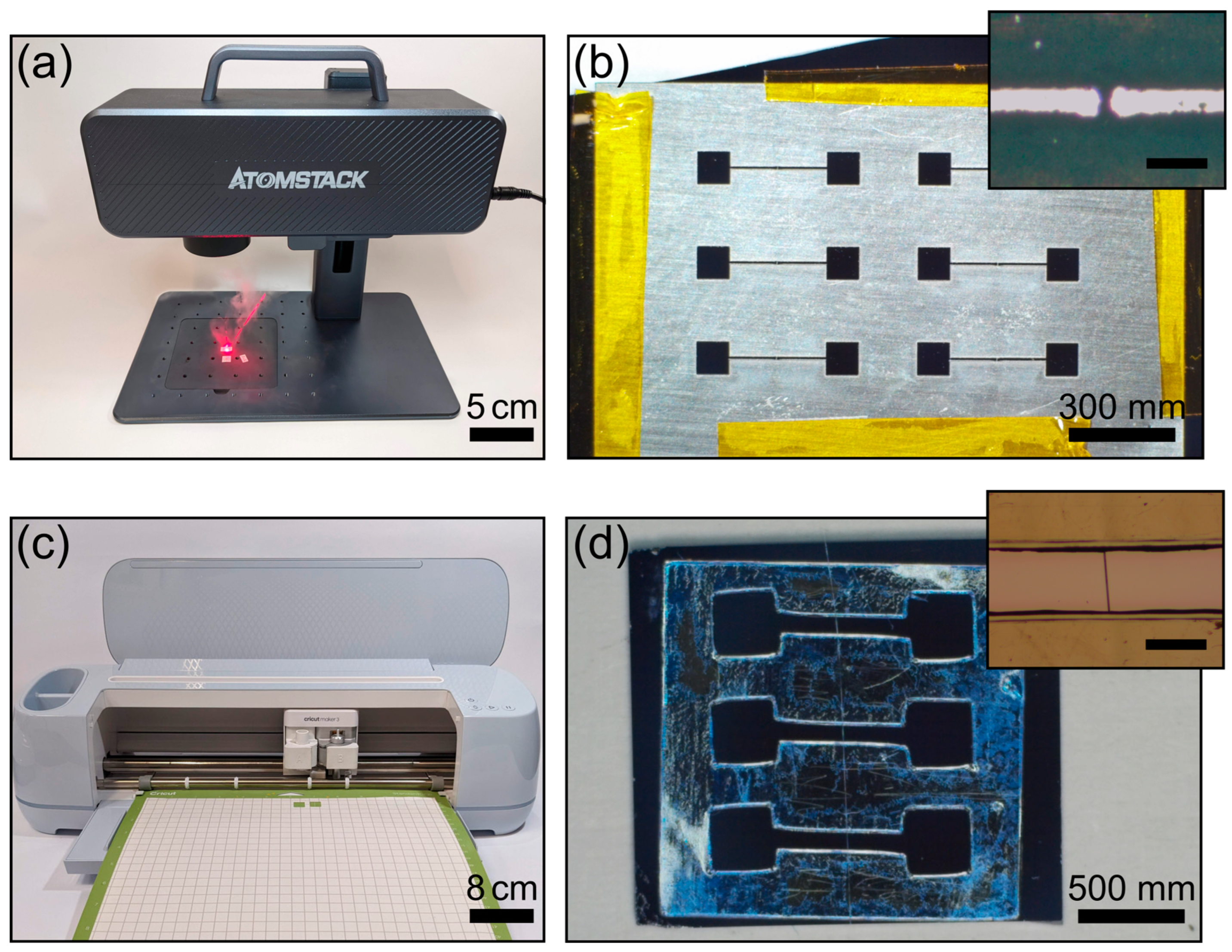
Figure 1.
Fabrication of shadow masks with commercially available laser engraver and vinyl cutter systems. (a) Picture of a fiber laser engraving system Atomstack M4 while cutting thick aluminum foil. (b) Picture of one of the fabricated shadow masks with drain and source electrodes separated by different distances ranging from 20 µm to 40 µm, fixed on a SiO2/Si substrate with Kapton tape. (Inset) Optical microscopy image of the separation between the drain and source electrode at the central part of the ‘bar-shaped’ lead. The scale bar is 100 µm. (c) Picture of a Cricut Maker 3 vinyl cutter system used to prepare a vinyl stencil mask with the pads and the electrode leads. (d) Vinyl mask adhered onto a SiO2/Si substrate using the adhesive of the vinyl. A 15 µm diameter glass fiber was deposited onto the surface prior to adhering the mask to define the separation between drain and source electrodes (see inset, scale bar: 500 µm).

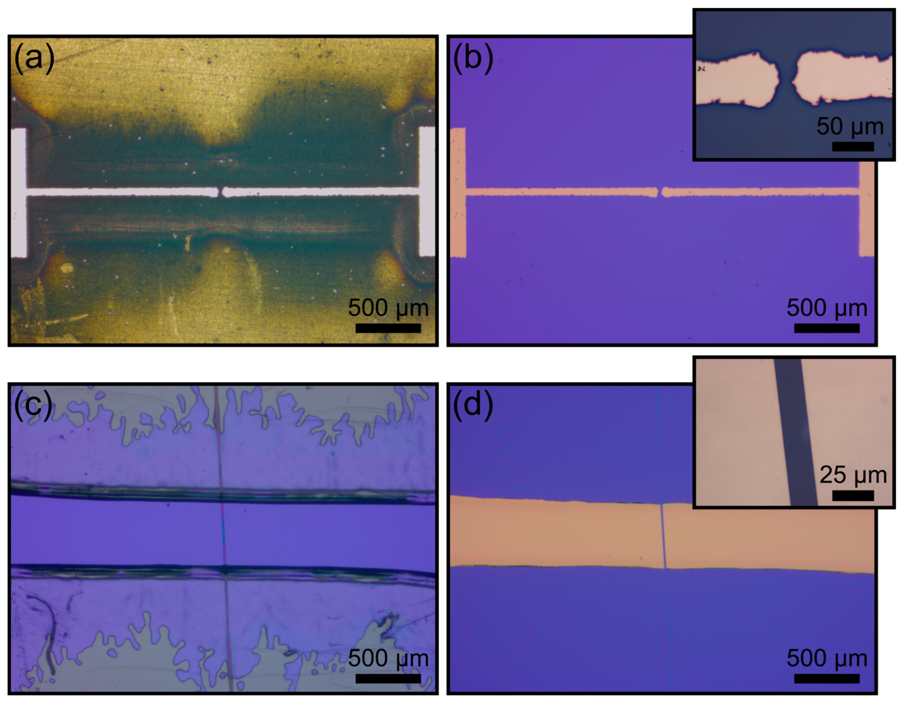
Figure 2.
Resulting electrodes after evaporation through the homebuilt shadow masks. (a) Optical microscopy image of a drain-source mask patterned on thick aluminum foil with the fiber laser engraver system. (b) Optical microscopy image of the resulting electrodes after evaporating Au (45 nm)/Ti (5 nm) onto a SiO2/Si substrate. (Inset) Higher magnification image of the gap between drain and source electrodes. (c) Optical microscopy image of a drain-source mask fabricated by combining the vinyl mask with a 15 µm diameter glass fiber adhered onto a SiO2/Si before metal deposition. (d) Optical microscopy image of the resulting electrodes after evaporating Au (45 nm)/Ti (5 nm) onto a SiO2/Si substrate. (Inset) Higher magnification image of the gap between drain and source electrodes.

Figure 3.
Example of nanomaterial-based devices based on the electrodes fabricated with the homemade shadow masks. (a) Optical microscopy image of a single-layer MoS2 flake bridging the drain and source electrodes fabricated with the laser-ablated shadow mask. (b) Semi-logarithmic transfer curve of the resulting MoS2 field-effect transistor for a constant bias VDS of 1 V. (Inset) Gate-dependent IVs for gate voltages of −60 to 60 V. (c) Optical microscopy image of a transferred single-layer MoS2 flake bridging the drain and source electrodes fabricated with vinyl + glass fiber mask. (d) Semi-logarithmic transfer curve of the resulting MoS2 field-effect transistor for a constant bias VDS of 0.5 V. (Inset) Gate-dependent IVs for gate voltages of −60 to 60 V.

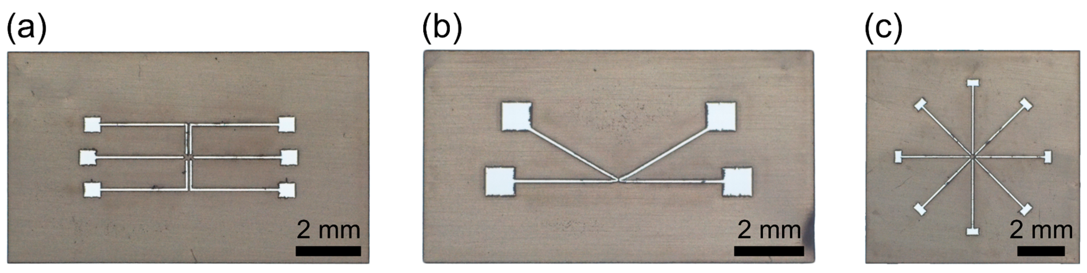
Figure 4.
Examples of different shadow mask patterns created with the fiber laser engraving system. (a) Hall bar. (b) Four-terminal configuration. (c) Electrode probes to test in-plane anisotropic materials.
Figure 4.
Examples of different shadow mask patterns created with the fiber laser engraving system. (a) Hall bar. (b) Four-terminal configuration. (c) Electrode probes to test in-plane anisotropic materials.

Disclaimer/Publisher’s Note: The statements, opinions and data contained in all publications are solely those of the individual author(s) and contributor(s) and not of MDPI and/or the editor(s). MDPI and/or the editor(s) disclaim responsibility for any injury to people or property resulting from any ideas, methods, instructions or products referred to in the content. |
© 2023 by the authors. Licensee MDPI, Basel, Switzerland. This article is an open access article distributed under the terms and conditions of the Creative Commons Attribution (CC BY) license (https://creativecommons.org/licenses/by/4.0/).
Share and Cite
MDPI and ACS Style
Pucher, T.; Bastante, P.; Sánchez Viso, E.; Castellanos-Gomez, A. Low-Cost Shadow Mask Fabrication for Nanoelectronics. Nanomanufacturing 2023, 3, 347-355. https://doi.org/10.3390/nanomanufacturing3030022
AMA Style
Pucher T, Bastante P, Sánchez Viso E, Castellanos-Gomez A. Low-Cost Shadow Mask Fabrication for Nanoelectronics. Nanomanufacturing. 2023; 3(3):347-355. https://doi.org/10.3390/nanomanufacturing3030022
Chicago/Turabian StylePucher, Thomas, Pablo Bastante, Estrella Sánchez Viso, and Andres Castellanos-Gomez. 2023. "Low-Cost Shadow Mask Fabrication for Nanoelectronics" Nanomanufacturing 3, no. 3: 347-355. https://doi.org/10.3390/nanomanufacturing3030022