Design of Control Circuit for Tunable Semiconductor Laser for Fiber Sensing


College of Ocean Science and Engineering, Shandong University of Science and Technology, Qingdao 266590, China
*
Author to whom correspondence should be addressed.
Hardware 2023, 1(1), 4-28; https://doi.org/10.3390/hardware1010003
Submission received: 28 October 2023
/
Revised: 15 November 2023
/
Accepted: 22 November 2023
/
Published: 24 November 2023
Abstract
:Semiconductor lasers have garnered significant prominence in diverse domains, including fiber optic communication and precision measurement, owing to their remarkable attributes such as compact size, lightweight construction, broad wavelength range, and tunability. Among these lasers, tunable semiconductor lasers assume a pivotal role in fiber Bragg grating demodulation systems, as the stability of their output wavelength and power directly influences the overall performance of the demodulation system. Ensuring the steadfastness of the output power and emission wavelength necessitates the provision of a stable driving current and the maintenance of a consistent operating temperature. Consequently, a specialized driver circuit necessitates meticulous design and implementation. In this investigation, a novel STM32 microcontroller-based tunable laser control circuit was meticulously developed to meet the practical requisites of fiber Bragg grating sensor demodulation. Leveraging the advanced capabilities of the MAX5113 current control chip and the MAX1978 temperature control chip, a dedicated circuit for constant current driving and temperature regulation of the tunable semiconductor laser was meticulously devised. Additionally, the design incorporates cutting-edge components, including a photodetector and an ADC conversion module, to seamlessly fulfill the intricate demands of the fiber Bragg grating demodulation system. The conclusive experimental results conclusively demonstrate the excellent stability of the output current produced by the constant current driving circuit, the minimal fluctuations observed in laser temperature, and the remarkable tunability of the laser’s output wavelength within the precise range of 1525 to 1550 nm. Notably, the wavelength fluctuations are confined to an impressively narrow margin of just 3 pm, providing definitive evidence that the design fully satisfies the practical requirements.
1. Introduction
Fiber optic sensing technology, as a miniaturized optical device, is a byproduct of the advancement in fiber optic communication technology and represents a novel sensing technique. The operating principle of fiber optic sensing lies in the modulation of intrinsic parameters of light by external environmental factors, which influence the propagation characteristics of light waves as they traverse through optical fibers. In other words, fiber optic sensing harnesses the impact of external environmental factors, such as temperature, deformation, and vibration, to modulate the characteristic parameters of light waves propagating through optical fibers, enabling the extraction of valuable information regarding various physical quantities present in the surrounding environment [1]. Fiber optic sensing technology has gained widespread application in the field of engineering [2,3,4], attracting the attention of experts and scholars worldwide [5,6,7]. In the wide range of applications involving fiber optic gratings, the optical signal acts as a medium for carrying the measured physical quantity. To demodulate such signals effectively, a tunable laser with a broad tuning range, excellent stability, and precise linewidth is essential in the demodulation system [8]. Tunable lasers serve as a crucial component in a wide range of applications, including spectral analysis, wavelength division multiplexing, and grating demodulation, playing an essential role in each of these areas [9].
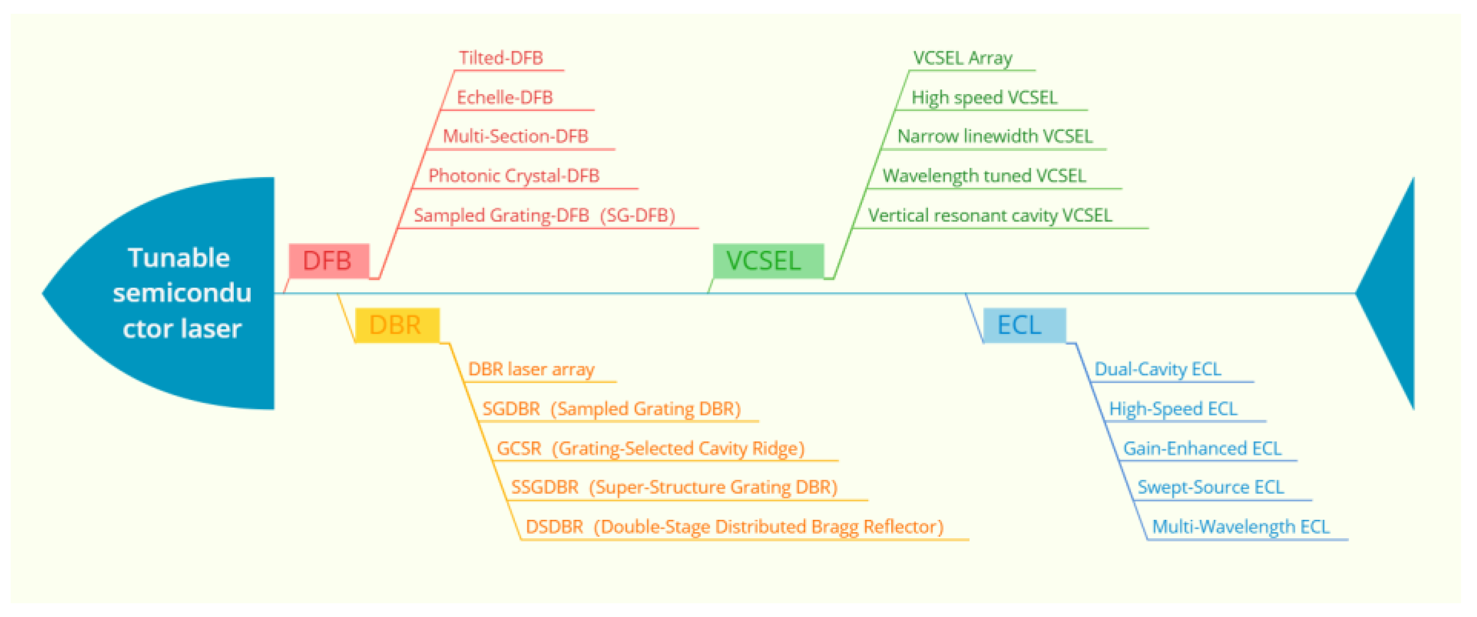
Based on the structural characteristics of semiconductor lasers, they can be broadly categorized into four main types: distributed feedback semiconductor lasers (DFBs), external cavity semiconductor lasers (ECLs), distributed Bragg reflector semiconductor lasers (DBRs), and vertical-cavity surface-emitting lasers (VCSELs). These classifications are based on distinct design principles and offer suitable laser options for various applications in academic and scientific domains [10,11,12]. Figure 1 presents the classification diagram illustrating the evolutionary development of tunable semiconductor lasers.
The importance of the driver control circuit for tunable semiconductor lasers in fiber optic sensing demodulation systems cannot be overstated. It serves as a crucial component, offering a highly accurate and stable light source for the precise demodulation of fiber optic sensing signals [13]. The laser control circuit plays a crucial role in precisely controlling the wavelength of the laser, ensuring the alignment of the fiber optic grating’s characteristics with the light source. This alignment significantly improves the accuracy and reliability of the demodulation system [14,15]. Over time, the development of the laser control circuit has witnessed the emergence of various techniques and approaches, further enhancing its effectiveness. In the course of its development, a wide range of techniques and methods have emerged. Tunable semiconductor lasers employ temperature, current, and mechanical adjustments to achieve wavelength tuning. Among these methods, the current control approach involves modulating the injection current of the semiconductor laser to alter the output wavelength. This technique provides a broad tuning bandwidth and rapid tuning speed, albeit potentially leading to reduced output optical power [16]. On the other hand, the temperature control method adjusts the temperature within the semiconductor laser cavity to modify the refractive index of the active region, enabling wavelength tuning. However, this method exhibits a slower tuning speed and narrower tunable bandwidth, typically in the range of a few nanometers [17,18]. In general, current tuning is well-suited for applications that necessitate rapid tuning and a broad wavelength range, whereas temperature tuning is ideal for applications that prioritize high precision and stability. Depending on the specific requirements of the application, one can select the appropriate tuning method or even combine both approaches to achieve enhanced wavelength tuning performance.
In the realm of driver circuit research for tunable semiconductor lasers, several challenges persist and require attention. These challenges encompass the enhancement of tuning speed, expansion of the tuning range, and improvement of stability. Addressing these challenges is essential for advancing the field of tunable semiconductor lasers and enabling their broader applicability in various scientific and technological domains. The primary objective of this article is to present an optimized light source for wavelength demodulation systems utilizing current-tunable semiconductor lasers. By precisely controlling the current and ensuring temperature stability, the semiconductor laser can achieve long-term operational stability [19,20]. Through a comprehensive examination of the characteristics and performance of current-tunable semiconductor lasers, this study highlights their inherent advantages and suitability as light sources for fiber sensing demodulation. Ultimately, the research provides valuable insights for the design and implementation of driver control circuits tailored to current-tunable semiconductor lasers, effectively meeting the stringent requirements of fiber sensing demodulation systems.
The remaining research is organized as follows: Section 2 provides an introduction to the working principles of tunable semiconductor lasers, Section 3 presents an overview of the overall control design of the light source in tunable semiconductor lasers, Section 4 analyzes the results obtained in the study, Section 5 discusses the research methodology and results presented in the paper, Section 6 provides a summary and conclusion of the paper.
2. The Working Principle of Tunable Semiconductor Lasers
Driven by the ongoing advancements in fiber optic communication technology and wavelength division multiplexing (WDM), the field of tunable semiconductor lasers has witnessed the integration of diverse tuning structures, enabling the attainment of broader and more continuous laser output. The rapid advancements and widespread adoption of cutting-edge tunable semiconductor devices have significantly improved performance and stability. The continuous developments and applications in the field of fiber sensing have established a solid foundation for the advancement of fiber sensing demodulation technology, thereby offering a novel and superior solution [17].
The Super-Structure Grating Distributed Bragg Reflector (SSG-DBR) represents a distinctive configuration employed in tunable semiconductor laser structures [4,21]. The super-structure grating constitutes a refractive index distribution structure featuring periodic variations, typically comprising multiple layers of dielectric materials with periodic variations. This design enables the modulation of light’s wavelength and propagation direction. On the other hand, the Distributed Bragg Reflector (DBR) functions as an optical reflector, establishing an optical reflection structure through periodic alterations of the refractive index within a semiconductor material. This arrangement selectively reflects light of specific wavelengths, serving a crucial role in the overall operation of the SSG-DBR tunable semiconductor laser. The SSG-DBR laser combines the characteristics of both the super-structure grating and the distributed Bragg reflector, allowing for wavelength tuning of the laser output by adjusting the period of the super-structure grating and the refractive index distribution of the distributed Bragg reflector. By controlling parameters such as injected current or temperature, the refractive index of the super-structure grating and distributed Bragg reflector can be modulated, enabling flexible adjustment of the laser wavelength. Compared to traditional DBR lasers, the SSG-DBR laser offers advantages such as a larger wavelength tuning range, lower tuning voltage, higher resolution, and faster tuning response. These features make the SSG-DBR laser highly promising for a wide range of applications in optical communication, optical sensing, and spectroscopic analysis.
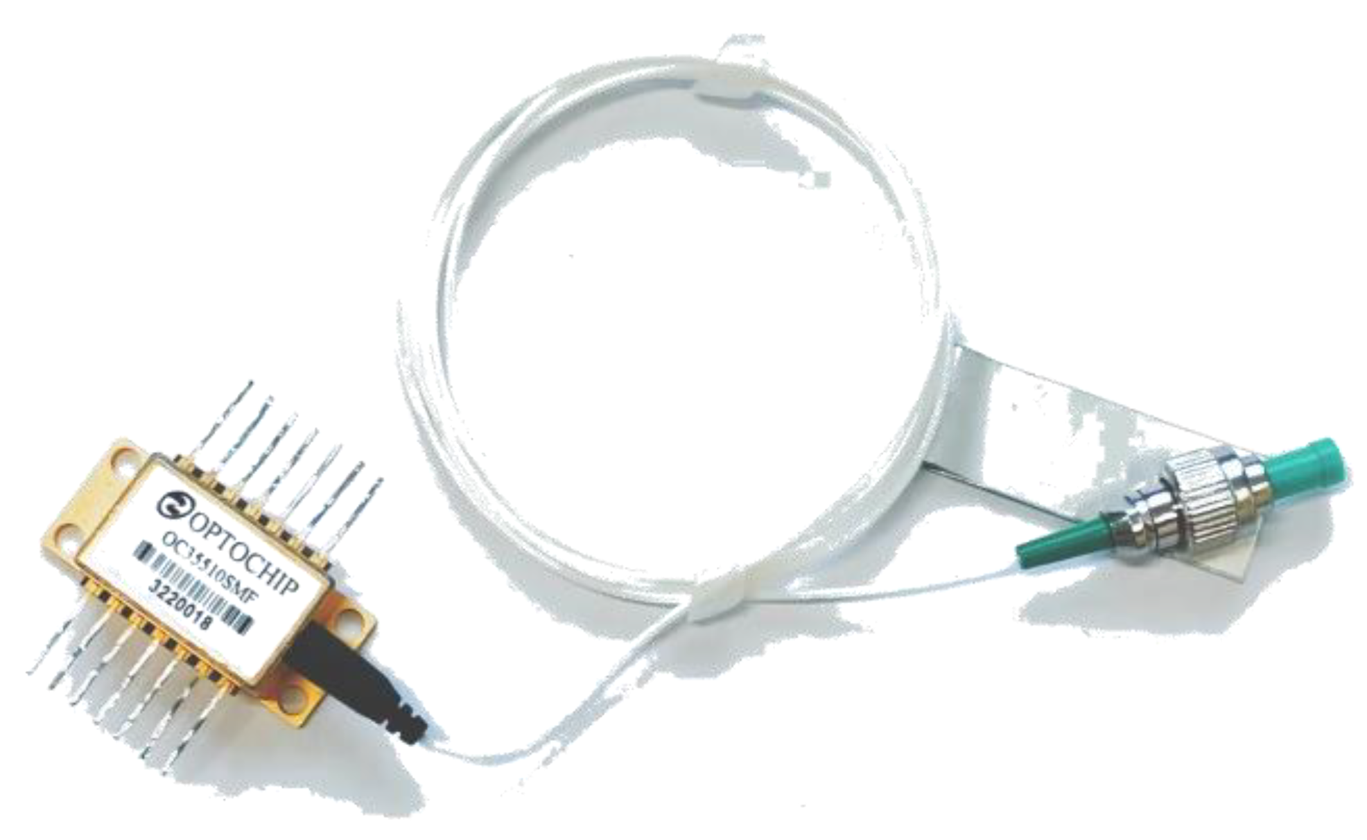
This study utilizes a 40 nm wideband tunable SSG-DBR laser chip developed by Shandong Zhongxin Optoelectronics Technology Co., Ltd. (Jinan, China). The chip is fabricated using InP/InGaAsP materials and achieves a wavelength tuning range of approximately 40 nm by incorporating two superstructure gratings, positioned at the front and back of the chip. The chip demonstrates several prominent characteristics, including high-output optical power, exceptional power stability, and rapid wavelength tuning speed. Through the manipulation of gratings and phase currents, the chip enables continuous wavelength tunability with a tuning speed in the nanosecond range. It exhibits remarkable capabilities for flexible and swift wavelength switching and ensures a stable laser output power by adjusting the current of the Semiconductor Optical Amplifier (SOA). This particular laser chip serves as a fundamental light source and finds extensive applications in various fiber optic grating sensing systems. Its utilization allows for real-time monitoring of physical parameters such as stress, temperature, displacement, vibration, and deformation. These applications have direct implications for structural safety warnings in the context of bridges, tunnels, and large-scale buildings. Moreover, the chip plays a crucial role in ensuring safety in wind power generation, power transmission systems, coal mining, and oil enterprises by facilitating their production and operational security. Furthermore, it contributes significantly to the safety monitoring of high-speed railways, expressways, and rail transportation systems. Figure 2 depicts the 40 nm tunable laser module.
The laser is a typical multi-electrode DBR-type tunable semiconductor laser, typically consisting of three components: the grating section, the phase section, and the active section [9]. The grating section, composed of a superstructure grating, facilitates wavelength-selective reflection. The phase section regulates the phase to control the laser’s output wavelength. The active section functions as the amplification region of the laser, responsible for optical amplification and stimulated emission. The synergistic operation of these three components enables the SSG-DBR laser to achieve wavelength tuning and maintain a stable laser output [22]. The multi-electrode tuning mechanism is a sophisticated wavelength tuning technique designed for tunable lasers. By precisely controlling the injection current of different electrodes, this mechanism enables both coarse and fine adjustments of the laser’s wavelength. Additionally, the optical gain and power can be fine-tuned by adjusting the current of the active region. The tuning process involves injecting various currents into the passive region, which alters the refractive index of the grating section and consequently achieves coarse wavelength adjustment. The grating section plays a pivotal role in controlling wavelength selection within the laser. Further refinement is achieved by adjusting the current input of the phase section, allowing for precise tuning of the refractive index [9,17] and, consequently, the laser’s wavelength within a narrower range. Simultaneously, controlling the active region’s current modifies the laser’s optical gain and power, a crucial capability for adjusting the intensity and power of the output light in specific applications. Through the synchronized tuning of both the grating and phase sections, the multi-electrode tuning mechanism delivers high-resolution wavelength tuning output. Lasers generally exhibit a wavelength range spanning several tens of nanometers, and with precise current regulation, they can achieve quasi-continuous wavelength output [23,24].
The laser used in this study consists of five parts: two grating sections, a phase section, a gain region, and a fiber amplification region. The grating sections serve as the pivotal components for adjusting the laser’s output wavelength. By altering the grating period, they effectively modify the operating wavelength of the laser. Through meticulous adjustment of these two grating sections, precise wavelength calibration can be attained, thus enabling coverage of various wavelengths within the C-band. Such a design affords the laser high precision and flexibility in wavelength tuning. It facilitates fine-tuning of the laser’s output wavelength by adjusting the relative phase difference between the two grating sections. Precise control of the phase section is essential for achieving highly accurate wavelength tuning. The gain region acts as the core of the laser, providing optical amplification and lasing. Through current injection and stimulated emission, high-gain optical signals are generated within this region. The characteristics of the gain region directly influence the laser’s output power and optical gain. Additionally, the fiber amplification region amplifies the optical signal and allows for independent control of the current input. This enables independent adjustment of the laser’s power output. The fiber amplification region also offers the capability of laser output switching, ensuring a stable laser wavelength output and preventing mode hopping. By controlling the current input to the fiber amplification region, the laser output can be effectively switched on or off. This capability allows for precise control over the laser’s operation, maintaining a consistent and stable wavelength output and preventing unwanted mode transitions or fluctuations [24]. Through the combination and precise control of these five components, the laser can achieve continuous tunable output within the wavelength range of 1525 to 1550 nm.
The laser’s pin configurations, as illustrated in Table 1, are pivotal for controlling the laser’s performance and functionality. Each pin serves a critical role in governing various aspects of the laser’s operation. By meticulously regulating the current input to each pin, precise control can be exerted over crucial parameters such as optical gain, optical power output, wavelength tuning, and power control. This meticulous control ensures the laser operates with stability and produces an output of exceptional quality.
3. Overall Design of Control Circuit for Tunable Semiconductor Laser Light Source
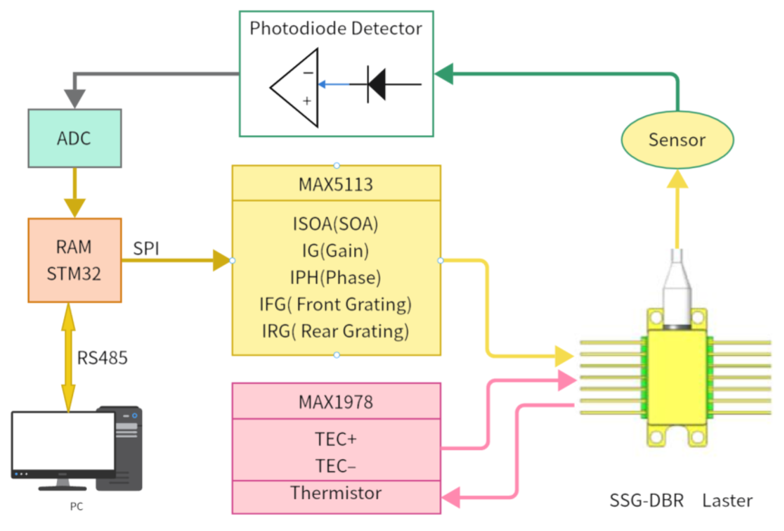
Figure 3 illustrates the block diagram of the control principle for a tunable laser light source. This block diagram serves as a foundation for controlling the tunable light source and can also be applied in optical fiber grating demodulation systems. To ensure a stable laser output and achieve continuous tunable light source output covering the C-band, specific components such as appropriate microcontrollers, high-precision constant current source controllers, high-precision temperature controllers, and ADC modules need to be carefully chosen based on the specifications of the 40 nm tunable semiconductor laser. The microcontroller’s application program plays a key role in coordinating the operation of each submodule. The constant current source controller regulates high-precision currents across five channels. The high-precision temperature controller continuously samples the temperature of the laser module and maintains it at a constant level [25].
3.1. Design of the Core Microcontroller
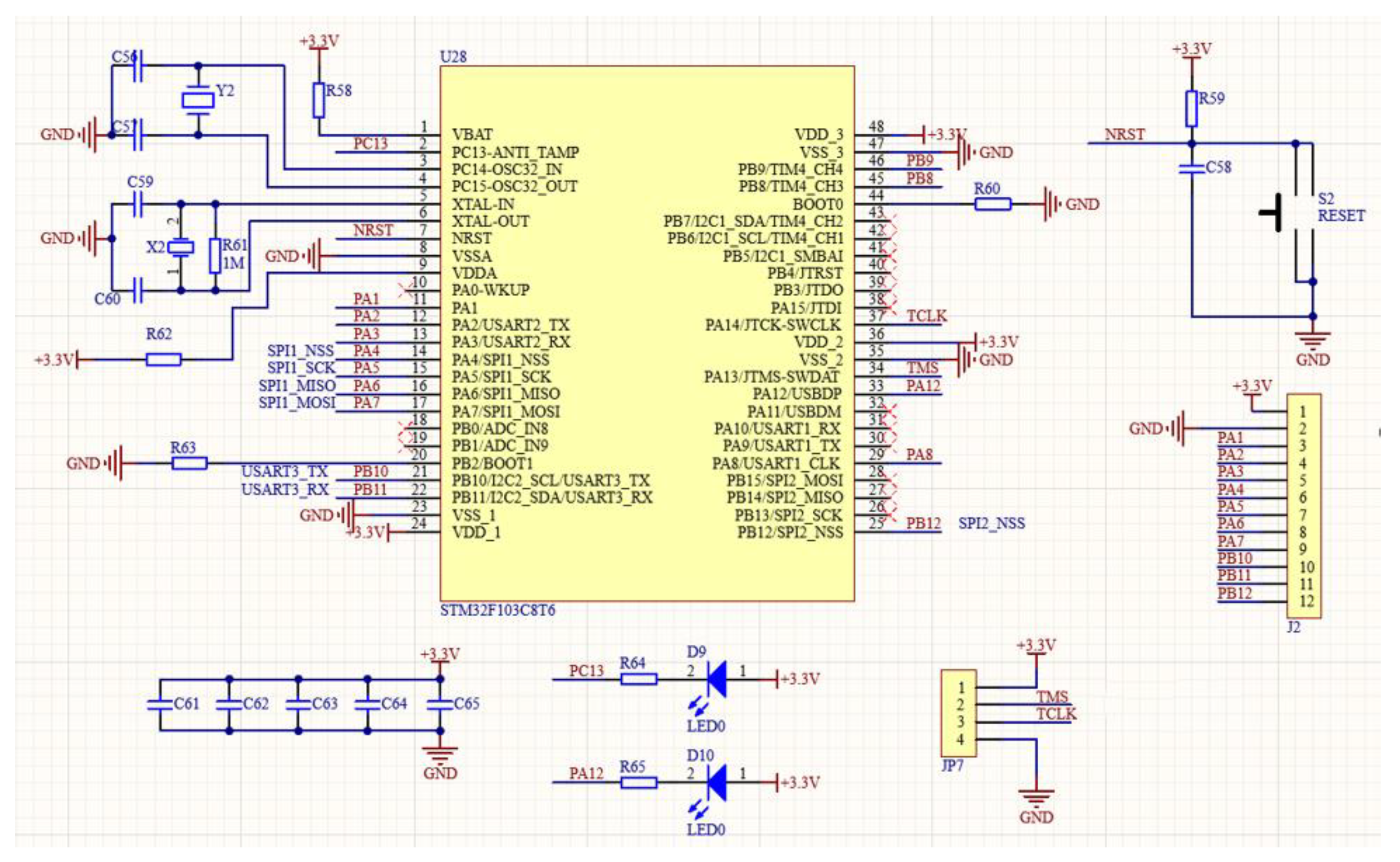
After conducting performance and requirements analyses on various modules, we have selected the STM32F103C8T6 chip as the core microcontroller. This chip boasts a 32-bit ARM Cortex-M3 core, which provides exceptional performance and low power consumption. Operating at a maximum frequency of 72 MHz, it delivers robust processing capabilities and real-time performance, making it an ideal choice for applications that demand high processing performance. The STM32F103C8T6 chip integrates 64 KB of flash memory for storing application code and data, while its 20 KB of static random-access memory (SRAM) ensures rapid data storage and access. Additionally, it offers a diverse range of peripheral interfaces, including multiple general-purpose input/output (GPIO) ports, serial communication interfaces such as USART, SPI, and I2C, timers, and an analog-to-digital converter (ADC). These interfaces facilitate seamless connectivity and control of external devices. One noteworthy advantage of the STM32F103C8T6 is its outstanding low-power characteristics, enabling prolonged operation in battery-powered or power-sensitive applications. It supports various power-saving modes that can be flexibly configured to achieve optimal power efficiency. The minimum system schematic is depicted in Figure 4.
The microprocessor assumes the key responsibility of coordinating and managing the operation of distinct sub-modules to ensure the holistic functionality of the system [26]. These sub-modules encompass the constant current control module, temperature control module, ADC conversion module, and RS485 serial communication module [20,27].
In the constant current driving circuit, the microcontroller employs the SPI bus to control the MAX5113 single-chip integrated constant current source chip. This configuration enables precise control of the laser, including the configuration of five input current channels and the output of stable and high-resolution wavelengths. The MAX5113 integrates a 9-channel, high-precision 14-bit current output digital-to-analog converter (DAC), delivering advantages such as high integration, simplified external circuit design, and enhanced reliability. Leveraging SPI communication, the microcontroller can transmit control commands and data to the MAX5113, facilitating current configuration and adjustment for each channel while enabling independent control of multiple lasers. While a traditional constant current source circuit comprising a digital-to-analog (DA) circuit, operational amplifiers, power MOSFETs, and current sensing resistors can also achieve five-channel current control for laser modulation, it is burdened with a complex circuit design, a large PCB footprint, and susceptibility to external interference. In contrast, utilizing a single-chip integrated constant current source IC like the MAX5113 offers notable advantages in terms of performance, integration, stability, and cost-effectiveness for laser wavelength tuning, surpassing the aforementioned conventional discrete constant current sources. By adopting the MAX5113 single-chip integrated constant current source, it becomes feasible to realize five-channel current combination control for laser modulation, resulting in improved performance, higher integration level, enhanced stability, and overall cost-effectiveness.
In the laser temperature control process, the MAX1978 is employed as the controller for the thermoelectric cooler (TEC). This chip offers a bipolar current drive output with a range of ±3 A. The design incorporates a butterfly laser fixture and a butterfly laser heat dissipation pad to drive the shim, effectively mitigating the impact of the laser’s self-heating phenomenon and external temperature fluctuations on wavelength and power output. By precisely adjusting the heating/cooling voltage and current of the TEC, the laser maintains a stable and reliable state while delivering a high-quality beam output. The integration of the MAX1978 as the TEC controller ensures precise temperature control and enhances the overall performance and stability of the laser system [28,29].
To accomplish the tasks of the fiber Bragg grating demodulation system, a design solution is implemented that incorporates a transimpedance amplifier circuit based on the HA1004 and a front-end circuit featuring an InGaAs photodiode. This configuration facilitates the conversion of reflected optical signals into voltage signals, which are subsequently acquired by the 16-bit ADC of the AD7798. This setup enables the measurement of signal strength variations in the sensor’s returned signals, enabling real-time monitoring and recording of the changing signal intensity. By converting the photocurrent signal into a voltage signal and digitizing it, we can effectively evaluate the signal quality and analyze the performance of the sensor. This capability holds significant importance in applications such as optical communications and spectral analysis, where assessing signal quality and analyzing performance are critical aspects.
3.2. Constant Current Driver Circuit Design
The implemented system utilizes a single-chip integrated constant current source control method to maintain a stable current output. This method employs the microcontroller to regulate the MAX5113 chip through the SPI bus, enabling precise control over the five input currents for the semiconductor laser. As a result, a stable and high-resolution wavelength output is achieved. This approach offers several advantages, including high integration, simplified external circuit design, and enhanced reliability.
The MAX5113 is a highly capable 14-bit, 9-channel digital-to-analog converter (DAC) designed to meet the demands of high-performance applications. The MAX5113 is a high-current-output DAC (digital-to-analog converter) chip capable of delivering currents ranging from as high as 300 mA to as low as −60 mA. It is specifically designed for high-performance tunable laser transmitters and controlling the gain and attenuation of Semiconductor Optical Amplifiers (SOAs). The output range of the MAX5113 is optimized, making it particularly suitable for biasing high-power, adjustable laser sources. Each channel of the MAX5113 is equipped with an independent current source to meet the requirements of different application scenarios. Channel 1 and Channel 2 deliver a current output of 10 mA each, while Channel 3 allows for a choice between 2 mA or 20 mA current output. Channel 4 provides a current output of 90 mA, Channel 5 offers 180 mA, and Channel 6 allows for either −60 mA or +300 mA current output. Channel 7 provides 90 mA current output, and Channel 8 and Channel 9 offer a choice between 15 mA or 35 mA current output. The MAX5113 exhibits low noise density even at its maximum output range, with values as low as 0.5 nA/vHz at 2 mA and 56 nA/vHz at 300 mA. Additionally, by parallelizing multiple DAC outputs, additional current outputs or increased resolution can be achieved. The MAX5113 incorporates an internal reference, eliminating the need for an external reference voltage and ensuring precise analog output. Its SPI interface supports clock rates up to 25 MHz, enabling efficient data transfer. Moreover, the device features an asynchronous CLR input with active-high level, allowing for simple resetting of the DAC codes to zero without relying on serial communication [30]. To meet the requirements of interface logic circuits, the MAX5113 provides independent power inputs. It exhibits stable and reliable operation in extreme temperature conditions, ranging from −40 °C to +105 °C. The device is available in two package options: a compact 3 mm × 3 mm 36-ball WLP package and a 5 mm × 5 mm 32-pin TQFN package, catering to various application sizes and mounting considerations.
In conclusion, the MAX5113 demonstrates exceptional precision in current output, enabling precise control at the microampere level. Given the high sensitivity of laser output power and characteristics to current, the MAX5113’s remarkable accuracy and stability ensure precise current delivery. Moreover, its rapid response time and high-speed switching capability are of utmost importance for regulating and controlling semiconductor lasers, particularly in applications requiring frequent current adjustments. This facilitates swift and accurate current modulation and switching, effectively meeting real-time and dynamic operational demands. Remarkably, the MAX5113 exhibits remarkable characteristics of low noise and low distortion during the current output process. The deleterious effects of noise and distortion on laser output quality and stability are well-known. However, the MAX5113’s low noise and distortion features guarantee a clear and stable current output, thus ensuring laser performance and reliability. These features make the MAX5113 an ideal choice for controlling semiconductor laser circuits.
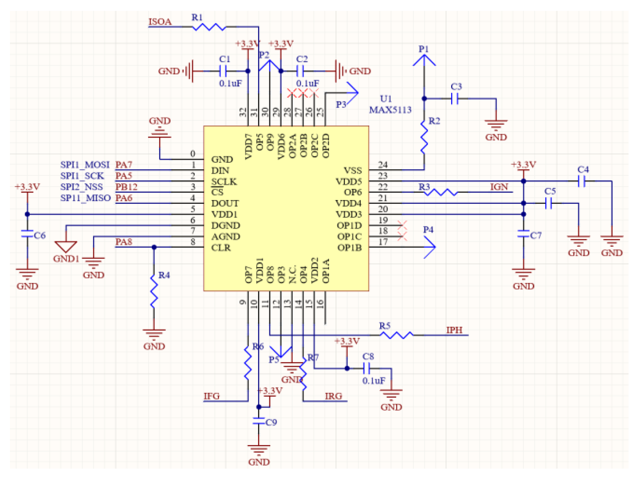
The microcontroller establishes communication with the MAX5113 DAC using a four-wire SPI interface, consisting of the clock line (CLK), data input line (MOSI), data output line (MISO), and chip select line (CS). Through the transmission of specific configuration commands, the microcontroller configures the output currents for each channel of the MAX5113, effectively controlling the semiconductor laser’s five constant current sources. The peripheral circuitry required for the system is relatively straightforward, mainly involving the inclusion of appropriate decoupling capacitors to meet the design requirements of the constant current sources. These capacitors serve the purpose of stabilizing the power supply, filtering unwanted noise, and ensuring reliable operation. To enable accurate current measurements of the five input laser currents, the MAX5113 is connected in series with five high-precision, low-resistance resistors. These resistors convert the actual currents passing through them into corresponding voltage signals. By measuring these voltage signals, it becomes possible to verify the MAX5113’s correct current output and perform fault detection to ensure the device’s proper functionality [31]. Figure 5 provides a detailed depiction of the circuit connections and layout.
In order to meet the 5-channel current requirements of the laser, the MAX5113 DAC is utilized with specific output terminals assigned for different control current types. The OP5 output terminal of the MAX5113 is selected to regulate the control current type for the Semiconductor Optical Amplifier (SOA) current. Similarly, the OP6 output terminal is assigned to control the laser gain current, while the OP8 output terminal is dedicated to controlling the phase current. Additionally, the OP7 output terminal is designated for the control of the front grating current, and the OP4 output terminal is utilized for regulating the rear grating current. This configuration ensures precise and independent control over the various current types necessary for optimal laser performance.
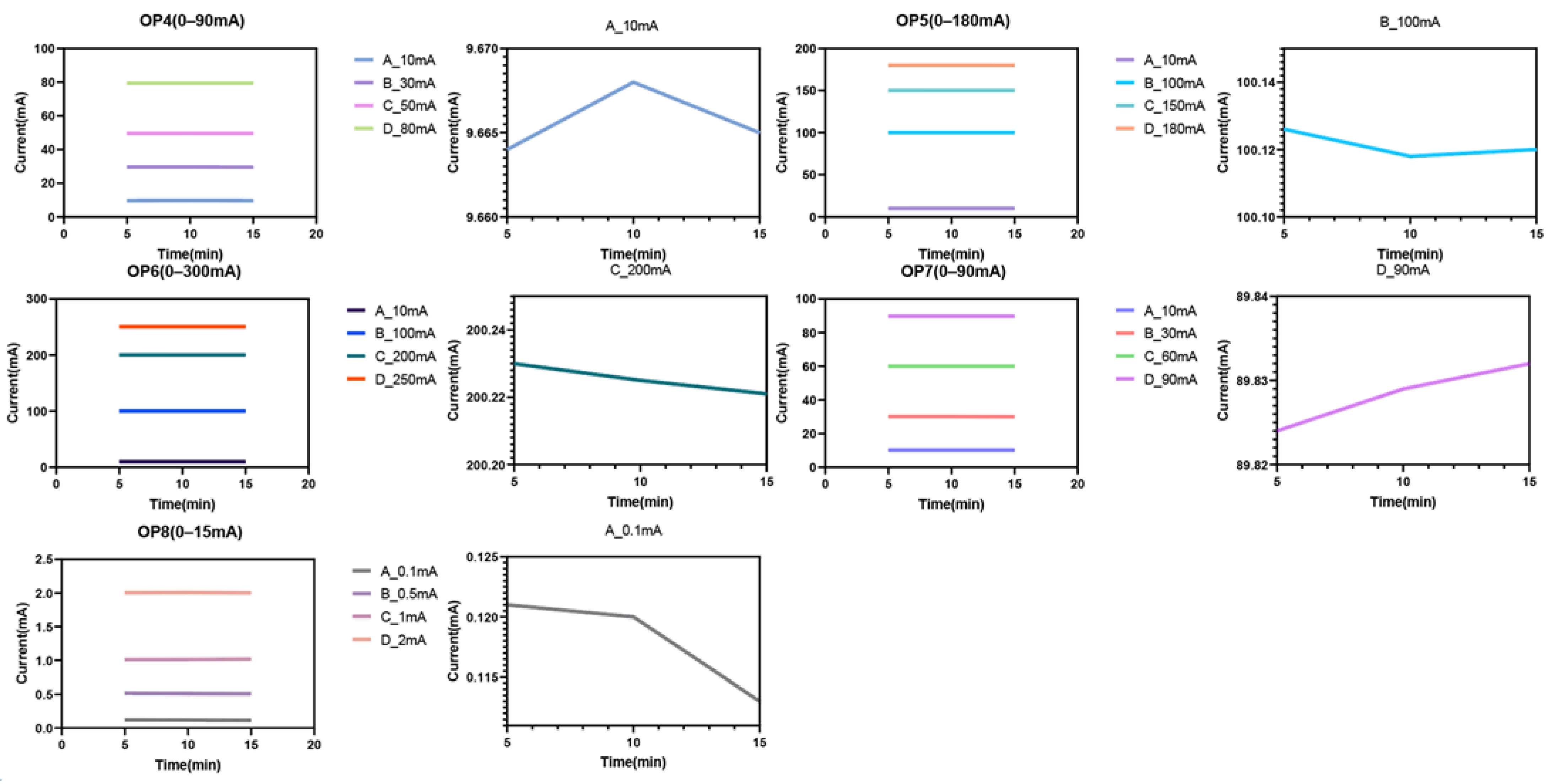
The current output values of the MAX5113 can be configured using a host computer program, allowing for precise control. By conducting a comparative analysis between the host computer’s set values and the actual output values from the circuit board’s constant current source control module, an evaluation of the MAX5113’s performance within the circuit can be performed. To measure the actual output current values of the five channels, a digital multimeter is utilized at regular 5 min intervals, ensuring a comprehensive assessment over a continuous duration of 15 min. Table 2 presents a comprehensive comparison between the host computer’s configured current values for each channel and the corresponding actual output current values, providing valuable insights into the accuracy and reliability of the MAX5113’s functionality within the circuitry. Furthermore, this result is reproducible.
By comparing the measured actual current values with the target current values set by the PC, it can be concluded that the MAX5113 operates normally in the circuit, and the output current is accurate. This confirms that the constant current driving circuit, fabricated with the MAX5113 in this system, can achieve precise control of the five-way input current for the semiconductor laser.
Figure 6 complements Table 2 by presenting a detailed depiction of the actual current values for each channel and their variations over a 15 min duration. During this time period, the maximum error values for the output current of channel OP4, OP5, OP6, OP7, and OP8 are 0.006 mA, 0.008 mA, 0.012 mA, 0.007 mA, and 0.009 mA, respectively. These results indicate that the control circuit exhibits good accuracy and stability in maintaining the desired current levels across all channels. The maximum error values represent the extent of deviation between the actual and target current values for each channel, and these deviations are relatively small. This level of precision ensures reliable and consistent current output performance. The maximum error values further validate the effectiveness and reliability of the designed control circuit, supporting its suitability for demanding applications that require precise current control.
3.3. Temperature Control Circuit Design
Accurate temperature control plays a vital role in achieving stable operation and wavelength tuning in the control system of semiconductor lasers [32]. Semiconductor lasers are susceptible to slight temperature variations caused by external environmental factors and their own thermal effects. These small temperature fluctuations can have a significant impact on the wavelength and power output of the laser. Moreover, excessively low or high temperatures can greatly affect the stability of the system and the accuracy of data measurements. The instability of temperature not only compromises the accuracy of measurement data but can also have adverse effects on the smooth progress of the entire experiment. Therefore, ensuring the stable and reliable operation of semiconductor lasers relies on the implementation of excellent heat dissipation and temperature control systems [33]. A comparative analysis was conducted on the TEC controller series products offered by AD, TI, Wavelength, and MAXIM companies in the field of laser control. Wavelength’s WTC3243 demonstrated the highest precision in temperature control, despite its larger physical size. AD’s AND8830~ADN8834 chips featured a smaller form factor, yet required improvements in temperature control accuracy. TI’s DRV591 and DRV592 necessitated external PWM triggers, adding complexity to the control circuitry. Hence, after comprehensive evaluation, MAXIM’s MAX1978 was selected as the optimal choice. The temperature control circuit of the system employs MAXIM’s MAX1978 chip as the primary component to realize temperature control of the semiconductor laser, guaranteeing its operation at a consistent temperature [34].
The MAX1978 is a fully integrated single-chip temperature controller specifically designed for Peltier thermoelectric cooler (TEC) modules. The chip internally integrates PWM drive circuits, MOSFET drivers, and a PID controller. The direction and magnitude of the drive current vary based on the input temperature difference [35]. PID compensation is achieved using external capacitor and resistor connections. The circuit design is simple and highly integrated. The internal FETs and thermal control loop circuitry not only provide high efficiency but also minimize the need for external components. The switch speed of the integrated MOSFETs has been enhanced to reduce noise and electromagnetic interference. Instead of using voltage-controlled output current, direct control of the output current is employed to eliminate surge currents. The MAX1978 is capable of delivering ±3 A bipolar output, enabling effective temperature control and mitigating dead-zone phenomena. It also addresses nonlinearity issues at light load currents. In the event of a significant independent temperature increase or decrease, it can generate warnings to indicate if the TEC temperature exceeds the normal range. It provides a bias voltage for the thermistor bridge to maintain the on-chip voltage reference in the circuit. The enhanced heat dissipation QFN-EP package with an exposed pad minimizes the operating junction temperature.
In summary, the MAX1978 demonstrates exceptional precision in temperature measurement, facilitating real-time monitoring of the semiconductor laser’s temperature. Given the temperature sensitivity of semiconductor lasers and its direct impact on their performance and longevity, the MAX1978’s high-precision temperature measurement ensures accurate monitoring, effectively safeguarding the laser against overheating or excessive cooling. Notably, the MAX1978 exhibits rapid response characteristics, enabling prompt detection of temperature changes and subsequent implementation of appropriate control measures. Moreover, the integration of multiple protection functionalities, such as overheat protection and temperature alarms, further enhances its reliability. By promptly triggering the necessary protection mechanisms when the laser’s temperature surpasses the configured threshold, the MAX1978 effectively prevents potential damage to the laser. Overall, these outstanding attributes position the MAX1978 as an ideal solution for controlling semiconductor laser circuits in terms of temperature regulation.
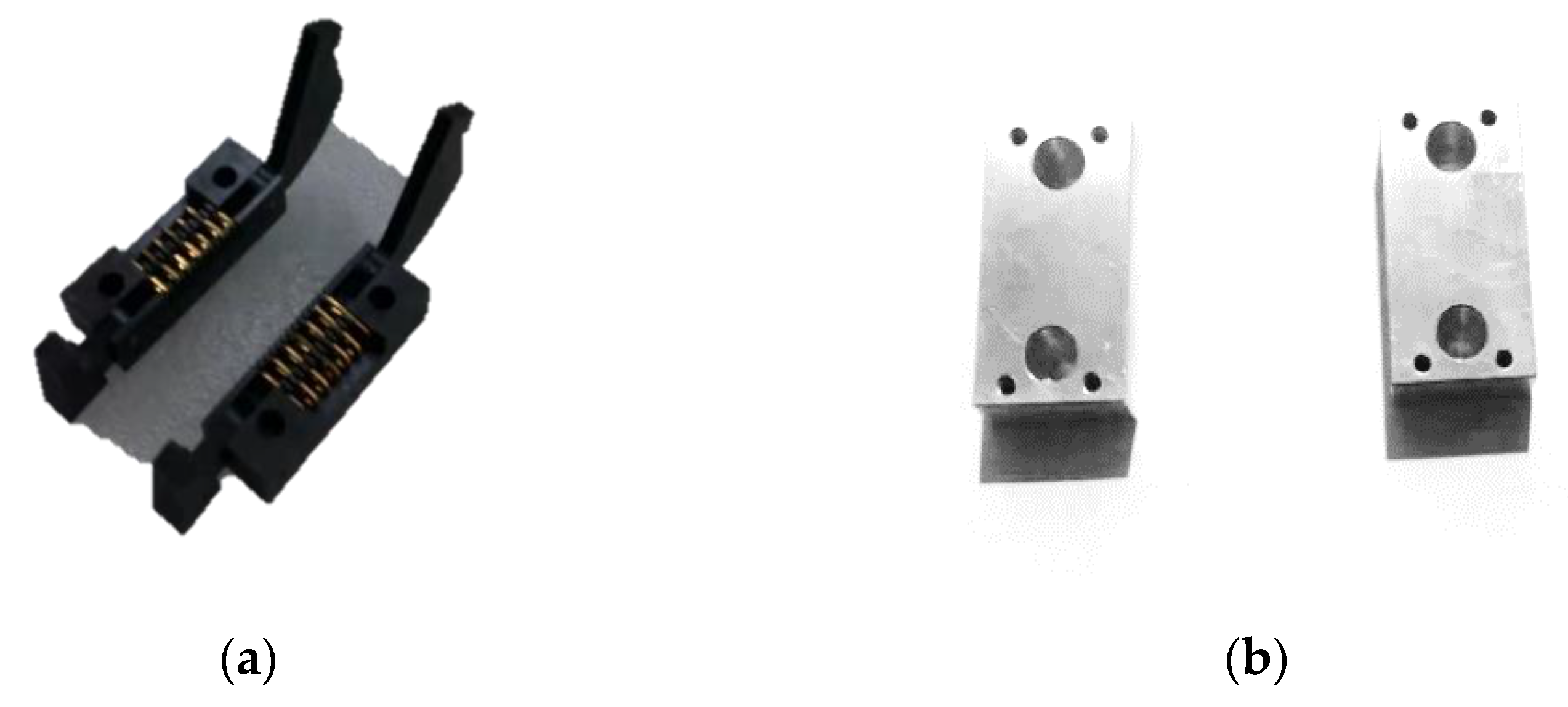
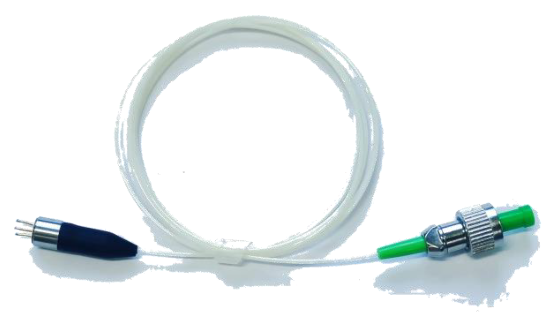
For this design, a butterfly laser fixture and a butterfly laser heatsink drive pad are employed to facilitate the timely dissipation of heat generated by the laser. This provides a secure operating temperature for the laser, ensuring the stability of its output wavelength and optical power. Figure 7 depicts the physical components of the butterfly laser fixture and the butterfly laser heatsink drive pad.
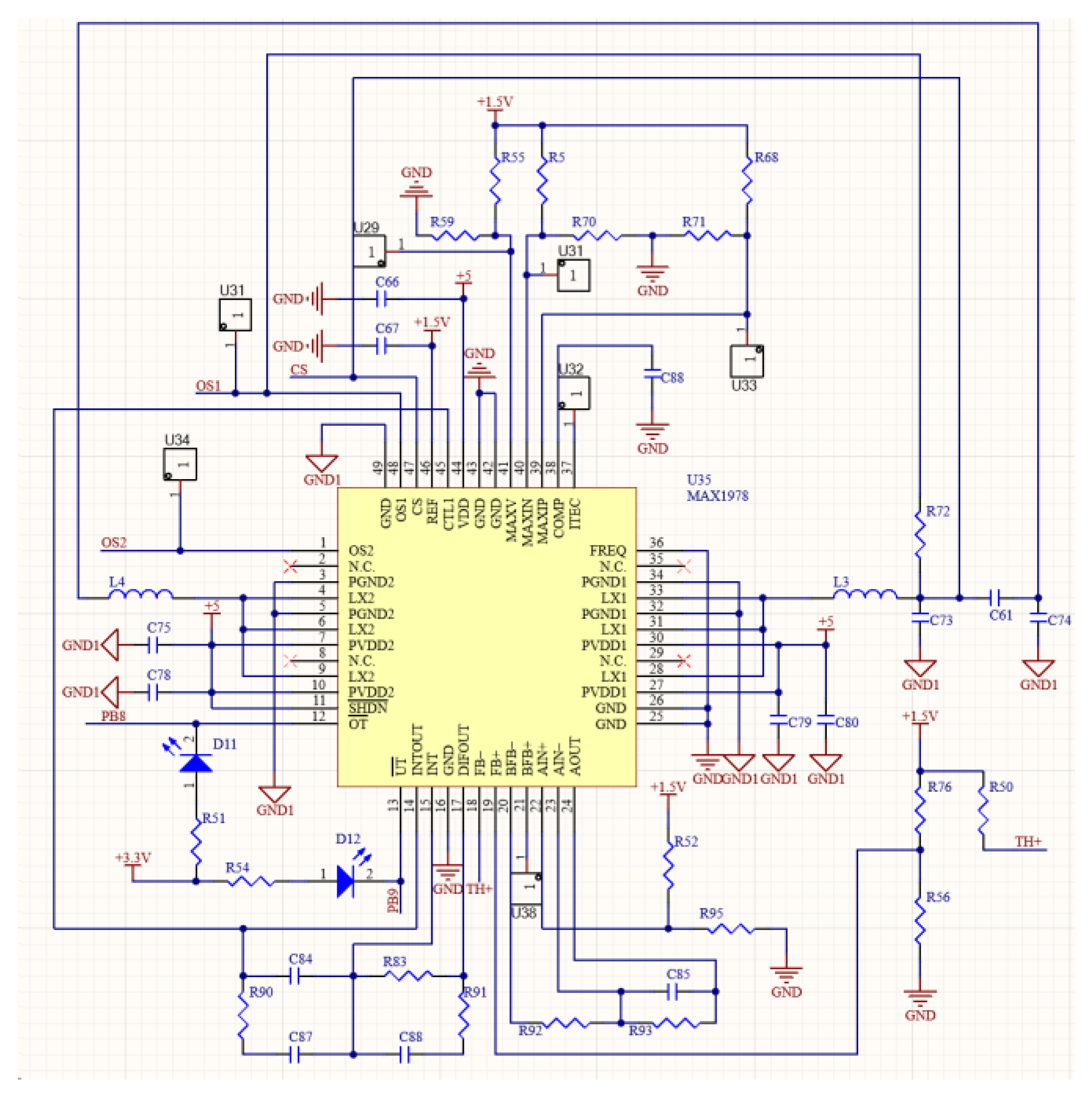
Figure 8 presents the temperature control circuit based on MAX1978. The circuit is divided into three primary sections in terms of functionality: the TEC driver module, the temperature data acquisition and control module, and the PID control module.
The MAX1978 chip allows users to adjust the frequency settings by utilizing the FREQ pin. When the pin is connected to ground, the frequency is set to 500 KHz. When connected to a voltage source, the frequency becomes 1 MHz. The chip incorporates a high-precision +1.5 V reference voltage source, , internally. To adjust the voltages at the MAXV, MAXIN, and MAXIP pins of the MAX1978 chip and regulate the maximum operating voltage and maximum forward and reverse currents of the TEC to protect the internal TEC of the laser, an external resistor can be used for voltage division. Pin 41 (MAXV) of the chip can be configured to set the maximum voltage across the TEC. The following formulas can be utilized for this purpose. The formula is shown in Equations (1) and (2):
Through reference to the laser chip manual, the control requirements related to the thermoelectric cooler (TEC) used in the laser device can be determined. These specifications are essential for establishing the upper limit of the heating/cooling voltage, denoted as , required for efficient TEC operation, as well as the voltage, , applied to the MAXV pin. By employing Equations (1) and (2), it becomes feasible to compute the precise resistance values for R59 and R55, which are pivotal in attaining the desired TEC control parameters.
The VMAXIP and VMAXIN pins are used to set the maximum forward and reverse currents passing through the TEC. The maximum forward current, , and the maximum reverse current, , can be obtained using Equations (3) and (4), respectively.
A microresistor, denoted as , is interconnected between the CS and OS1 pins, serving as a means to regulate the current passing through the thermoelectric cooler (TEC) by carefully selecting an optimal value for . The utilization of Equations (3) and (4) facilitates the determination of precise resistance values for R71, R68, R70, and R5.
The pins 12 () and 13 () of the MAX1978 chip serve as alarm indicators for high or low temperature conditions. When the voltage difference between pins 18 (FB−) and 19 (FB+) exceeds 20 mV, either pin 12 () or pin 13 () is pulled low. Two light-emitting diodes (LEDs) are connected externally to pins 12 and 13. During heating or cooling operation of the TEC, the corresponding LED will be illuminated, providing a visual indication of the TEC’s operational status. This configuration enables quick assessment of the TEC’s performance by monitoring the LED states in different operating modes.
Pin 18 (FB−) and Pin 19 (FB+) of the MAX1978 chip are connected to the real-time temperature voltage and user-set temperature voltage of the laser, respectively. The FB− pin reflects the real-time temperature of the laser, which is determined by the resistance value of the internal thermistor in the laser (with a resistance of 10k at room temperature). The FB+ pin represents the user-set temperature voltage for the laser. The FB+ and FB− pins form a resistor bridge, consisting of the thermistor on the laser chip and an external 10k resistor, to obtain the voltage signal related to the chip temperature. By default, when the voltage on the FB+ pin is 0.75 V, the working temperature of the TEC is considered to be 25 °C. When there is a temperature difference between the internal temperature and the set temperature of the laser, the temperature difference circuit outputs a non-zero value. Depending on the polarity of the voltage, the driving current direction for the Thermoelectric Cooler (TEC) is determined, controlling the TEC driver to stop heating or cooling [36]. Furthermore, the magnitude of the voltage difference also determines the efficiency of the heating or cooling operation. A larger voltage difference leads to higher heating or cooling efficiency. When the voltage difference across the TEC is 0 V, it indicates a very small temperature difference or a state close to equilibrium. In such cases, the TEC driver stops the heating or cooling operation to maintain temperature stability.
The PID temperature compensation network plays a crucial role in TEC temperature control, exerting a significant influence on the response speed and control accuracy of the entire temperature control module. To ensure stability, speed, and minimal error in the temperature regulation process, it is essential to set the parameters of the PID circuit appropriately. This involves adjusting the values of capacitors and resistors between four pins of the MAX1978 chip: Pin 14 (INTOUT), Pin 15 (INT-), Pin 17 (DIFOUT), and Pin 45 (CTRI). Through calculations and practical experience, the parameters are tuned, and the design employs the resistor and capacitor values provided as references in the MAX1978 datasheet for Pin 14, 15, 17, and 45.
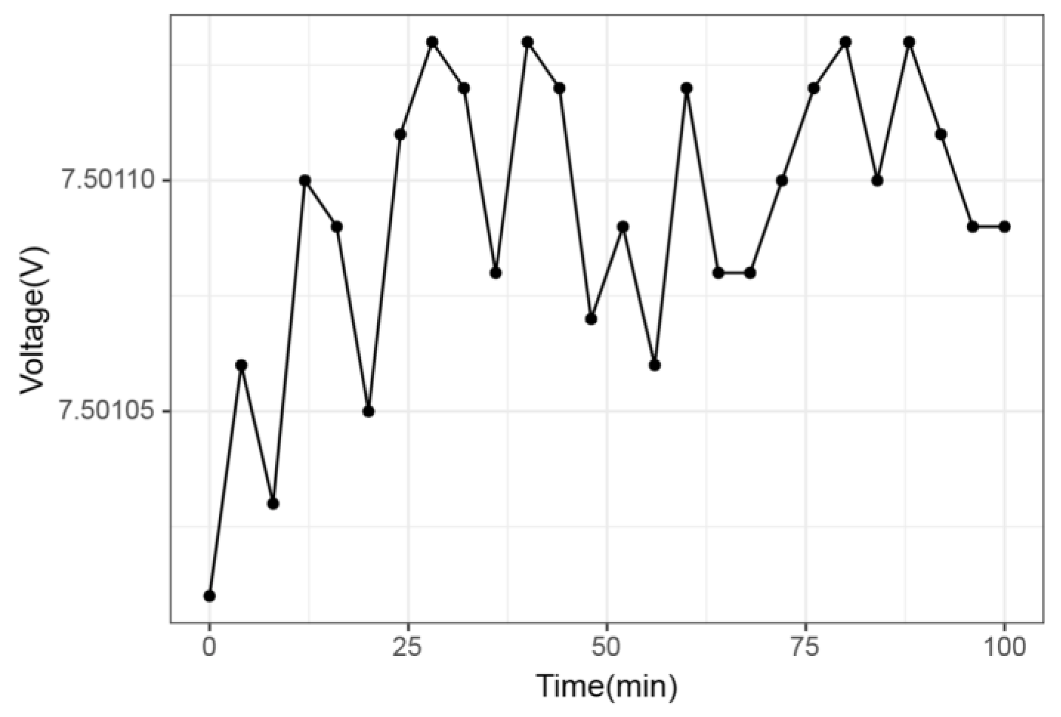
During the testing experiment, the laser temperature was set to 25 °C. Using a digital multimeter, the voltage at the FB− point (TH+ point) of the temperature control circuit, which corresponds to the voltage division across the internal thermistor of the laser, was measured every 4 min. A total of 100 min of continuous measurements were taken. Within the 100 min duration, the maximum change in voltage at the FB− point was 0.12 mV, as illustrated in Figure 9. There were no specific requirements for temperature range, voltage, or noise environment in this experiment.
The experiment provides information about the stability and accuracy of the temperature control circuit at the given temperature. By measuring the variation in voltage at the FB− point, the performance of the temperature control circuit can be evaluated, and its effectiveness in maintaining laser diode temperature stability can be verified.
3.4. Optoelectronic Detector Circuit Design
A photodetector is an optoelectronic device that converts light signals into electrical signals. The working principle of a photodetector is based on the photoelectric effect, where the absorption of light energy leads to electron excitation and charge release. Photodetectors can be classified into various types based on different principles and materials, including photodiodes, photomultiplier tubes, phototransistors, and photoresistors. Photodetectors are characterized by their high sensitivity, fast response, wide wavelength range, and low noise. Depending on the specific application requirements, photodetectors can operate in different modes such as single-photon detection, continuous wave detection, and pulse detection. Additionally, photodetectors can incorporate functions such as gain adjustment, filtering, and temperature compensation as needed. In practical applications, photodetectors are often used in conjunction with other optical components, such as lenses and filters, as well as electronic devices like amplifiers and A/D converters, to facilitate the acquisition, processing, and analysis of light signals. They play a crucial role in areas such as spectroscopy, optical communications, light measurement, and optical imaging.
A photodetection circuit generally consists of two main parts: photodetection conversion and photonic signal acquisition. These two parts play crucial roles in the reception, conversion, and processing of light signals. The photodetection part is the core of the photodetection circuit, responsible for converting the light signal from the light source into a corresponding electrical signal. This part typically includes photodiodes, phototransistors, photomultiplier tubes, or other appropriate optoelectronic devices selected based on specific application requirements. These optoelectronic devices utilize principles such as light energy absorption and the photoelectric effect to generate electron excitation and charge release, thereby converting light energy into electrical energy. The photonic signal acquisition part is responsible for amplifying, filtering, and adapting the electrical signal output from the photodetection part, enabling subsequent processing and analysis by electronic devices. This part usually includes amplifiers, filters, A/D converters, and other electronic components that enhance signal strength, eliminate noise interference, and convert analog signals into digital signals for further digital signal processing.
The design and optimization of the entire optoelectronic detection circuit aim to achieve high sensitivity, fast response, wide wavelength range, and low noise characteristics. Therefore, the selection includes an InGaAs material photodiode and a transimpedance amplifier, the HA1004. Figure 10 is a physical diagram of the photodiode in the optoelectronic detector.
The photodetector diode used in this system exhibits excellent reliability, covering a wide range of response wavelengths in the C-band, and has low dark current and low power consumption levels. The optical sensor receives the light signal and converts it into a small current, which is then converted into a voltage signal from the output current of the photodiode through a transimpedance amplifier (TIA). The voltage signal is then processed by an A/D converter and handled by an MCU.
The HA1004 is a domestically developed analog integrated circuit, designed by Shenzhen Qianhong Microelectronics Co., Ltd. (Shenzhen, China), featuring a four-channel Transimpedance Amplifier (TIA) with input clamp protection. Specifically designed for optoelectronic detection at the front-end, it serves as an excellent choice for domestically produced chips in optical sensor applications. The HA1004 integrates four channels of TIA amplifiers, multiplexers, and differential buffers. With its programmable gain modes (5k, 15k, 30k, and 50k), the TIA amplifier eliminates the need for subsequent amplification stages, offering dynamic selection capabilities. Its low noise coefficient of 4 pA√Hz significantly extends the working distance, effectively amplifying weak signals received by photodetectors. Given that photodetectors typically generate small signals, amplification is necessary to obtain usable outputs. The HA1004 ensures effective amplification of weak signals, thanks to its high gain and wide bandwidth, enabling the handling of high-speed signals as well. Throughout the signal amplification process, the HA1004 maintains low noise and distortion levels. The low noise enhances the signal-to-noise ratio, enabling photodetectors to capture and analyze light signals more effectively. Additionally, the low distortion preserves signal accuracy and integrity, thereby enhancing measurement precision. The HA1004 offers flexible options for power supply voltage and current configurations, allowing adjustments to meet specific application requirements. This adaptability enables the HA1004 to accommodate different operating conditions and characteristics of various photodetectors, guaranteeing optimal performance and adaptability.
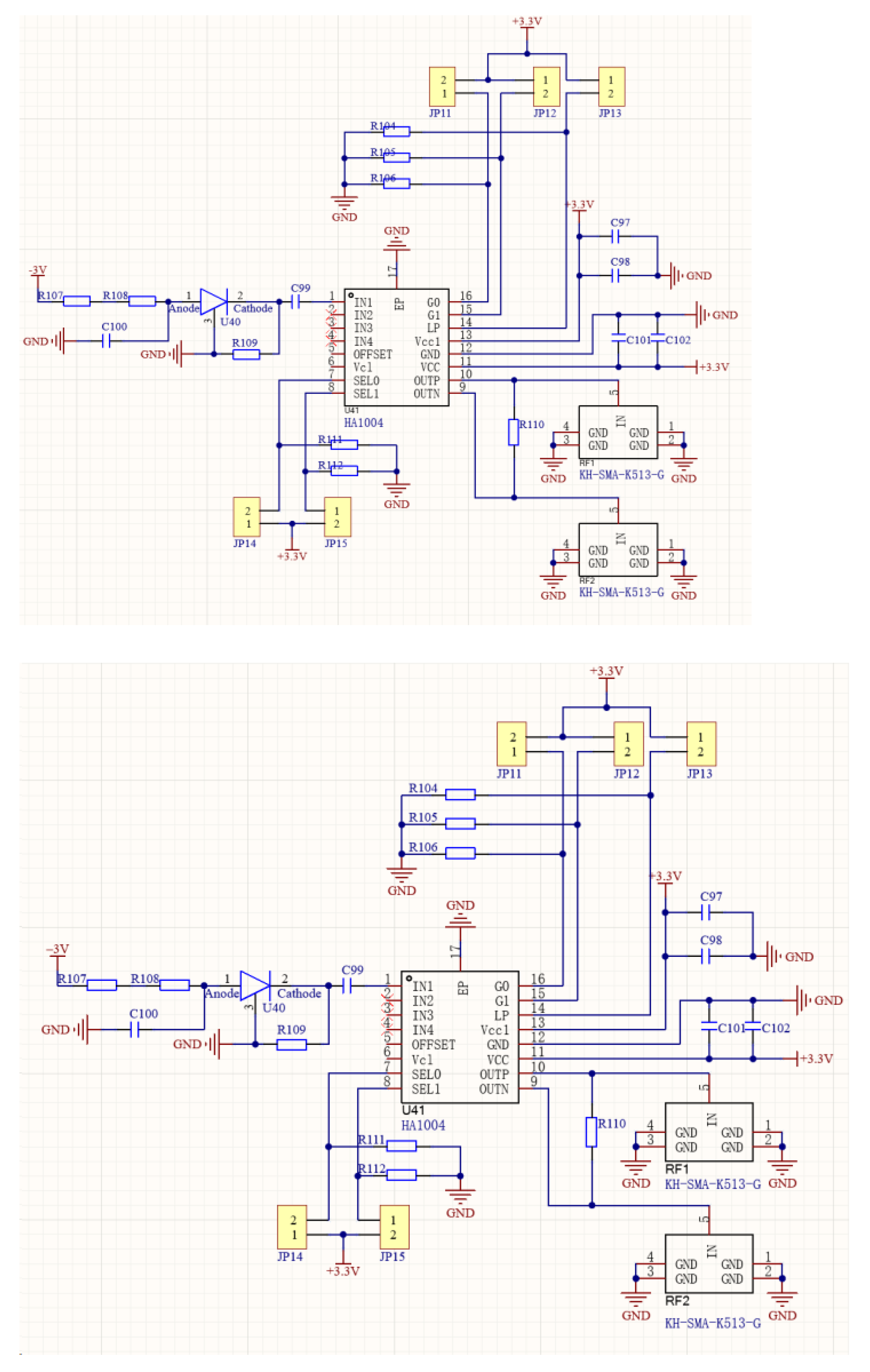
During circuit design, compensation capacitors are reserved to prevent insufficient phase margin and signal distortion. Figure 11 shows the schematic diagram of the photodetector, combining the photodiode front-end circuit with the HA1004 transimpedance amplifier.
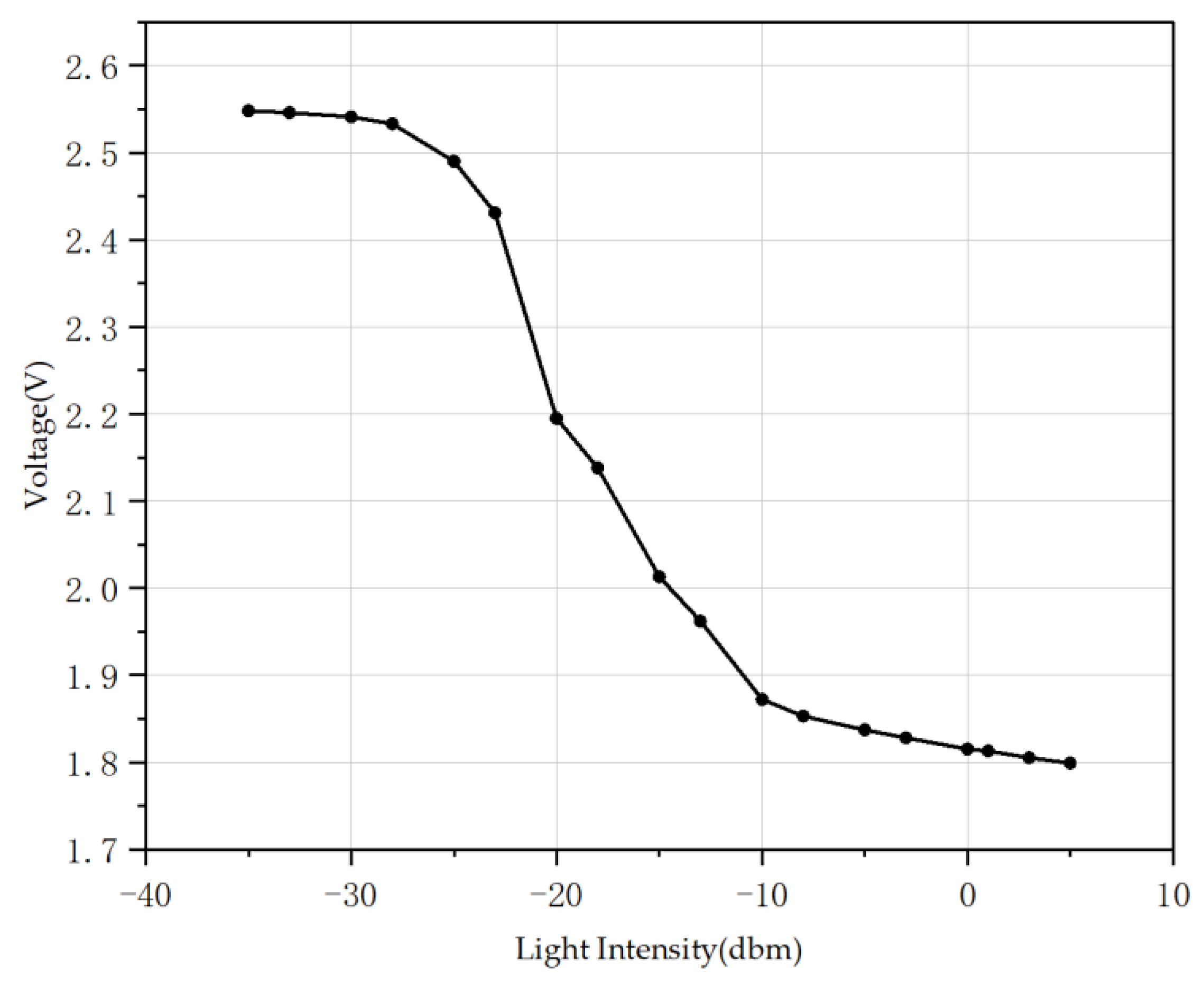
In the experiment aiming to calibrate the relationship between optical power and detector voltage in a point-by-point manner, a broadband optical source was utilized for detector calibration. The calibration process involved gradually increasing the input optical power and measuring the corresponding changes in the output signal. The saturation optical power was determined by adjusting the attenuation and observing the voltage response. The linearity dynamic range was assessed by evaluating the linearity between the detector’s output signal and the input optical power. The output voltage of the photodetector was measured using a digital multimeter. The experimental results indicated saturation of the circuit at approximately +5 dBm. However, the measurement range can be adjusted by modulating the input voltage and resistors at the hardware level. The HA1004 provides gain modes, including 5k, 15k, 30k, and 50k, where higher gain results in a narrower adjustable range. Figure 12 shows the trend graph of the output voltage variation with the magnitude of light intensity.
3.5. AD Conversion Module Design
In this design, the AD7798 chip is employed as the A/D conversion module due to its superior capabilities in terms of resolution and accuracy when compared to the A/D conversion module integrated within the STM32F103 microcontroller. The A/D conversion circuit, responsible for the transformation of continuously varying analog signals into their corresponding digital counterparts, plays a crucial role. Analog signals denote continuous waveforms with variable magnitudes confined within a defined range, while digital signals are discrete representations portrayed by a series of numerical values. The output voltage of the photodetector is precisely converted into a digital signal utilizing a high-precision A/D conversion module. These precise digital signals are subsequently transmitted to the core microcontroller via SPI for subsequent processing and analysis. This design ensures the accurate and dependable comprehension and processing of the photodetector’s voltage values by the microcontroller, enabling proficient acquisition and utilization of the photonic signals, thereby facilitating efficient handling and utilization of the acquired data.
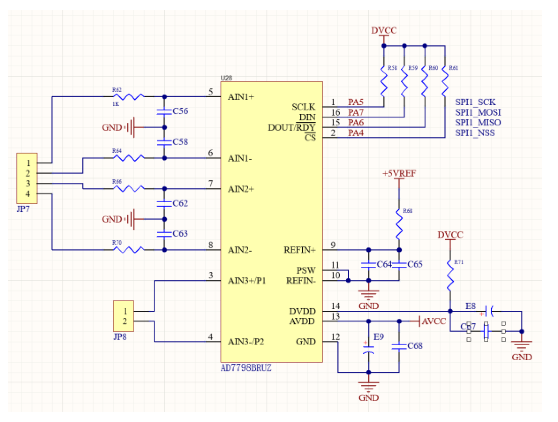
The AD7798 is a chip specifically designed for high-precision measurement applications, featuring low power consumption, low noise, and a complete analog front end. It integrates a 16-bit/24-bit Σ-Δ ADC with three differential analog inputs, enabling accurate signal conversion. Additionally, it incorporates a low-noise instrumentation amplifier, allowing direct input of small signals. When set to a gain of 64 and an update rate of 4.17 Hz, the AD7799 exhibits a root mean square (RMS) noise of 27 nV, while the AD7798 has an RMS noise of 40 nV. This indicates its capability to provide extremely accurate and reliable measurement results. The chip also integrates several features internally, including a low-power switch, reference voltage detection, programmable digital output pins, fuse current control, and an internal clock oscillator. Moreover, software programming allows for adjustment of the output data rate, ranging from 4.17 Hz to 470 Hz. With a typical power consumption of 300 µA, the AD7798 demonstrates a significant advantage in applications requiring high measurement accuracy and precise analog signal conversion. Whether in precision measurement, instrument equipment, or sensor calibration, the AD7798 delivers outstanding performance and reliability, meeting stringent requirements for high-precision measurement. The circuit diagram of the AD7798 is depicted in Figure 13.
3.6. Serial Communication Circuit Design
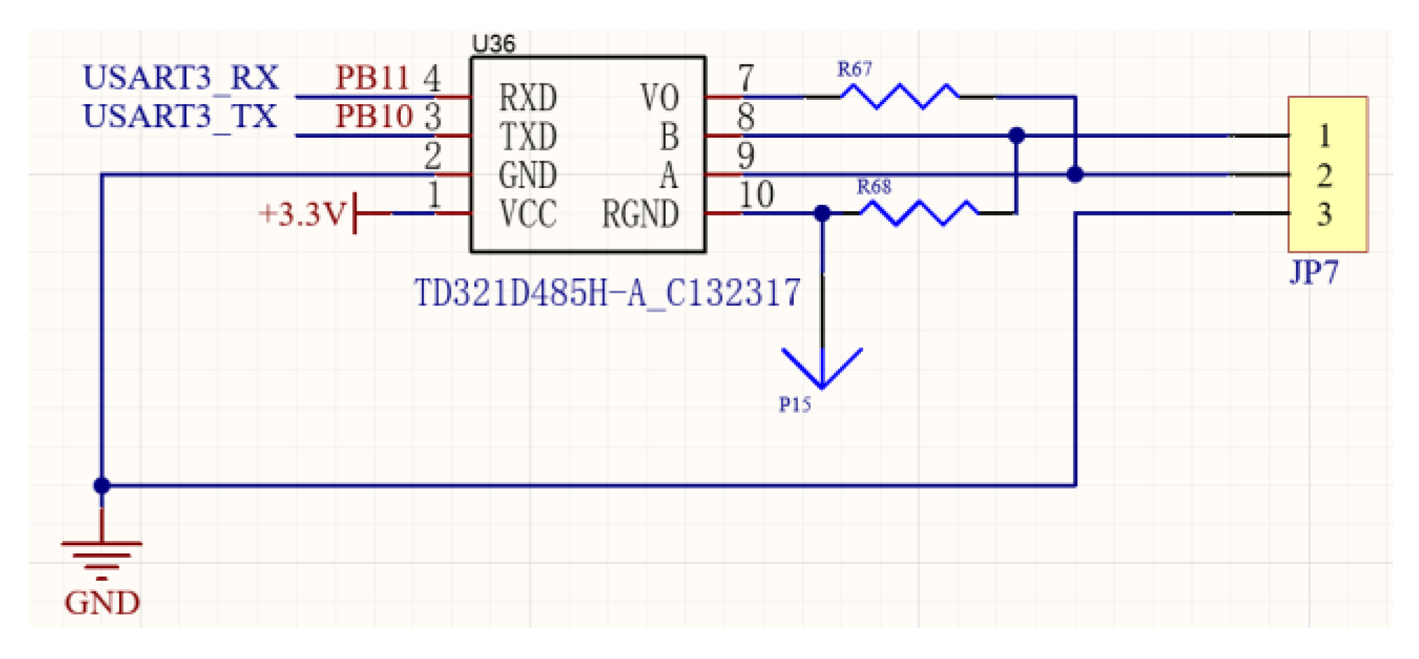
Serial communication serves as a prevalent approach for facilitating data transmission and device control, establishing a streamlined and dependable communication channel between computers and external devices. Its indispensability spans across diverse domains encompassing data transfer, device manipulation, monitoring, debugging, and communication with embedded systems. In this design, the communication functionality between the microcontroller and the host computer is realized through the utilization of the TD321D485 module in conjunction with a USB to RS485 serial cable. This integration facilitates seamless data interchange, precise device control, and comprehensive system monitoring within the microcontroller ecosystem. The serial port serves as the conduit through which imperative instructions, vital data, and critical status information can be conveyed to the microcontroller system, while simultaneously enabling the receipt of prompt and pertinent responses emanating from the microcontroller system.
The TD321D485 module is an advanced RS485 protocol transceiver that seamlessly integrates power isolation, signal isolation, RS485 communication, and bus protection functionalities. It incorporates an embedded regulated isolation power supply, enabling robust electrical isolation of up to 3000 VDC. This exceptional electrical isolation effectively mitigates potential power and ground interference among interconnected devices, thereby elevating system stability and reliability. Moreover, the module adeptly performs the vital task of logic level to differential level conversion, a requisite for seamless compatibility with the RS485 protocol, thereby ensuring efficient signal isolation. By leveraging this signal isolation mechanism, the module effectively neutralizes the deleterious impact of interference and noise during signal transmission, thereby bolstering signal reliability and augmenting its anti-interference capabilities. The TD321D485 module boasts extensive support for the widely adopted RS485 communication protocol, which finds particular utility in long-range and multi-node communication scenarios. Its impressive anti-interference capabilities, coupled with its long transmission distance and capacity for accommodating multiple nodes, render it particularly well-suited for deployment in industrial automation and Internet of Things (IoT) applications. Furthermore, the module incorporates robust bus protection mechanisms, effectively shielding the RS485 bus from potential damage stemming from external power interference, electrical shocks, or other adverse factors. The diligent implementation of bus protection measures ensures unwavering communication stability, reliability, and significantly prolongs the operational lifespan of interconnected devices.
Figure 14 depicts the design of the serial communication circuit. With the system operating at a 3.3 V power supply, the TD321D485 chip from MORNSUN Guangzhou Science & Technology Co., Ltd. (Guangzhou, China) is selected. The VCC and GND pins of the TD321D485 module are connected to the power and ground pins, respectively, of the STM32F103 microcontroller. The A+ and B− pins of the TD321D485 module are connected to the A+ and B− lines of the RS485 bus. The TX and RX pins of the TD321D485 module are connected to the serial port pins of the STM32F103 microcontroller, typically with the TX pin linked to the RX pin of the microcontroller’s serial port and the RX pin connected to the TX pin of the serial port.
3.7. Power Supply System Design
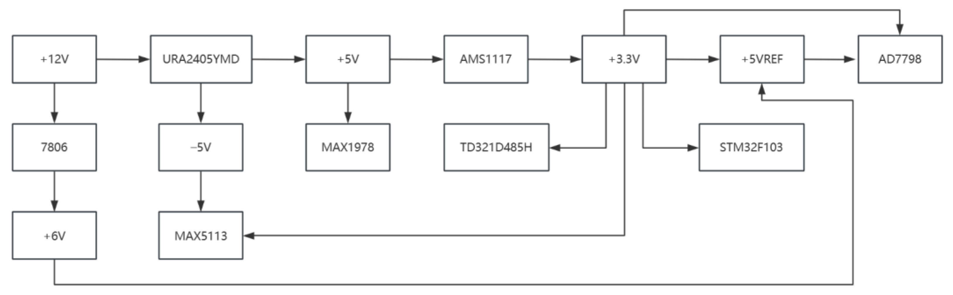
Power supply design is an indispensable part of the entire system, providing the required energy to various modules within the system. The microcontroller’s minimum system operates at a power supply voltage of 3.3 V. A voltage regulator (such as a linear regulator or a switching regulator) is employed to deliver a stable power source. Ample filtering capacitors should be added at the input and output ends to reduce noise and ensure a stable power supply.
In this design, we have employed the AMS1117-3.3 V low-dropout linear regulator. The AMS1117-3.3 V is renowned for its exceptional precision in maintaining a stable output voltage. It reliably regulates the input voltage to a steady 3.3 V, exhibiting minimal output voltage drift and ripple. This remarkable precision ensures the optimal functioning of other electronic components within the system while providing a consistent and reliable power supply. Furthermore, the AMS1117-3.3 V boasts low power consumption characteristics. Its design incorporates a low quiescent current, resulting in negligible static current draw under light load conditions. This attribute holds particular significance for applications emphasizing energy efficiency and prolonged battery life. Additionally, the AMS1117-3.3 V is a highly integrated power chip that internally integrates functionalities such as a voltage reference source. This integration capability streamlines the design process, reduces the reliance on external components, and enhances overall system reliability.
The temperature control module is supplied with a +5 V voltage, while the constant current source receives power from both −5 V and 3.3 V sources. The ±5 V DC/DC module power supply from MORNSUN Guangzhou Science & Technology Co., Ltd. This power module exhibits a 10 W output power, an ultra-wide voltage input range of 4:1, and an impressive efficiency of up to 88%. It is equipped with a standard isolation voltage of 1500 VDC and incorporates protective features such as input undervoltage protection as well as output overvoltage, overcurrent, and short circuit protection mechanisms.
The AD7798 is powered by +5 VREF and 3.3 V together, and the serial communication circuit operates at a 3.3 V voltage level. During the circuit board design process, careful attention should be paid to the layout and routing of power lines to minimize interference and voltage drop. Separating power lines for different functional modules helps reduce mutual interference. Figure 15 provides an overview of the power supply modules for each major component.
3.8. PCB Layout and Routing Design
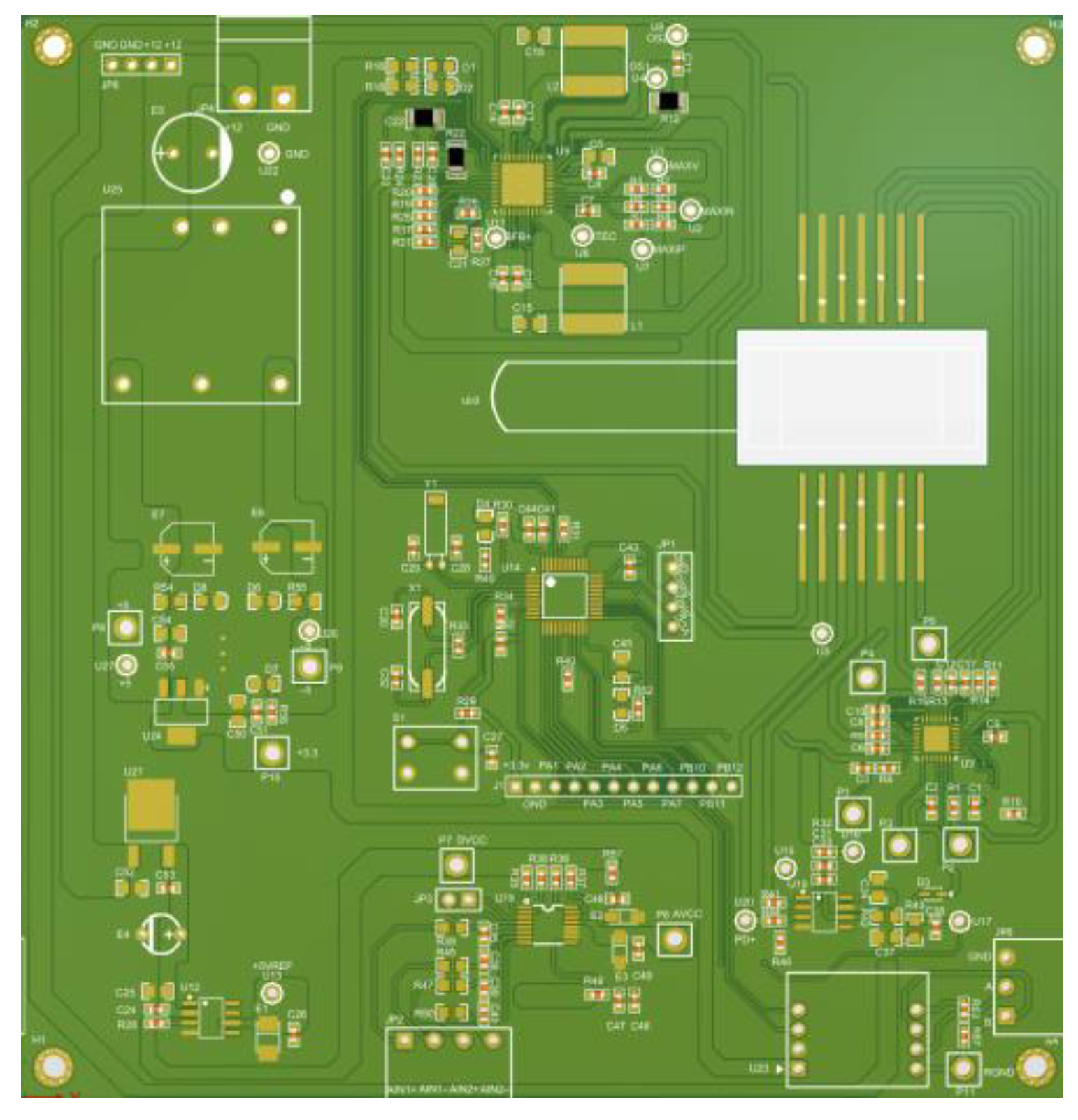
Based on the aforementioned circuit designs for the constant current driver, temperature control, optoelectronic detection, AD conversion module, power supply system, and serial communication system, it is advisable to minimize the length of signal lines as much as possible during PCB layout and design to reduce signal transmission loss and interference. Sufficiently wide copper traces should be used for the constant current source and TEC output sections to withstand high currents. According to the requirements of the serial communication system, ensure that signal lines are routed short and straight to minimize interference and signal transmission loss. Differential signal lines can be used to improve the anti-interference capability of the serial communication. Ensure that the routing of differential signal pairs on the PCB is well-matched and maintain equal lengths. Optimize the routing of signal lines and ensure that the paths are clean and direct. Separate high-power and low-power circuits to reduce mutual interference. Lay out high-power components (such as the constant current source and TEC) separately from low-power components (such as signal processing circuits) to prevent interference propagation. Use ground planes and power planes to provide effective grounding and power distribution, reducing signal return paths. Ensure good connections between the ground and power planes and relevant circuits to minimize electromagnetic interference and noise. Maintain sufficient spacing and isolation to prevent interference and cross-talk between different circuits. Aim to keep distances between circuits and minimize interference between signal and power lines. Start by outlining the framework of the circuit, determining the approximate positions and orientations of each module, and then gradually refine the routing to ensure logical, compact, and well-routed connections. Figure 16 presents the hardware PCB layout of the system circuit board.
4. Analysis of Result
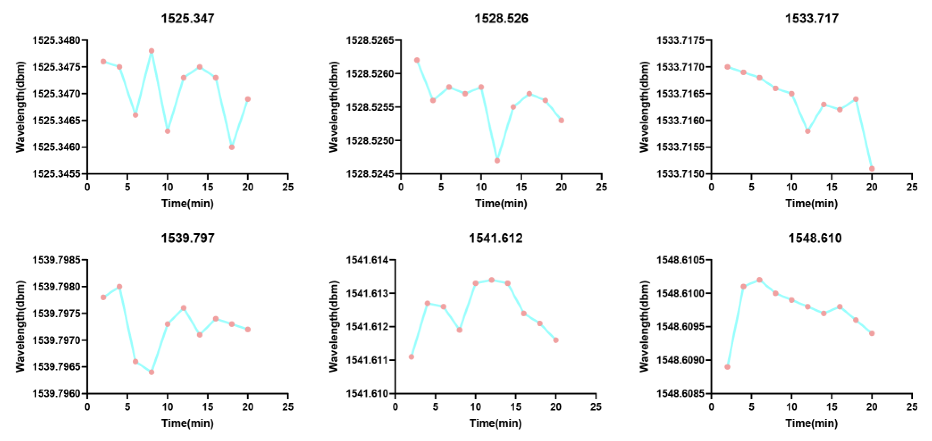
To validate the exceptional wavelength stability of the laser, we employed an Agilent 86122A optical wavelength meter with a wide range of 1270 nm to 1650 nm for conducting the wavelength stability tests. The testing process was conducted without any specific experimental constraints. The output fiber from the laser was connected to the input port of the optical wavelength meter. Subsequently, the wavelength meter software was activated, and the system underwent initialization and calibration procedures. Within the 1525 nm to 1550 nm range, six specific wavelength points were carefully selected for testing: 1525.382 nm, 1528.555 nm, 1533.748 nm, 1539.859 nm, 1541.663 nm, and 1548.65 nm. The upper computer precisely controlled the laser to emit light at a wavelength of 1525.382 nm, while the optical wavelength meter continuously monitored and captured the real-time output wavelength of the laser. Data was meticulously recorded at two-minute intervals, with ten measurements obtained for each wavelength point, resulting in a comprehensive duration of 20 min. Upon completing the data collection process for 1525.382 nm, the aforementioned procedure was repeated for each subsequent wavelength point, including 1528.555 nm and so forth, until all six wavelength points were thoroughly examined. The detailed results of the conducted tests are presented in Table 3.
From the data presented in the above table, it is evident that the laser exhibited wavelength drift within 3 pm or even maintained stability at the specified wavelength during the 20 min duration. Additionally, a random trend of wavelength variation can be observed, with fluctuations occurring unpredictably within the 3 pm range. Further measurements were conducted for each wavelength point, extending the duration to 1 h, and the increased volume of available data reaffirmed the random nature of wavelength changes. It was observed that even with a constant driving current, the wavelength could still undergo variations, and these changes were also influenced by temperature. Unfortunately, prolonged operation did not lead to any improvement in the observed wavelength variations.
Figure 17 complements Table 3 by presenting a concise line graph illustrating the variations of each wavelength value within the 20 min duration. The laser’s actual output values may closely approximate the set value but exhibit a certain wavelength offset. This offset can be attributed to factors such as inherent laser characteristics, external temperature fluctuations, fluctuations in the driving current, or other influencing factors. In many applications, a wavelength variation of up to 3 pm is considered within an acceptable range. Analysis of the data from Figure 17 and Table 3 confirms the pivotal role played by the constant current source and temperature control circuitry in ensuring the laser’s stable operation. These results further authenticate the effectiveness, reliability, and stability of the employed constant current source and optical source temperature control system in practical applications.
5. Discussion
This study presents the design of a tunable laser control circuit based on the STM32 microcontroller. The circuit comprises various modules, including the power supply module, core microcontroller, constant current control module, temperature control module, ADC conversion module, photodetector module, and RS485 serial communication module. Additionally, the photodetector and ADC conversion modules can also serve as the foundation for a fiber optic grating demodulation system.
First of all, a comprehensive system assessment was conducted, and suitable integrated circuits were meticulously selected for each module. The power supply module incorporates chips proficient in providing bipolar power supply and harmonizing them with chips delivering +6 V and +3.3 V outputs. The central microcontroller opted for was the STM32F103, though, for augmented system performance, a more advanced microcontroller chip could be contemplated. The constant current control module and temperature control module leverage the MAX5113 and MAX1978 chips, respectively, from the esteemed Maxim Integrated. The ADC conversion module employs the AD7798 chip, with the potential for future replacement with a chip offering superior resolution and numerical accuracy should heightened performance requisites emerge. The photodetector module embraces the HA1004 chip sourced from Shenzhen Qianhong Microelectronics Co., Ltd. For RS485 serial communication, a single-channel high-speed RS485 isolation transceiver module endowed with automatic transmission and reception switching is employed.
Moreover, subsequent to the completion of each module’s design, meticulous experimentation was conducted to scrutinize the conformance of each module to the designated performance requirements. The ultimate outcomes reveal the following:
- The MAX5113 control circuit exhibits remarkable precision and stability in effectively regulating the desired current levels across all channels, showcasing a maximum error value of a few microamperes. This exceptional performance surpasses the capabilities of conventional discrete constant current sources by a significant margin.
- The MAX1978 control circuit demonstrates exceptional stability with negligible temperature voltage fluctuations, maintaining a range of only a few tens of microamperes over a 100 min duration. In comparison to employing chips from TI, the utilization of the MAX1978 chip showcases superior compatibility with the power supply and driving current requirements of the majority of TEC models. Furthermore, the circuit design is straightforward and exhibits a high degree of integration. The superiority of this design approach over alternative solutions is substantiated by empirical evidence derived from rigorous experimentation.
- According to the laboratory data, the performance of the photodetector circuit, ADC circuit, and power supply system satisfactorily fulfills the experimental requisites.
- The laser output wavelength range is within 1525 to 1550 nm, with wavelength fluctuations within 3 pm.
The wavelength range of 1525 to 1550 nanometers holds significant importance and finds widespread applications in the fields of optical fiber communication and optical fiber sensing. Within this range, fiber attenuation is minimized, and fiber non-linear effects are relatively negligible, enabling long-distance transmission and high-speed data transfer. Signal transmission in most optical fiber communication systems is achieved through the use of the 1525 to 1550 nanometer wavelength range. Optical fiber sensing technology utilizes variations in optical signals within the fiber to detect and measure environmental parameters such as temperature, pressure, and strain. In these applications, the 1525 to 1550 nanometer wavelength range is commonly employed for laser wavelength output, often in conjunction with sensor-integrated fiber systems. Lasers with wavelength fluctuations of less than 3 pm are highly sought after in practical applications that require precise wavelength control and stability, including fiber sensing, spectral analysis, and photonics experiments. Wavelength stability is crucial for reliable demodulation of information and plays a key role in ensuring the overall system’s reliability. Experimental results in laser control circuitry have verified the circuit’s ability to maintain a stable wavelength emission from the laser. By integrating it with fiber Bragg grating (FBG) and Fabry–Pérot (FP) sensors, more reliable data and information regarding environmental factors can be obtained.
Overall, the study successfully designed and evaluated the tunable laser control circuit, verifying its accuracy and performance through experiments. However, the current research is limited to a specific wavelength range, and it would be advantageous to explore the expansion of the system’s wavelength range to cater to a broader spectrum of optical communication applications and requirements in the future. This expansion may necessitate the optimization and adjustment of lasers for different wavelengths to ensure wavelength stability and reliable demodulation adaptability. Furthermore, the hardware system utilized in this experiment can be further integrated and optimized to mitigate the 3 pm wavelength fluctuation through hardware adjustments.
6. Conclusions
After comprehensively investigating the tuning characteristics of the laser, the overall scheme for the laser control system was decisively formulated. In this scholarly article, an STM32 microcontroller-based laser control circuit was meticulously devised, concurrently facilitating the seamless integration of the fiber Bragg grating demodulation system. This ingeniously engineered circuit enables precise wavelength output of the laser within the esteemed range of 1525 to 1550 nm, while showcasing an impressively low maximum fluctuation rate of merely 3 pm. The ingenuity of the design lies in the astute utilization of the MAX5113 high-precision current source chip and the MAX1978 temperature control chip, synergistically employed to impeccably drive and meticulously regulate the semiconductor laser. The judicious integration of these cutting-edge chips ensures an indomitable control over the laser’s current and temperature, thereby unequivocally guaranteeing its unparalleled performance and unwavering stability.
In addition to achieving continuous current adjustability and ensuring the stable operating temperature of the laser, the circuit devised in this study takes into account the performance of the photodetector and ADC conversion modules. This meticulous consideration ensures a demodulation process of exceptional performance and reliability, seamlessly aligned with the wavelength stability of the laser, thereby guaranteeing the overall efficacy and dependability of the system. Empirical findings substantiate that the laser control circuit designed in this study manifests a remarkably stable output current, negligible temperature fluctuations within a narrow range, and an adjustable output wavelength range. Moreover, the circuit exhibits a commendable level of dependability and adaptability in the context of fiber Bragg grating demodulation applications.
Author Contributions
Conceptualization, Y.Y., L.D., H.H. and L.K.; methodology, H.H., L.K., W.L. and Y.Y.; formal analysis, H.H., L.K., H.H. and L.D.; writing—original draft preparation, L.K. and W.L.; writing—review and editing, L.K. and W.L.; visualization, L.K., H.H. and Y.Y. All authors have read and agreed to the published version of the manuscript.
Funding
This research was funded by [National Natural Science Foundation of China] grant number [42106187], [National Key Research and Development Program of China] number [2022YFF0705700].
Institutional Review Board Statement
Not applicable.
Informed Consent Statement
Not applicable.
Data Availability Statement
No publicly available datasets were used in this study. Regarding the datasets generated during and/or analyzed during the current study are available from the corresponding author on rea-sonable request.
Acknowledgments
Foremost, I extend my heartfelt gratitude to my esteemed supervisor for their invaluable mentorship and unwavering support throughout the course of this research endeavor. Additionally, I would like to convey my sincere appreciation to the distinguished colleagues within the laboratory for their generous assistance and unwavering support during the intricate experimental procedures. Furthermore, I would like to express my profound acknowledgment to the esteemed reviewers for their constructive feedback and astute recommendations, which have profoundly contributed to the enhanced refinement and quality of this manuscript.
Conflicts of Interest
The authors declare no conflict of interest.
References
- Shao, F.; Yang, N.; Sun, W.; Shen, J.; Zhang, J. Research on Spacecraft Structural Health Monitoring Based on Optical Fiber Sensing Technology. Spacecr. Eng. 2018, 27, 95–103. [Google Scholar] [CrossRef]
- Liu, Q.; Jing, Z.; Li, A.; Liu, Y.; Peng, W. Common-path dual-wavelength quadrature phase demodulation of EFPI sensors using a broadly tunable MG-Y laser. Opt. Express 2019, 27, 27873. [Google Scholar] [CrossRef]
- Tosi, D.; Schena, E.; Molardi, C.; Korganbayev, S. Fiber optic sensors for sub-centimeter spatially resolved measurements: Review and biomedical applications. Opt. Fiber Technol. 2018, 43, 6–19. [Google Scholar] [CrossRef]
- Xia, J.; Xiong, S.; Wang, F.; Luo, H. Wavelength-switched phase interrogator for extrinsic Fabry–Perot interferometric sensors. Opt. Lett. 2016, 41, 3082. [Google Scholar] [CrossRef]
- Fan, Q. Research on Pressure Sensing Characteristics Based on Fiber Bragg Grating. Master’s Thesis, Xi’an Shiyou University, Xi’an, China, 2020. [Google Scholar]
- Xu, G.; Xiong, D. Applications of fiber Bragg grating sensing technology in engineering. Chin. Opt. 2013, 6, 306–317. [Google Scholar] [CrossRef]
- Xu, Q.; Chen, S. Tunable se miconductor lasers. Physics 2004, 33, 508–514. [Google Scholar]
- Liu, G. Research on Fiber Bragg Grating (FBG) Sensing Demodulation Systems. Master’s Thesis, Beijing Jiaotong University, Beijing, China, 2015. [Google Scholar]
- Chen, Y. Implementation of a Tunable Semiconductor Laser Control System Based on ARM. Master’s Thesis, Heilongjiang University, Harbin, China, 2021. [Google Scholar]
- Yu, L.; Wang, H.; Lu, D.; Liang, S.; Zhang, C.; Pan, B.; Zhang, L.; Zhao, L. A Widely Tunable Directly Modulated DBR Laser with High Linearity. IEEE Photonics J. 2014, 6, 1–8. [Google Scholar]
- Du, Z.; Sui, G.; Gao, C. Research on SGDBR Light Source used in Fiber Bragg Grating Interrogator. Metrol. Meas. Technol. 2017, 37, 15–19. [Google Scholar]
- Hua, J.; Jiang, Y. Recent Progresses of Tunable External Cavity Diode Laser. Semicond. Optoelectron. 2021, 42, 11–19, 56. [Google Scholar] [CrossRef]
- He, P. Research on Satellite Borne Optical Fiber Bragg Grating Sensing Demodulation System. Master’s Thesis, Tianjin University, Tianjin, China, 2017. [Google Scholar]
- Chen, L.; Zhang, J.; Zhang, R.; Jiang, S.; Mao, Q. Wavelength auto-measurement and control system for SG-DBR lasers. Study Opt. Commun. 2007, 2, 58–60. [Google Scholar] [CrossRef]
- Jiang, C.; Chen, Q.; Wang, K.; Lu, Q.; Guo, W. Study on Multi-Channel Interference Widely Tunable Laser. Chin. J. Lasers 2020, 47, 251–260. [Google Scholar] [CrossRef]
- Ma, C. The Development of Simple Tunable Laser Light Source Module and Its Application. Master’s Thesis, China University of Petroleum (Huadong), Qingdao, China, 2016. [Google Scholar]
- Liu, J. Research on Miniature Low-Power Spacebornfiber Bragg Grating Sensing Interrogation System and Key Technologies. Ph.D. Thesis, Hefei University of Technology, Hefei, China, 2021. [Google Scholar]
- Wang, K.; Chen, Q.; Jiang, C.; Chen, Z.; Lu, M.; Lu, Q.; Guo, W. Multi-channel Interference Widely-tunable Laser. Semicond. Optoelectron. 2022, 43, 273–279. [Google Scholar] [CrossRef]
- Kong, Q. STM32-Based Drive Circuit Designed for Semiconductor Laser Diodes. Master’s Thesis, Jilin University, Changchun, China, 2016. [Google Scholar]
- Zhao, J.; Xia, Y.; Li, Q.; Chen, Q.; Wang, Z.; Meng, J.; He, J. Research Progress in Low-Cost Tunable Semiconductor Lasers. Acta Opt. Sin. 2022, 42, 260–278. [Google Scholar]
- Guo, D.; Chen, X.; Li, J.Y.; Cheng, L.; Choa, F.S. Integrated widely tunable quantum cascade lasers with super-structure gratings. In Proceedings of the SPIE International Society for Optical Engineering, San Francisco, CA, USA, 27 February 2014; Volume 9002. [Google Scholar]
- Deng, X.; Zhao, H.; Yu, T.; He, X.; Zhou, K.; Ma, X. Design and Implementation of Wavelength Control System for SG-DBR Lasers. Appl. Laser 2005, 25, 245–248. [Google Scholar]
- Wang, Z.; Yang, M. Design of control system for MG-Y tunable laser based on LabVIEW. Opt. Commun. Technol. 2016, 40, 18–20. [Google Scholar] [CrossRef]
- Zhen, S.; Yang, Y. High Precision and Accuracy Wavelength Tuning Characteristics of Modulated Grating Y-Branch Tunable. Chin. J. Lasers 2019, 46, 9–16. [Google Scholar]
- Xi, W.D. Design and Driving Technology of Temperature Control Circuit Based on Semiconductor Laser. Nonlinear Opt. Quantum Opt. 2020, 52, 247–258. [Google Scholar]
- Ding, S.; Liu, W.; Pan, Z.; Liu, H.; Tao, Y.; Tang, J.; Liu, J. Design of Narrow Linewidth Semiconductor Laser Driver Circuit Based on STM32. Microcontroll. Embed. Syst. 2023, 23, 29–32, 37. [Google Scholar]
- Huang, F.; Zhou, Z.; Guo, H. Design of Driver Circuit For Semiconductor Laser Based on STM32. Electron. Meas. Technol. 2018, 41, 7–11. [Google Scholar] [CrossRef]
- Liu, H.; Cai, H.; Sun, J.; Meng, Y.; Liang, J. Development of Temperature Control System For Semiconductor Refrigeration Based On Fuzzy PID Control. Mech. Electr. Inf. 2019, 35, 132–133. [Google Scholar] [CrossRef]
- Xiao, W.; Huang, S. The Development of a Temperature control System for a Samiconductor Chilling Plate Based on the Fuzzy PID Control. Ind. Instrum. Autom. 2008, 6, 54–56. [Google Scholar] [CrossRef]
- Yang, Y. A Study of Optical Fiber Pressure and Temperature Sensor Demodulation System Based on Scanning Laser. Master’s Thesis, China Jiliang University, Hangzhou, China, 2019. [Google Scholar]
- Zhang, X.; Liu, J.; He, Q.; Lou, X.; Zhu, L. Drive Circuit Design of MG-Y Type Tunable Laser. Tool Eng. 2018, 52, 122–126. [Google Scholar] [CrossRef]
- Wu, D. Tunable Narrow Linewidth Semiconductor Laser Drive. Master’s Thesis, Shenzhen University, Shenzhen, China, 2017. [Google Scholar]
- Jing, L.; Li, Z.; Xiao, D.; Mingzhe, Z.; Bingbin, H.; Chao, D.; Liqin, C. Temperature Control Scheme for 980 nm Semiconductor Laser. Acta Opt. Sin. 2023, 43, 103–111. [Google Scholar] [CrossRef]
- Kong, S.; Ren, Q.; Wang, J.; Jia, P. Design of Tunable Laser Control Circuit Based on FPGA. Comput. Meas. Control 2021, 29, 120–125. [Google Scholar] [CrossRef]
- Guo, P. Research on the DFB Tunable Lasers Driving Technology Based on FPGA. Master’s Thesis, Harbin Institute of Technology, Harbin, China, 2018. [Google Scholar]
- Jing, Y. Design of a TEC Temperature Control System With High Power. Comput. Meas. Control 2020, 28, 106–110. [Google Scholar] [CrossRef]
Figure 1.
Development and classification of tunable semiconductor lasers.

Figure 2.
The 40 nm tunable laser module.

Figure 3.
Block diagram of the control principle for a tunable light source.

Figure 4.
Schematic of the minimum system for STM32F103.

Figure 5.
Based on the MAX5113 constant current source control circuit.

Figure 6.
MAX5113 five-channel current output comparison graph.

Figure 7.
(a) Butterfly laser fixture; (b) butterfly laser heat sink pad driver pad.

Figure 8.
Laser temperature control circuit based on MAX1978.

Figure 9.
The voltage division of the internal thermistor in the laser diode.

Figure 10.
Photodiode of the optoelectronic detector.

Figure 11.
Circuit diagram of the optoelectronic detector.

Figure 12.
Curve graph of the calibration of light intensity against the detector.

Figure 13.
Circuit diagram of the ADC (Analog-to-Digital Converter).

Figure 14.
Serial communication circuit design.

Figure 15.
Schematic diagram of power supply module.

Figure 16.
Circuit diagram of the system PCB board in 3D mode.

Figure 17.
Wavelength stability test results graph.


Table 1.
The pin assignments of a laser.
| Pin | Function | Title 3 | Function |
|---|---|---|---|
| 1 | TEC (+) | 8 | Phase |
| 2 | Thermistor | 9 | Front grating |
| 3 | MPD anode | 10 | SOA |
| 4 | MPD cathode | 11 | LD cathode (−) |
| 5 | Thermistor | 12 | NC |
| 6 | Rear grating | 13 | Case ground |
| 7 | Gain | 14 | TEC (−) |
Table 2.
Comparison of five current outputs of MAX5113.
| Title 1 | Set Current Value (PC) | Actual Output Current Value | ||
|---|---|---|---|---|
| OP4 (0–90 mA) | 10 mA | 9.664 mA | 9.668 mA | 9.665 mA |
| 30 mA | 29.584 mA | 29.586 mA | 29.580 mA | |
| 50 mA | 49.505 mA | 49.507 mA | 49.504 mA | |
| 80 mA | 79.382 mA | 79.378 mA | 79.383 mA | |
| OP5 (0–180 mA) | 10 mA | 10.073 mA | 10.071 mA | 10.076 mA |
| 100 mA | 100.126 mA | 100.118 mA | 100.120 mA | |
| 150 mA | 150.129 mA | 150.123 mA | 150.121 mA | |
| 180 mA | 180.126 mA | 180.127 mA | 180.122 mA | |
| OP6 (0–300 mA) | 10 mA | 10.038 mA | 10.026 mA | 10.030 mA |
| 100 mA | 100.174 mA | 100.169 mA | 100.166 mA | |
| 200 mA | 200.230 mA | 200.225 mA | 200.221 mA | |
| 250 mA | 250.297 mA | 250.288 mA | 250.287 mA | |
| OP7 (0–90 mA) | 10 mA | 10.184 mA | 10.177 mA | 10.180 mA |
| 30 mA | 30.090 mA | 30.086 mA | 30.083 mA | |
| 60 mA | 59.953 mA | 59.955 mA | 59.949 mA | |
| 90 mA | 89.824 mA | 89.829 mA | 89.831 mA | |
| OP8 (0–15 mA) | 0.1 mA | 0.121 mA | 0.120 mA | 0.112 mA |
| 0.5 mA | 0.518 mA | 0.512 mA | 0.510 mA | |
| 1 mA | 1.013 mA | 1.016 mA | 1.019 mA | |
| 2 mA | 2.006 mA | 2.008 mA | 2.003 mA | |
Table 3.
Wavelength stability test table.
| Set wavelength value/nm | 1525.347 | 1528.526 | 1533.717 | 1539.797 | 1541.612 | 1548.610 |
| Actual wavelength value/nm | 1525.3476 | 1528.5262 | 1533.7170 | 1539.7978 | 1541.6111 | 1548.6089 |
| 1525.3475 | 1528.5256 | 1533.7169 | 1539.7980 | 1541.6127 | 1548.6101 | |
| 1525.3466 | 1528.5258 | 1533.7168 | 1539.7966 | 1541.6126 | 1548.6102 | |
| 1525.3478 | 1528.5257 | 1533.7166 | 1539.7964 | 1541.6119 | 1548.6100 | |
| 1525.3463 | 1528.5258 | 1533.7165 | 1539.7973 | 1541.6133 | 1548.6099 | |
| 1525.3473 | 1528.5247 | 1533.7158 | 1539.7976 | 1541.6134 | 1548.6098 | |
| 1525.3475 | 1528.5255 | 1533.7163 | 1539.7971 | 1541.6133 | 1548.6097 | |
| 1525.3473 | 1528.5257 | 1533.7162 | 1539.7974 | 1541.6124 | 1548.6098 | |
| 1525.3460 | 1528.5256 | 1533.7164 | 1539.7973 | 1541.6121 | 1548.6096 | |
| 1525.3469 | 1528.5253 | 1533.7151 | 1539.7972 | 1541.6116 | 1548.6094 |
Disclaimer/Publisher’s Note: The statements, opinions and data contained in all publications are solely those of the individual author(s) and contributor(s) and not of MDPI and/or the editor(s). MDPI and/or the editor(s) disclaim responsibility for any injury to people or property resulting from any ideas, methods, instructions or products referred to in the content. |
© 2023 by the authors. Licensee MDPI, Basel, Switzerland. This article is an open access article distributed under the terms and conditions of the Creative Commons Attribution (CC BY) license (https://creativecommons.org/licenses/by/4.0/).
Share and Cite
MDPI and ACS Style
Kong, L.; Lv, W.; He, H.; Yuan, Y.; Du, L. Design of Control Circuit for Tunable Semiconductor Laser for Fiber Sensing. Hardware 2023, 1, 4-28. https://doi.org/10.3390/hardware1010003
AMA Style
Kong L, Lv W, He H, Yuan Y, Du L. Design of Control Circuit for Tunable Semiconductor Laser for Fiber Sensing. Hardware. 2023; 1(1):4-28. https://doi.org/10.3390/hardware1010003
Chicago/Turabian StyleKong, Ling, Wenjie Lv, Haijing He, Yibo Yuan, and Libin Du. 2023. "Design of Control Circuit for Tunable Semiconductor Laser for Fiber Sensing" Hardware 1, no. 1: 4-28. https://doi.org/10.3390/hardware1010003