Article

Improving Scanning Performance of Patch Phased Array Antenna by Using a Modified SIW Cavity and Sequential Rotation Technique

1
Yangtze Delta Region Institute (Huzhou), University of Electronic Science and Technology of China (UESTC), Huzhou 313000, China
2
School of Electronic Science and Engineering, University of Electronic Science and Technology of China (UESTC), Chengdu 611731, China
3
Huzhou Key Laboratory of Information-Energy Convergence and Interconnection, Houzhou 313000, China
4
School of Materials and Energy, University of Electronic Science and Technology of China (UESTC), Chengdu 611731, China
5
School of Electrical Engineering, Southwest Jiaotong University, Chengdu 611756, China
*
Author to whom correspondence should be addressed.
Electronics 2024, 13(9), 1776; https://doi.org/10.3390/electronics13091776
Submission received: 3 April 2024 / Revised: 23 April 2024 / Accepted: 1 May 2024 / Published: 4 May 2024
(This article belongs to the Special Issue Recent Advances in Antenna Arrays and Millimeter-Wave Components)

Abstract

:
A novel patch phased array antenna with improved scanning performance is presented in this paper. The active element pattern is changed as desired through a modified SIW cavity, resulting in an extension of the phased array’s 3 dB scanning range. Furthermore, sequential rotation is used to reduce the cross-polarization level of the array, which also improves the scanning gain at ±45°. Without altering the element size or profile, the array has the merits of low cost, low complexity, and a simple feed structure. The presented phased array antenna (PAA) exhibits a gain fluctuation of less than 2.2 dB when steering to 45°. Furthermore, the cross-polarization levels are below −68.1 dB when scanning to 45° in a E-/H-plane over the whole working band. To validate the proposed design, a prototype of a 24 × 16 active PAA is designed, fabricated, and measured. A good agreement between the simulated and measured results is achieved, Thus, this paper offers a viable solution to enhance the scanning performance of a PAA with fixed interelement spacing.

1. Introduction

Phased array antenna is a most promising technology in numerous military and civil applications due to some remarkable characteristics, such as flexible beam shape ability, swift switching capability, high tracking accuracy, and high system reliability when compared to mechanically scanned counterparts [1,2].
Microstrip patch antennas (MPAs) are widely employed within PAA systems due to their advantages of light weight, low profile, ease of fabrication, and easy integration with other components [3]. However, due to the limitations of the beamwidth of the element, and strong mutual coupling between the elements of array antenna, the main drawback of PAAs using MPAs is that the gain decreases sharply when the beam steers to wide scanning angles. According to the known phased array theories, the complete pattern representation for the array is found using pattern multiplication. Pattern multiplication states that the complete pattern can be calculated by multiplying the element pattern and the array factor. Equation (1) shows the total pattern for the array:
A r r a y   P a t t e r n = E l e m e n t   P a t t e r n × A r r a y   F a c t o r
In general, we use a simple ideal cos(θ) pattern as the element factor. As the scanning angle moves away from broadside, gain decreases as a cosine function. This is due to the roll-off of the element pattern impacting the array pattern. Typically, conventional PAAs can scan its main beam from −45° to +45° with a gain fluctuation of 4~5 dB [4]. Therefore, it cannot satisfy the requirements of most practical applications.
Moreover, it is very challenging for MPA PAAs to be designed with high performances and wide-angle scanning abilities due to the appearance of scanning blind spots. Generally, scan spots are a phenomenon that can be explained as the phase matching of the forced resonance of surface waves in the dielectric substrate with the Floquet modes [5]. PAAs will fail to radiate or receive electromagnetic energy to the free-space when near scan blindness angles because the mutual coupling between surface waves and substrate waves leads a strong impedance mismatch that allows the magnitude of the active reflection coefficient to reach the channel. Therefore, most of the power transmitted by the PAA is reflected back to its sources. Consequently, achieving good impedance matching and eliminating the possibility of scan blindness occurrences are critical aspects in designing high-performance PAAs.
Some methods have been developed to compensate the mutual coupling among elements and obtain high-performance PAAs [6,7]. Tightly coupled dipole arrays use mutual coupling to enhance wide-angle scanning [8]. However, this approach requires small interelement spacing (generally less than 0.3λ), which increases the number of cells for a given aperture array; consequently, the number of transmit/receive (T/R) channels increases, leading to heightened system costs, particularly for larger arrays. In general, for a given scan range and desired PAA gain, we use large spacing to reduce the number of elements in general.
A more common approach is to suppress mutual coupling. Strong mutual coupling between elements can significantly reduce an antenna’s realized gain, increase side lobes, and decrease efficiency during array steering with large elevation angles. While increasing the distance between elements can mitigate these effects, it must be noted that beyond a certain distance, undesired grating lobes may appear, particularly for thick substrates. To address this challenge, various techniques have been proposed, including wide-angle impedance matching (WAIM) surfaces [9], metasurfaces [10,11,12], modes [13], metal walls [14], SIW cavities [15,16], reconfigurable technology [17], decoupling networks [18], cavity backing [19], and shorting posts [20]. However, most of these solutions suffer drawbacks such as increased profile height [9,10,11,12], [14], an asymmetric scanning pattern [16], design complexity [13,18], and additional cost [17], making them unsuitable for some applications. Therefore, we should take into account ways of simplifying design, reducing costs, and suppressing coupling in practical application design.
On the other hand, the cross-polarization (cross-pol) level of the array is typically better than −50 dB in E-plane. In contrast, the cross-pol levels are relatively large in H-plane, especially in the wide angular range. Fortunately, the sequential rotation technique (SQT) has been demonstrated to effectively improve the cross-pol levels in H-plane [21,22,23,24].
On the basis of the above considerations, we present a PAA with high scanning performance by using a modified SIW cavity and SQT. Owing to the “modified SIW cavity”, the beamwidth of the center unit in PAA is expanded. Furthermore, SQT can obtain a symmetric scanning pattern in E-plane and significantly reduce the cross-pol levels in H-plane. As a result, the proposed PAA simulated results exhibit low gain fluctuation of 2.2 dB and low cross-pol levels of −68.1 dB at a two-dimensional (2D) scanning of ±45°. Without any parasitic structures, the design process is very simple and flexible. Therefore, the proposed design is an attractive candidate for satellite/5G communication systems, radar systems, and various wireless systems, such as wireless power transmitting systems.
This paper is organized as follows. In Section 2, the representative antenna element is described. Section 3 describes the infinite array performance. The operation performances of the proposed method are discussed in Section 4. The measured results and discussion of the array are presented in Section 5. Finally, a brief conclusion of this work is provided in Section 6.

2. Design Requirement

The array investigated in this paper is considered to be a representative configuration for radar systems, and its specifications are as follows:
  • Working band: Ku band;
  • Operational fractional bandwidth: 6% (0.98f0~1.03 f0);
  • Element space: 0.53λ0 (λ0 is free space wavelength at f0);
  • Scanning coverage: 2D;
  • Scanning region: −45° to +45°;
  • No scan blindness in the scan angle;
  • Gain fluctuation: ≤3 dB;
  • Polarization: linear polarization.
Figure 1 illustrates two antenna structures. Antenna 1 (Ant-1) represents the conventional SIW cavity-backed patch antenna (CBPA), while antenna 2 (Ant-2) is the proposed modified SIW CBPA. For the sake of simplicity, the single-layer SIW cavity-backed patch antenna is designed as the array element. Notably, both antennas consist of a single substrate. To enhance isolation between adjacent elements, vias encircling the antenna element are employed to form the SIW cavity. In Ant-2, vias along the E-plane are strategically relocated towards the center by a distance denoted as ‘S’. Figure 2 shows the exploded view of the proposed antenna element. As shown in Figure 2, the patch at the top metal layer is fed by the coaxial probe. The feed probe is directly connected to the patch through the probe pin. In engineering, we use a 50 Ω SMP connector as coaxial probe. As we know, the transmit/receive (TR) channels also use 50 Ω SMP connectors, so it is easy to connect the two structures using KK connectors. These models are simulated and optimized by using ANSYS HFSS.
Figure 3 shows the simulated |S11| characteristics of both SIW CBPAs. Notably, the simulated |S11| of Antenna 1 is similar to that of Antenna 2, ranging from 0.95f0 to 1.05f0 with a 10 dB IBW of 10%.

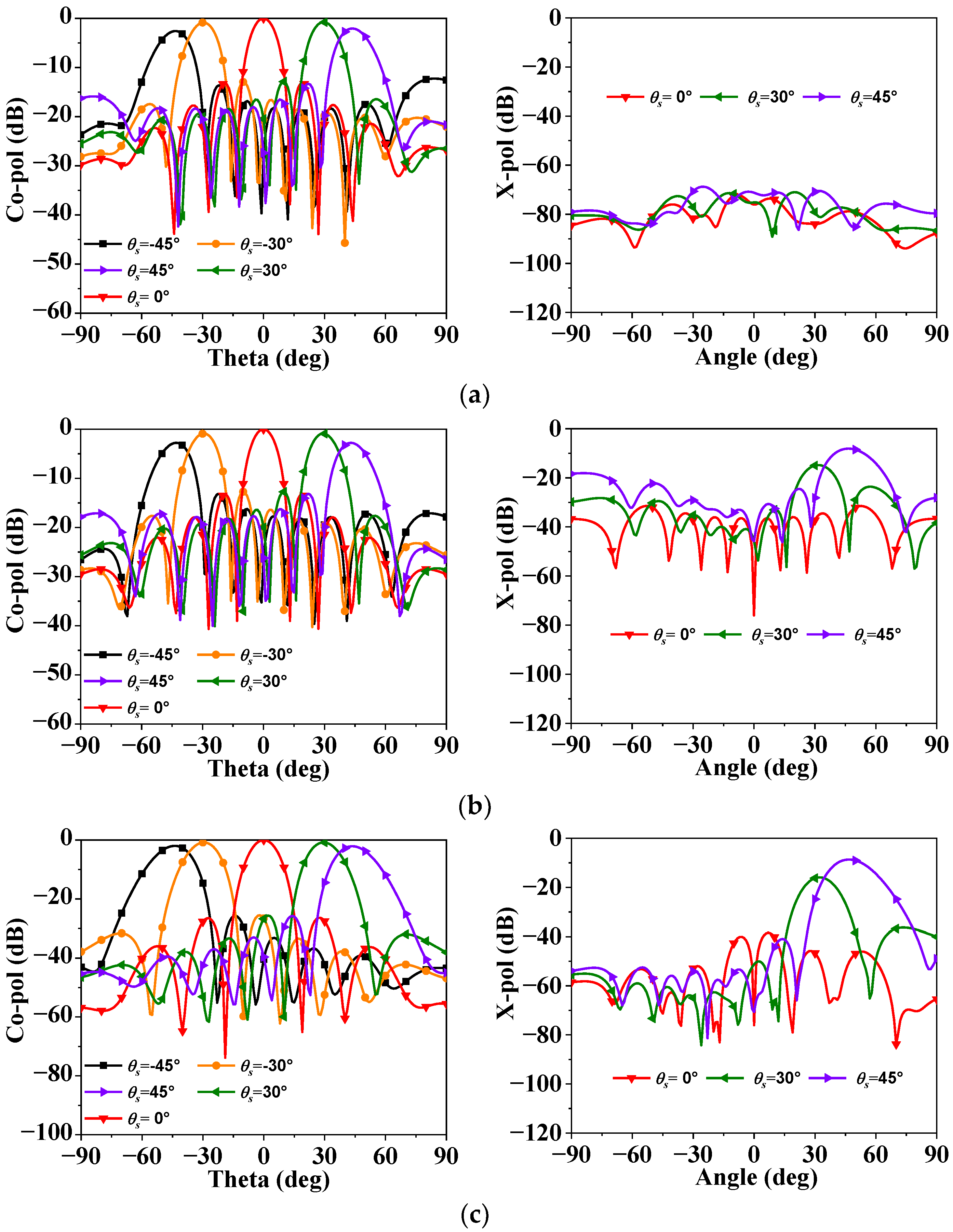
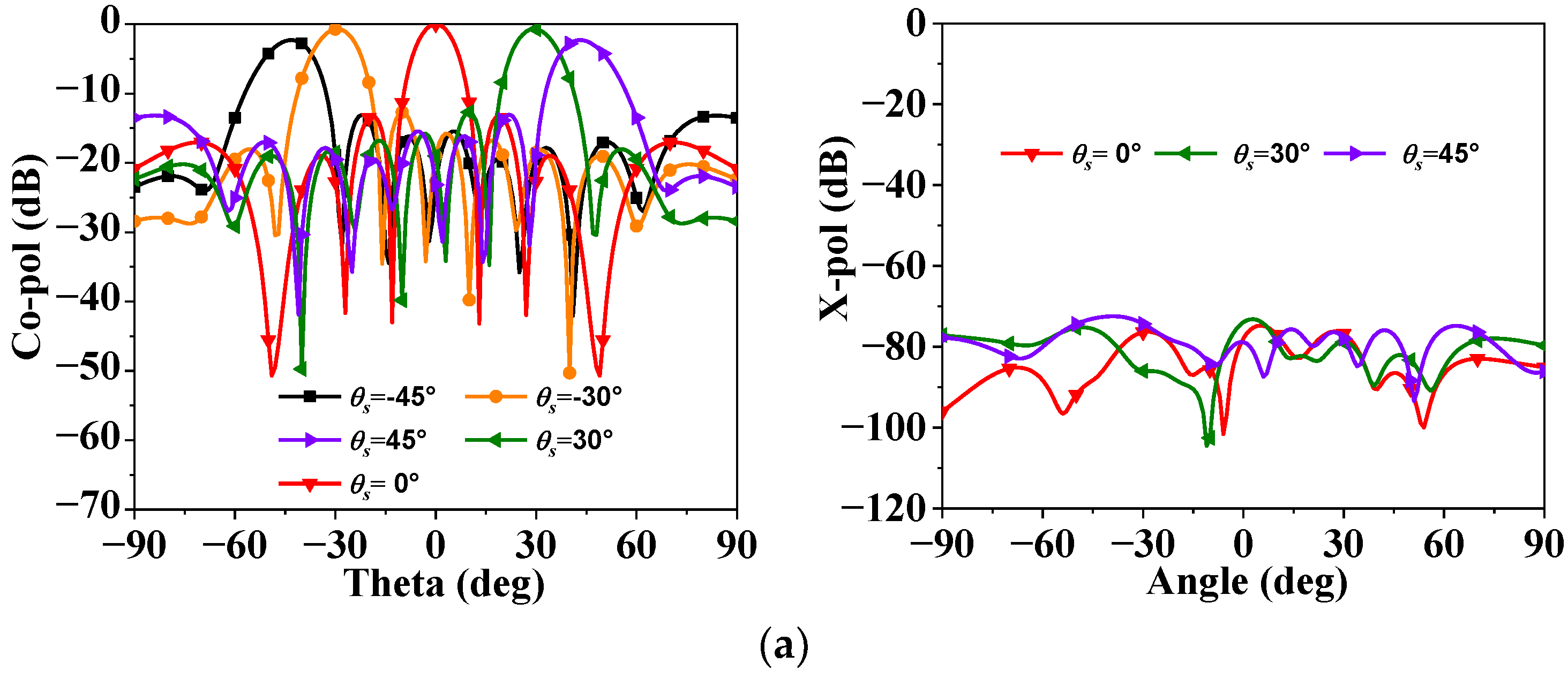
3. Infinite Array Performance

The total size of the antenna is about 0.53λ0 × 0.53λ0, which enables the PAA to provide a wide-angle scan from −45° to 45° without grating lobes theoretically. Figure 4 shows the simulated active VSWRs under broadside and scanned status in E-, H-, and D-planes (diagonal plane) in an infinite array environment. Under the criterion of active VSWR ≤ 3, it can be seen that the Ant-1 array can scan up to ±45° at broadside with a 15.7% bandwidth, and it was approximately 7.6% with a two-dimensional scanning range of ±45°. Due to the feeding asymmetry, the array exhibits a blind spot. With the help of the modified SIW, scan blindness has been shifted from 1.06f0 in Ant-1 to 1.09f0 in Ant-2, far away from the operating band. The bandwidth of Ant-2 array is approximately 7.5% with VSWR ≤ 2.6 when the pattern steers up to ±45° in all planes. The SIW cavity led to a good wide-scanning performance because it can act as a wide-angle impedance matching layer [25,26].

4. Methods for Improving Scanning Performance

Based on the two CBPAs, an 8 × 8 PAA model with 16 four-element subarrays was constructed for comparison with the 2 × 2-element subarray, as depicted in Figure 5. Array 1 consists of the Ant-1 unit, while Array 2 comprises the Ant-2 unit. As mentioned previously, Array 3 is composed of Ant-2 unit, which has undergone sequential rotation. As we know, sequential rotation is often used in designing circular polarized antennas with element angular orientation and feed phase arranged in a 0°, 90°, 0°, 90° fashion or 0°, 90°, 180°, 270° fashion. In this paper, the Array 3 has its elements arranged in 2 × 2 square grid configurations with element angular orientation and feed phase arranged in a 0°, 180°, 180°, 0° fashion. As shown in Figure 4, Array 3 becomes the image arrangement, so it can be said that image arrangement can be called a special case of sequential rotation [27,28].
The mechanism of the 2 × 2-element subarray can also be explained theoretically. From Figure 4, the far-field patterns in the two principal planes, the X-Z plane or the Y-Z plane, can be obtained via a direct summation of the fields from all four patches. We let the total far field in the X-Z plane be denoted by Fxz, the vertical field vector from patch 1 by H1, the vertical field vector from patch 2 by H2, etc. The total far field can then be written as follows:
F y z = H 1 e j k 0 d sin θ e j 0 ° + H 2 e j k 0 d sin θ e j 180 ° + H 3 e j k 0 d sin θ e j 180 ° + H 4 e j k 0 d sin θ e j 0 ° = ( H 1 e j 0 ° + H 4 e j 0 ° ) e j k 0 d sin θ + ( H 2 e j 180 ° + H 3 e j 180 ° ) e j k 0 d sin θ
Since this is a uniformly excited array, H1 = H2 = H3 = H4 = H; therefore
F y z = 2 H e j 0 ° e j k 0 d sin θ + e j 180 ° e j k 0 d sin θ = j 4 H sin ( k 0 d sin θ )
where k0 is the free-space propagation constant, d is the interelement spacing, and θ is the scanning angle.
The H terms represent a pure linearly polarized wave, and the sine term is an element array factor. This total field Fyz is, thus, equivalent to that generated from four linearly polarized elements. In this fashion, the cross-pol level of the array can decrease substantially. This phenomenon can be explained in Figure 5. The solid arrows are edge field due to fundamental TM10 mode, which generates the co-pol radiation. The dashed arrows are edge field due to TM02 mode, which is shown here only as an example and is one of the many modes that contribute to cross-pol. It demonstrates that only the co-pols are reinforced but the cross-pols canceled. It is this cancellation of the cross-pols that permits the low cross-pol in H-plane.
The active element patterns of center element are presented in Figure 6. The observed asymmetry in E-plane is a direct consequence of the strong coupling that exists between the surface waves and the currents present on adjacent planes. This coupling is primarily attributed to the physical discontinuities caused by the probe feed structure [24]. The blind spot has been shifted from 60° in Ant-1 to over 70° in Ant-2. The zeros in the pattern align perfectly with the blind spots identified in the active VSWR. When compared with the radiation pattern of Ant-1, Ant-2 exhibits a broadened beamwidth. Figure 7 depicts the simulated surface current distribution of the radiating patch at fh and serves to elucidate the operational mechanism of the wide-beam antenna. The maximum current amplitude is observed at both the left and right edges of the patch. In contrast to the surface current of Ant-1, Ant-2 displays a more concentrated distribution, which can be regarded as a reduction in the equivalent radiation aperture of the antenna. Consequently, according to antenna theory, this results in a broadened beamwidth.
The phased array factor (AF) at any observation angle (θ, φ) when the PAA is scanned to angle (θs, φs) is given by
A F ( θ , φ ) =   n = 1 N x m = 1 N y I n , m e j ( k sin θ ( n d x cos φ + m d y sin φ ) + ϕ n , m )
where k is the free-space propagation constant, and ϕ n , m is a phase shift equal to the rotation angle. I n , m = e j φ n , m is the excitation applied to the nth and mth elements, n is the antenna column number (n = 0~8), m is the antenna row number (m = 0~8), and φn,m are the phases applied by
φ n , m = k sin ( θ s ) ( n d x cos φ s + m d y sin φ s )
The normalized simulated scanning patterns of different types of PAA in the E-, H- and D-planes at fh (1.03 f0) are illustrated in Figure 8, Figure 9 and Figure 10, respectively. The cross-pol (X-pol) in each case is normalized to its corresponding co-pol. The cross-pol is calculated using Ludwig’s third definition [29]. Array 1 exhibits a gain fluctuation of 3.8 dB in E-plane and 2.6 dB in H-plane with a scanning coverage of 45°. After using the modify SIW cavity, Array 2 demonstrates the ability to scan to ±45° with gain fluctuations of 2.1 dB and 2.6 dB in the E- and H-plane, respectively. Array 3 exhibits a roll-off with a 2.2 dB drop at E-plane and 2.1 dB drop at H-plane at ±45°. Notably, the cross-pol levels are less than −64 dB when scanning ±45° in E-plane. For both Array 1 and Array 2, the cross-pol levels are about −10 dB when patterns are steered to 45° in H-plane. However, after applying SQR, the normalized cross-pol levels of Array 3 are less than −60 dB when patterns are steered to 45° in H-plane. The sidelobe level (SLL) is close to −13.3 dB at broadside. Unfortunately, due to the element pattern and the mismatch of the ports, the SLL gradually increases with the steering angle. The worst simulated SLLs of Array 3 are −10.8 dB and −10.5 dB when scanning over all scan angles in E- and H-planes, respectively. As can be seen from the three figures, the cross-pol levels in the D-plane of the three arrays are almost same, so SQT cannot reduce the cross-polarization level on the D-plane.
Table 1 summarizes the pattern feature of the three PAAs. The peak gains of both Array 1 and Array 2 are 23.7 dBi, but they scanning radiation pattern is asymmetry, which bring different gain fluctuation when scanning the same angle in positive and negative in E-plane. This is mainly due to the embedded element pattern. The X-pol level of is relatively high. The X-pol levels of Array 1 and Array 2 in H-plane is −5.3 dB, and −8.9 dB, respectively. Although the peak gain of Array 3 is 23.6 dB, Array 3 has a symmetry scanning radiation pattern. Moreover, Array 3 exhibits low gain fluctuation of less than 2.3 dB. The X-pol levels of Array 3 are less than −74.5 dB in E- and H-planes. Comparing these results, the scanning potential of proposed SIW patch array is significantly better. It should be noted that the proposed results are not optimal, it is just a demo case.
It is worth mentioning that the PAA could not be exactly steered to 45°, though each port is an ideal feed with the intended beam scanning angle, owing to the finite array aperture. According to our simulated results in an 8 × 8 array, for these radiation patterns in the E- and H-Planes, the main lobe can be exactly steered at 29° when scanning to 30°. Nevertheless, even if each port of the unit is fed with theoretical phase for scan angles of 45°, the main lobe will steer to 43°. If the finite array aperture is large enough, such as an array with 64 × 64 elements, the beam pointing will be completely consistent with the theory.

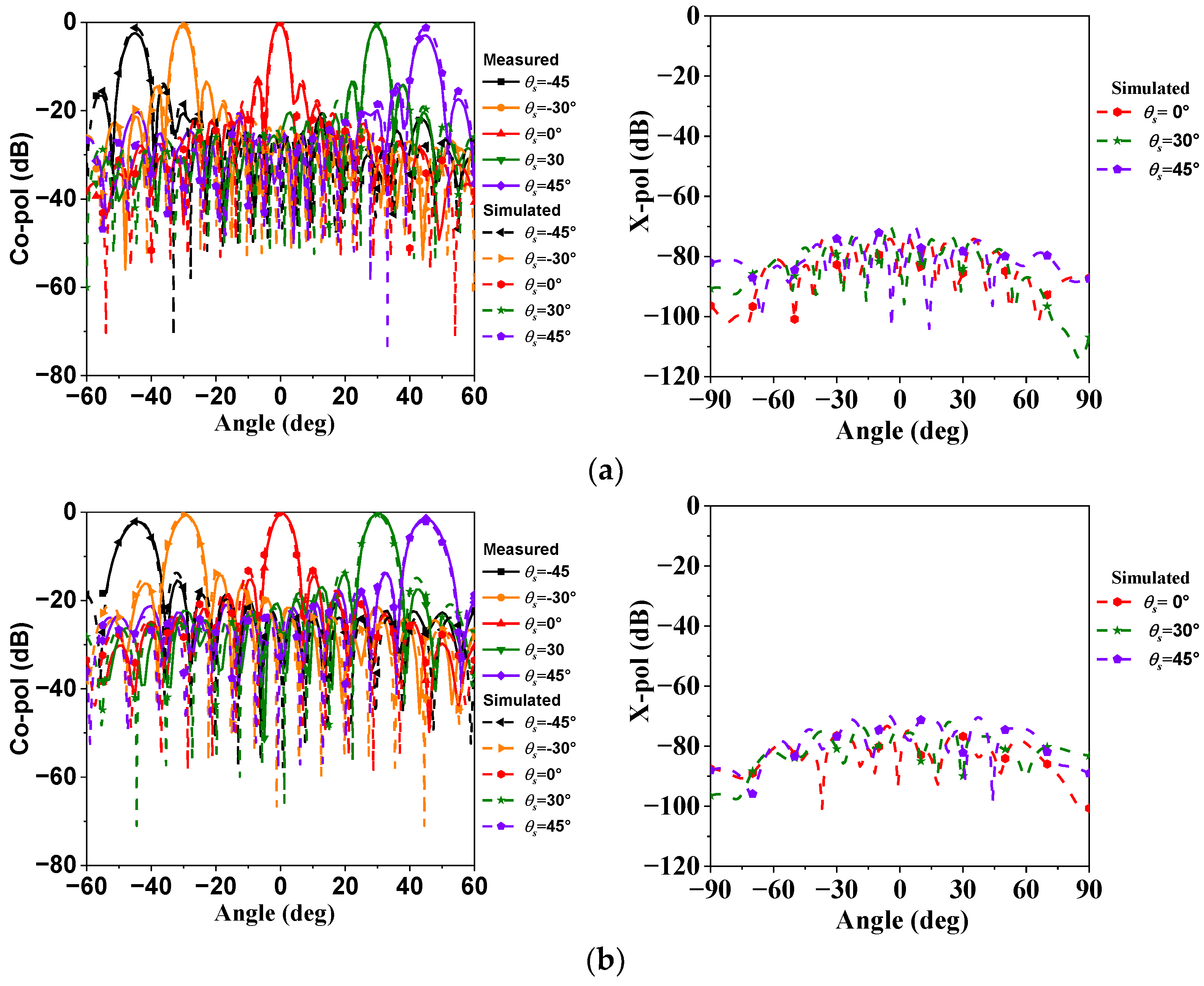
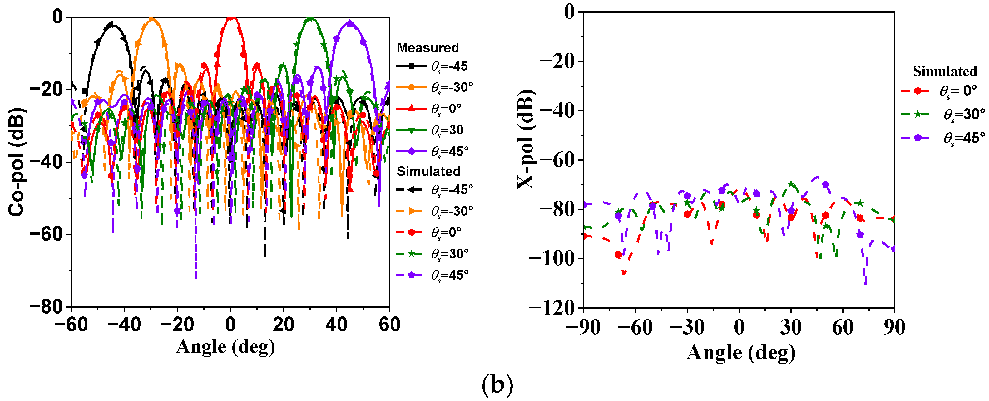
5. Finite Array Experimental Results

To meet the requirements for radar system, a 24 × 16 (384-element) PAA of Array 3 was simulated, fabricated, and measured, as depicted in Figure 11a. Due to confidentiality requirements, the center operating frequency is replaced by fo. As the fabricated array is a 24 × 16 (384-element) array, the overall size of the array is 12.72 λ0 × 8.48 λ0. The proposed array structure is a double-layer microwave board, which is manufactured on the basis of conventional PCB technology. The microwave board is welded onto the support metal plate via the tin–lead solder process after the subminiature version P (SMP) connectors have been soldered on it. Most notably, the SMP connector is the optimization choice for antenna at the Ku band. Uniform amplitude distribution is used in the PAA aperture. The 384-element PAA is tested using an active T/R module. The calibration of the 384-element PPA was initially conducted successfully using the method in [30] with a near-field antenna probe across the operating frequency range. However, only phase calibration was carried out for the phased array. Figure 11b shows the PAA during performance characterization measurements in the anechoic chamber. Since the active PAA only tests EIRP, the gain is not measured separately.
Figure 12 plots the simulated realized peak gains and efficiency of proposed 384-unit PAA. The theoretical aperture gain is calculated using 4πS/λ02, where S is the aperture area of PAA, and λ0 is the wavelength of operating frequency in free space. The simulated gain is higher than 31 dBi at broadside and higher than 28.4 dBi when steering up to ±45°. The simulated efficiency is higher than 85% at broadside in the operating bandwidth. We can see that the array gain gradually increases with frequency and decreases with scanning angle.
Figure 13, Figure 14 and Figure 15 present the measured and simulated scanning performances at fl, f0, and fh in E- and H-planes. The scanning angles of the presented array are 0°, ±30°, and ±45° in the two orthogonal principal planes. The cross-pol levels in E- and H-planes were too low to be measured, and only simulated cross-polarization was provided. It can be seen that the proposed 24 × 16 array showed the ability to scan up to ±45° in E- and H-planes without grating lobes.
At fl, the proposed PAA exhibits gain fluctuations of 1.2 dB and 2.1 dB in E- and H-planes, respectively, with a scanning coverage of 45°. It can be seen that when scanning to 45°, the simulated normalized cross-pol levels are around −86.5 dB in E- and H-planes. The simulated SLLs are −12.6 dB and −11.6 dB when scanning over all scan angles in E- and H-planes, respectively. At f0, the proposed PAA shows the ability to scan to ±45° with gain fluctuations of 1.5 dB and 1.9 dB in E- and H-plane, respectively. It can be seen that when patterns are steered to 45°, the simulated normalized cross-pol levels are less than −68 dB, both in E- and H-planes. The simulated SLLs are −12 dB and −11.7 dB in E- and H-plane, respectively. At fh, the proposed PAA exhibits a roll-off with 2 dB and 2.14 dB drops in E-plane and H-plane at ±45°. It can be seen that when scanning over all scan angles, the simulated normalized cross-pol levels are closed to −82.7 dB in E- and H-planes. The simulated SLLs are −12.3 dB and −11.6 dB when scanning over all scan angles in E- and H-planes, respectively.
Remarkably, the measured results show that the proposed PAA can steer to ±45° with impressive gain fluctuations of 2.2 dB and 2.9 dB in E-plane and H-plane, respectively. We note that the cross-polarization level is less than −68 dB during the scanning in the two principal planes. The SLL is less than −11.6 dB within the scanning range of ±45° in the two main planes over the operation frequency band. Better SLLs can be acquired by employing the appropriate amplitude weighting. In general, the measured and simulated results agree well, including sidelobe levels and beamwidth, particularly in the main beam direction. It is noteworthy that the measured scanning gain fluctuation in the scan range of ±45° surpasses the simulated one. This disparity can be attributed mainly to fabrication, soldering, and assembly tolerances. Table 2 shows the detailed simulated/measured scanning loss when scanning to ±45°.
Table 3 summarizes the performance of the proposed phased array. A comparison with other previous state-of-the-art phased arrays is also shown. In [15], the array is capable of 2D scanning with a roll-off with 3 dB, but the -pol level is relatively high in H-plane because it is a conventional array, even if it does not provide the X-pol level. Although the PAA in [16] exhibits a low gain fluctuation of 0.5 dB in E-plane, the scan range is only 15°, and the X-pol level is only −14 dB in H-plane. Though the PAA in [21] has a wide-angle scanning performance with low roll-off at 60° with small element space, the proposed design is able to have a low cross-polarization level in all planes rather than one plane. Moreover, it has a low gain fluctuation at 45° with 0.53λ0 element space. Thus, among the tabulated antennas outlined above, the proposed PAA has the most outstanding X-pol level, especially in H-plane. Furthermore, the proposed PAA exhibits a low gain fluctuation. Therefore, the proposed PAA has huge potential to be implemented in radar systems.

6. Conclusions

In this paper, an effective method is developed to improve the scanning performances of PAAs. Both modified SIW cavities and SQTs were used. The proposed array-simulated results achieve excellent scanning performance with 2.2 dB gain fluctuation and better than −68.1 dB cross-polarization levels both in the E- and H-plane when scanning up to ±45° over the whole working band. Moreover, the proposed PAA achieved symmetric scanning pattern in E-plane. Without any parasitic structure, the array has the advantages of low cost and a simple structure. A 24 × 16 array was simulated, fabricated, and measured. The measured scanning radiation patterns demonstrated good agreement with the simulated results. As a result, the presented array is a good candidate for high-performance PAA applications with fixed dimensions. Although it has a wide range of applications and enormous potential, more research and development are required. For example, as proof-of-concept, this study only shifted the blind spot and had a narrow operating bandwidth. Therefore, future research will focus on how to improve the array performance by eliminating blind spots.

Author Contributions

Conceptualization, A.Q. and X.L.; methodology, H.L.; software, T.G.; validation, C.F. and S.Z.; formal analysis, H.L. and X.X.; investigation, T.G.; resources, C.F. and S.Z.; data curation, Z.X.; writing—original draft preparation, H.L. and T.G.; writing—review and editing, H.L. and A.Q.; supervision, A.Q., and X.L.; project administration, X.L.; funding acquisition, H.L., X.X., and X.L. All authors have read and agreed to the published version of the manuscript.

Funding

This work was supported in part by the Key Research and Development Program of Zhejiang Province under Grant No. 2022C01093, in part by National Natural Science Foundation of China under Grant No. 62271122, in part by Huzhou Municipal Natural Science Foundation of China under Grant Nos. 2023YZ19, and in part by Scientific Research Foundation for Yangtze Delta Region Institute of University of Electronic Science and Technology of China, Huzhou, under Grant No. U03220083.

Data Availability Statement

The data that support the findings of this study are available from the corresponding author upon reasonable request.

Conflicts of Interest

The authors declare no conflicts of interest.

References

  1. Hu, C.; Wang, B.; Gao, G.; Wang, R.; Xiao, S.; Ding, X. Conjugate Impedance Matching Method for Wideband and Wide-Angle Impedance Matching Layer With 70° Scanning in the H-Plane. IEEE Antennas Wirel. Propag. Lett. 2021, 20, 63–67. [Google Scholar] [CrossRef]
  2. Zeng, Q.; Chen, Z.; He, M.; Wang, S.; Liu, X.; Xu, H. Design of a Ka-Band Heterogeneous Integrated T/R Module of Phased Array Antenna. Electronics 2024, 13, 204. [Google Scholar] [CrossRef]
  3. Hu, C.; Wang, B.; Wang, R.; Xiao, S.; Ding, X. Ultrawideband, Wide-Angle Scanning Array with Compact, Single-Layer Feeding Network. IEEE Trans. Antennas Propag. 2020, 68, 2788–2796. [Google Scholar] [CrossRef]
  4. Yang, G.; Li, J.; Wei, D.; Xu, R. Study on Wide-Angle Scanning Linear Phased Array Antenna. IEEE Trans. Antennas Propag. 2018, 66, 450–455. [Google Scholar] [CrossRef]
  5. Xu, Z.; Zhang, C.; Kaufmann, T.; Yan, X.; Yuan, Y.; Fumeaux, C. Analysis of Scan Blindness in a Linearly Polarized Tapered-Slot Phased Array in Triangular Lattice—Performance Improvement with Parasitic Notches. IEEE Trans. Antennas Propag. 2014, 62, 4057–4066. [Google Scholar] [CrossRef]
  6. Jin, F.; Ding, X.; Cheng, Y.; Wang, B.; Shao, W. A Wideband Phased Array with Broad Scanning Range and Wide-Angle Impedance Matching. IEEE Trans. Antennas Propag. 2020, 68, 6022–6031. [Google Scholar] [CrossRef]
  7. Jin, F.; Ding, X.; Cheng, Y.; Wang, B.; Shao, W. Impedance Matching Design of a Low-Profile Wide-Angle Scanning Phased Array. IEEE Trans. Antennas Propag. 2019, 67, 6401–6409. [Google Scholar] [CrossRef]
  8. Sun, D.; Hao, Z.; Ding, C.; Liu, R.; Guo, Z.; Yin, H. A Low-Profile Ultra-Wideband and Wide-Scanning Phased Array for UHF Applications. IEEE Trans. Antennas Propag. 2023, 71, 473–486. [Google Scholar] [CrossRef]
  9. Bermúdez-Martín, D.; Gillard, R.; Molero, C.; Legay, H.; García-Vigueras, M. Methodology for Improving Scanning Performance Loading an Array Element with a 3D All-Metal WAIM. Electronics 2022, 11, 2848. [Google Scholar] [CrossRef]
  10. Vilenskiy, A.; Litun, V.; Lyulyukin, K. Wideband Beam Steering Antenna Array of Printed Cavity-Backed Elements With Integrated EBG Structure. IEEE Antennas Wirel. Propag. Lett. 2019, 18, 245–249. [Google Scholar] [CrossRef]
  11. Kiani-Kharaji, M.; Hassani, H.; Mohammad-Ali-Nezhad, S. Wide scan phased array patch antenna with mutual coupling reduction. IET Microw. Antennas Propag. 2018, 12, 1932–1938. [Google Scholar] [CrossRef]
  12. Yang, G.; Li, J.; Xu, R.; Ma, Y.; Qi, Y. Improving the Performance of Wide-Angle Scanning Array Antenna with a High-Impedance Periodic Structure. IEEE Antennas Wirel. Propag. Lett. 2016, 15, 1819–1822. [Google Scholar] [CrossRef]
  13. Sun, B.; Ding, X.; Cheng, Y.; Shao, W. 2-D Wide-Angle Scanning Phased Array with Hybrid Patch Mode Technique. IEEE Antennas Wirel. Propag. Lett. 2020, 19, 700–704. [Google Scholar] [CrossRef]
  14. Wang, Y.; Ding, X.; Zhang, L.; Shao, W.; Wang, B. A Low-Cost Wideband Dual Circularly Polarized Aperiodic 2-D Phased Array. IEEE Trans. Antennas Propag. 2023, 71, 3080–3090. [Google Scholar] [CrossRef]
  15. Guo, J.; Hu, Y.; Hong, W. A 45° Polarized Wideband and Wide-Coverage Patch Antenna Array for Millimeter-Wave Communication. IEEE Trans. Antennas Propag. 2022, 70, 1919–1930. [Google Scholar] [CrossRef]
  16. Liu, H.; Qing, A.; Xu, Z.; Yu, Z.; Zhang, S. Design of Physically Connected Wideband SIW Cavity-Backed Patch Antenna for Wide-Angle Scanning Phased Arrays. IEEE Antennas Wirel. Propag. Lett. 2021, 20, 406–410. [Google Scholar] [CrossRef]
  17. Cheng, Y.; Ding, X.; Shao, W.; Wang, B. Planar Wide-Angle Scanning Phased Array with Pattern-Reconfigurable Windmill-Shaped Loop Elements. IEEE Trans. Antennas Propag. 2017, 65, 932–936. [Google Scholar] [CrossRef]
  18. Xia, R.; Qu, S.; Li, P.; Yang, D.; Yang, S.; Nie, Z. Wide-Angle Scanning Phased Array Using an Efficient Decoupling Network. IEEE Trans. Antennas Propag. 2015, 63, 5161–5165. [Google Scholar] [CrossRef]
  19. Xia, R.L.; Qu, S.W.; Yang, S.; Chen, Y. Wideband Wide-Scanning Phased Array with Connected Backed Cavities and Parasitic Striplines. IEEE Trans. Antennas Propag. 2018, 66, 1767–1775. [Google Scholar] [CrossRef]
  20. Rodríguez Ulibarri, P.; Crépin, T.; Martel, C.; Boust, F.; Falcone Lanas, F.J.; Loecker, C.; Herbertz, K.; Bertuch, T.; Dousset, T.; Martinaud, J.P.; et al. Experimental demonstration of metamaterials application for mitigating scan blindness in phased array antennas. EPJ Appl. Metamaterials 2016, 3, 9. [Google Scholar] [CrossRef]
  21. Aljuhani, A.; Kanar, T.; Zihir, S.; Rebeiz, G. A 256-Element Ku-Band Polarization Agile SATCOM Receive Phased Array with Wide-Angle Scanning and High Polarization Purity. IEEE Trans. Microw. Theory Tech. 2021, 69, 2609–2628. [Google Scholar] [CrossRef]
  22. Aljuhani, A.; Kanar, T.; Zihir, S.; Rebeiz, G. A 256-Element Ku-Band Polarization Agile SATCOM Transmit Phased Array with Wide-Scan Angles, Low Cross Polarization, Deep Nulls, and 36.5-dBW EIRP per Polarization. IEEE Trans. Microw. Theory Tech. 2021, 69, 2594–2608. [Google Scholar] [CrossRef]
  23. Low, K.; Zihir; Kanar, T.; Rebeiz, G. A 27–31-GHz 1024-Element Ka-Band SATCOM Phased-Array Transmitter With 49.5-dBW Peak EIRP, 1-dB AR, and ±70° Beam Scanning. IEEE Trans. Microw. Theory Tech. 2022, 70, 1757–1768. [Google Scholar] [CrossRef]
  24. Banerjee, R.; Sharma, S.K.; Waldstein, S.W.; Downey, J.M.; Schoenholz, B.L.; Dever, S.M.; Nessel, J.A.; Das, S. A 22-28 GHz Polarization-Reconfigurable Flat-Panel 8 × 8 Tx/Rx Phased Array Antenna with Uniquely Arranged Novel Radiating Elements for CubeSat Communication. IEEE Trans. Antennas Propag. 2023, 73, 4138–4152. [Google Scholar] [CrossRef]
  25. Awida, M.; Kamel, A.; Fathy, A. Analysis And Design of Wide-Scan Angle Wide-Band Phased Arrays of Substrate-Integrated Cavity-Backed Patches. IEEE Trans. Antennas Propag. 2013, 61, 3034–3041. [Google Scholar] [CrossRef]
  26. Valavan, S.; Tran, D.; Yarovoy, A.; Roederer, A. Planar Dual-Band Wide-Scan Phased Array in X-Band. IEEE Trans. Antennas Propag. 2014, 62, 5370–5375. [Google Scholar] [CrossRef]
  27. Ortiz, J.A.; Salazar-Cerreno, J.L.; Díaz, J.D.; Lebrón, R.M.; Aboserwal, N.A.; Jeon, L. Low-cost CMOS Active Array Solution for Highly Dense X-Band Weather Radar Network. IEEE Trans. Antennas Propag. 2020, 68, 5421–5430. [Google Scholar] [CrossRef]
  28. Saeidi-Manesh, H.; Zhang, G. Challenges and Limitations of The Cross-Polarization Suppression in Dual-Polarization Antenna Arrays Using Identical Subarrays. IEEE Trans. Antennas Propag. 2020, 68, 2853–2866. [Google Scholar] [CrossRef]
  29. Ludwig, A. The definition of cross polarization. IEEE Trans. Antennas Propag. 1973, 21, 116–119. [Google Scholar] [CrossRef]
  30. Hampson, G.; Smolders, A. A Fast and Accurate Scheme for Calibration of Active Phased-Array Antennas. In Proceedings of the IEEE Antennas and Propagation Society International Symposium. 1999 Digest. Held in conjunction with: USNC/URSI National Radio Science Meeting (Cat. No.99CH37010), Orlando, FL, USA, 11–16 July 1999; Volume 2, pp. 1040–1043. [Google Scholar]
Figure 1. Evolution diagram of the proposed antenna element.
Electronics 13 01776 g001
Figure 2. Exploded view of the proposed antenna element.
Electronics 13 01776 g002
Figure 3. Simulated |S11| of antennas 1 and 2.
Electronics 13 01776 g003
Figure 4. Simulated active VSWR in an infinite array.
Electronics 13 01776 g004
Figure 5. Four-element (2 × 2) subarrays of different types.
Electronics 13 01776 g005
Figure 6. Comparison of the simulated patterns of the central element at fh.
Electronics 13 01776 g006
Figure 7. Simulated current distributions of the center element.
Electronics 13 01776 g007
Figure 8. Normalized patterns of Array 1 at fh: (a) E-plane, (b) H-plane, and (c) D-plane.
Electronics 13 01776 g008
Figure 9. Normalized patterns of Array 2 at fh: (a) E-plane, (b) H-plane, and (c) D-plane.
Electronics 13 01776 g009
Figure 10. Normalized patterns of Array 3 at fh: (a) E-plane, (b) H-plane, and (c) D-plane.
Electronics 13 01776 g010aElectronics 13 01776 g010b
Figure 11. Fabricated prototype: (a) photograph of the fabricated 24 × 16 prototype; (b) pattern measurement setup.
Electronics 13 01776 g011
Figure 12. Simulated current distributions of the center element.
Electronics 13 01776 g012
Figure 13. Normalized patterns at fl: (a) E-plane and (b) H-plane.
Electronics 13 01776 g013
Figure 14. Normalized patterns at f0: (a) E-plane and (b) H-plane.
Electronics 13 01776 g014aElectronics 13 01776 g014b
Figure 15. Normalized patterns at fh: (a) E-plane and (b) H-plane.
Electronics 13 01776 g015
Table 1. Comparison of the three PAAs.
WorkPeak Gain/dBiScan Loss/dB
(45°/−45°)
Blind Spot X-Pol Level/dB
(45°/−45°)
Pattern
Array 123.7E: 2.3/3.8
H: 3.3/3.3
@1.06f0E: −66.2
H: −5.32
Asymmetry
Array 223.7E: 2.1/2.6
H: 2.3/2.8
@1.09f0E: −73.1
H: −8.97
Asymmetry
Array 323.6E: 2.3/2.3
H: 2.1/2.1
@1.09f0E: −75.5
H: −74.5
Symmetry
Table 2. Simulated/measured scanning loss.
SimulatedMeasured
FrequencyE-PlaneH-PlaneE-PlaneH-Plane
fl1.23 dB @±45°2.06 dB @±45°2.9 dB @±45°2.14 dB @±45°
f01.45 dB @±45°1.92 dB @±45°2.9 dB @±45°2.9 dB @±45°
fh1.98 dB @±45°1.8 dB @±45°3.8 dB @±45°3.7 dB @±45°
Table 3. A comparison with the state-of-the-art proposed PAA.
WorkGain Fluctuation-Pol Level/dB
(45°/−45°)
ApproachesPattern
[15]E: 3dB @±45°
H: 3 dB @±45°
-SIW cavitySymmetry
[16]E: 0.5dB @±15°
H: 3 dB @±45°
E: −64 dB @45°
H: −14 dB @45°
SIW cavityAsymmetry
[21]E: 4.1 dB @±60°
H: 5.2 dB @±60°
E: −29 dB @60°
H: −23 dB @60°
SQTSymmetry
This workE: 2.9 dB @±45°
H: 2.2 dB @±45°
E: −72.3 dB @45°
H: −68.1 dB @45°
SQT and SIW cavitySymmetry
Disclaimer/Publisher’s Note: The statements, opinions and data contained in all publications are solely those of the individual author(s) and contributor(s) and not of MDPI and/or the editor(s). MDPI and/or the editor(s) disclaim responsibility for any injury to people or property resulting from any ideas, methods, instructions or products referred to in the content.

