
Study on Radiation Damage of Silicon Solar Cell Electrical Parameters by Nanosecond Pulse Laser

State Key Laboratory of Laser Propulsion & Application, Space Engineering University, Beijing 101400, China
*
Authors to whom correspondence should be addressed.
Electronics 2024, 13(9), 1795; https://doi.org/10.3390/electronics13091795
Submission received: 12 April 2024
/
Revised: 29 April 2024
/
Accepted: 1 May 2024
/
Published: 6 May 2024
(This article belongs to the Special Issue Radiation Effects of Advanced Electronic Devices and Circuits, 2nd Edition)
Abstract
:This experimental study investigates the damage effects of nanosecond pulse laser irradiation on silicon solar cells. It encompasses the analysis of transient pulse signal waveform characteristics at the cells’ output and changes in electrical parameters, such as I–V curves before and after laser irradiation under varying laser fluence and background light intensities, and explores the underlying action mechanisms of laser irradiation. The study reveals that as the laser fluence increases up to 4.0 J/cm2, the peak value of the transient pulse signal increases by 47.5%, while the pulse width augments by 88.2% compared to the initial transient pulse signal. Furthermore, certain parameters, such as open-circuit voltage, short-circuit current, and peak power obtained, from the measured I–V curve indicate a threshold laser fluence for functional degradation of the solar cell at approximately 1.18 ± 0.42 J/cm2. Results obtained from laser irradiation under different background light intensities underscore the significant influence of background light on laser irradiation of silicon cells, with the most severe damage occurring in the absence of light. Moreover, findings from laser irradiation at multiple locations on the silicon cell demonstrate a linear decrease in the output voltage of the silicon cell with an increase in the number of irradiation points.
1. Introduction
A laser beam has significant advantages, such as high directionality and monochromaticity, good coherence, and high brightness. It has been widely used in materials (including metal and non-metal) cutting, surface treatment, perforation, and micro-machining, among other applications. Solar cells are photoelectric conversion devices that directly convert light into electrical energy without an external power source. As a photosensitive device, solar cells are susceptible to damage from laser irradiation, resulting in reduced photoelectric conversion efficiency, structural damage, and functional total or partial loss. Increasing the power of incident light on solar cells enhances the output, but high-power monochromatic light irradiation may cause severe damage to them. Currently, the most widely used silicon solar cells present a high absorption rate and a low reflectivity for a 1.1 μm laser, but their photoelectric conversion efficiency is generally between 10% and 20%. Therefore, a significant part of the incident laser beam energy converts into thermal energy that heats and damages the solar cell. When the incident laser beam energy is much greater than the energy that the solar cell can absorb, the incident laser beam will increase the temperature of the cell, leading to a significant decrease in efficiency. The research on laser irradiation of solar cells began with the concept of laser wireless power transmission. Glaser proposed the idea of establishing a solar power collection system in space to transmit abundant solar energy to ground-based solar cells through laser transmission. The American Explorer detector discovered that high-energy charged particle radiation in space can cause damage to the performance of solar cells. With the further development and application of laser technology, attention has gradually focused on researching the damage and protection of laser-irradiated solar cells.
In 1973, Matsuoka and Usami first conducted a series of studies on the laser irradiation of solar cells. The experiments found that excessive power of pulsed lasers leads to a decrease in the peak power of solar cells [1,2,3]. Recently, research has been conducted on the irradiation damage of solar cells using continuous laser [4,5,6,7,8,9] and pulsed laser [10,11,12], accounting for the effects of different wavelengths [13,14,15], employing different pulse widths [16,17], and varying the laser parameters, such as laser fluence and frequency [18,19,20,21,22]. The damage effect of laser irradiation on silicon materials used in solar cells and its mechanism have been the focus of research [23,24,25]. The investigation of the damage to silicon materials mainly focuses on the damage caused by heat and stress. However, this does not directly reflect the electrical damage of silicon-based electronic devices. Most of the research on laser-irradiated solar cells treats the damage threshold, temperature response, stress damage, and damage morphology of solar cells under different laser parameters or irradiation modes. Photosensitive devices, such as silicon-based photodiodes [26,27], present significant transient electrical signals under laser irradiation. These transient signals are the direct response of the device to the laser, and their characteristics can indicate the interaction process between the laser and the device. Analogously, solar cells can generate photoelectric signals even under weak laser conditions. These signals are crucial for analyzing the intrinsic mechanism of weak laser-induced damage to solar cells. However, the characteristics of these laser-induced transient pulse signals have not received much attention.
In this study, we developed an acquisition circuit to detect the transient pulse signal resulting from laser irradiation on silicon cells. We conducted experiments to investigate the characteristics of the transient pulse signal under different laser fluences, varying background light intensities, and multi-point irradiation scenarios on the same cell. Simultaneously, we obtained the I–V curve of the cell under different experimental conditions and analyzed the underlying mechanism of laser action. The photoelectric signal extraction method employed in this research is innovative, and the findings can offer valuable insights for implementing damage protection measures for solar cells to resistant lasers.
2. Device and Methods
2.1. Device and Signal Acquisition Circuit
The operational mechanism of solar cells is based on the photovoltaic effect of semiconductor materials. This effect describes the generation of charge carriers within semiconductor materials when exposed to light irradiation, and the charge carriers, upon separation, accumulate at the respective ends of a PN junction, thus establishing a potential difference. When an external circuit is connected to both ends of the PN junction, the photocurrent flows through the load. Figure 1 illustrates the operational concept of a silicon solar cell. When the energy of incident photons (hv) surpasses the bandgap width (Eg) of the semiconductor material, numerous electron–hole pairs get excited. If these pairs form within the vicinity of the PN junction’s diffusion length, they can potentially diffuse into the depletion region of the PN junction before undergoing recombination. Under the strong electric field in the depletion region, the electrons migrate toward the N region while holes move toward the P region. This migration leads to a negative charge in the N region and a positive charge in the P region. The electrodes at the sides of the PN junction connect to the load, and the photocurrent flows through the circuit, thus accomplishing power output.
The experimental setup utilized a polycrystalline silicon solar cell measuring 45 mm × 45 mm. The silicon cell exhibits operating voltage, open-circuit voltage, and short-circuit current of 1 V, 1.2 V, and 0.2 A, respectively, with a conversion efficiency of 18%.
Figure 2 depicts the acquisition circuit diagram for the output voltage signal at the load end of the solar cell. R0 is a small resistance, while Rm denotes the optimal matching resistance corresponding to the cell’s highest output power. The resistance calculated according to the measured I–V curve is used as a reference for Rm. For the silicon cell employed in this experiment, the circuit features R0 and Rm values of 0.1 ohms and 4.3 ohms, respectively.
2.2. Methods
The laser employed was a neodymium yttrium aluminum garnet (Nd: YGA) laser with a wavelength of 1064 nm and a pulse width of 10 ns. Figure 3 shows the schematic diagram of the experimental setup. The laser beam section is first shaped by the aperture and then sequentially passes through the attenuator and spectroscope before finally reaching the focusing lens. After being focused by a lens, the laser incidences on the surface of the silicon cell, with a section of Φ = 4 mm. The attenuator adjusts the laser beam intensity, and the spectroscope divides the beam into two paths: one for irradiating the solar cell and the other for laser beam intensity measurement. At the sample location, a Solar-500 xenon lamp (emitting spectra in the range of 200 nm–2500 nm) is used as a solar simulator to provide background light when the Si cell is working. The light intensity of the lamp is adjustable by controlling the current. Throughout the experiment, the voltage probe is connected across the sampling resistor to gather the output voltage of the Si cell and the transient pulse signal produced upon laser irradiation.
This experimental strategy involved conducting laser irradiation experiments with varying laser beam energies, background light intensities, and laser irradiation positions. The experiment involved measuring the voltage–current characteristic curves of the cell both before and after laser irradiation, alongside capturing transient voltage signals generated during the irradiation process. We measured the voltage–current characteristic curve of the cell using a Keithley 2450 instrument. The voltage signals were recorded by the oscilloscope. Electrical parameters of the cell, such as open-circuit voltage, short-circuit current, and peak power, were extracted from the volt–ampere characteristic curve. Subsequently, the analysis focused on the changes in these parameters following laser irradiation.
3. Results
3.1. Results at Different Laser Fluences
Figure 4 shows the transient pulse signals generated at the silicon cell output when irradiated by a single-pulse laser; each curve corresponds to a different laser fluence. The curves show that when the laser fluence is 0.24 J/cm2, the laser does not cause any disturbance to the cell. When the laser fluence is 0.76 J/cm2 or more, it generates a disturbance voltage signal at the output of the Si cell. After the disturbance, the voltage at the output of the cell returns to the level before irradiation. Upon reaching or surpassing 1.6 J/cm2, the disturbance signal increases in duration and peak voltage. Furthermore, following laser irradiation, the cell output voltage fails to recover its pre-irradiation level, suggesting a notable decline in cell performance. We conclude that the interference threshold of laser-irradiated solar cells is 0.76 ± 0.26 J/cm2, and the damage threshold is about 1.18 ± 0.42 J/cm2.
Figure 5a,b show the I–V and P–V curves of the Si cell before and after single-pulse laser irradiation at different laser fluences. Table 1 presents the output voltage of the Si cell, the open-circuit voltage, the short-circuit current, and the peak power extracted from Figure 5. Table 1 indicates that when the laser fluence is less than or equal to 0.76 J/cm2, it does not cause significant damage to the cell’s performance. Increasing the laser fluence from 1.6 J/cm2, the output voltage and peak power of the Si cell show a significant decrease, the open-circuit voltage also decreases, and the short-circuit current does not change considerably.
3.2. Results at Different Background Light Intensities
Figure 6 shows the transient pulse signal generated at the output of the Si cell when irradiated with a single-pulse laser at different background light intensities. The figure indicates that regardless of the background light (corresponding to different initial voltages of the cell), the laser irradiation will cause a larger transient pulse signal at the cell’s output. When there is background light, the amplitudes of the transient pulse signal generated by laser irradiation under 550 W/cm2 and 1100 W/cm2 are almost the same (about 1400 mV). When there is no background light, the amplitude of the transient pulse signal is significantly higher (approximately 1540 mV). Additionally, with the increase in background light intensity, the pulse width of the transient pulse signal gradually widens.
Figure 7a,b show the I–V and P–V curves of the Si cell under single-pulse laser irradiation at different background light intensities. Table 2 indicates the output voltage of the Si cell under laser irradiation, as well as the open-circuit voltage, short-circuit current, and peak power, as extracted from Figure 7. Table 2 indicates that background light is an important influencing factor on the characteristics of silicon cells under laser irradiation. Moreover, the performance of the cells is more severely damaged when there is no light. Coinciding with this observation, it is evident that as the light intensity decreases, the cell’s peak power and open-circuit voltage decline, while the short-circuit current initially remains constant before eventually increasing.
3.3. Results of Multi-Point Irradiation
Figure 8 shows the ablation points generated by laser irradiation on Si cells during the experiments. A total of 6 times of laser irradiation were carried out, and the order of ablation points is shown in the figure.
Figure 9a shows the transient pulse signal generated at the output of the Si cell at different irradiation positions. The figure indicates that each transient pulse signal is similar. The peak values of these transient pulse signals are 1350 mV, 1390 mV, 1370 mV, 1410 mV, 1360 mV, and 1410 mV, successively. Figure 9b depicts the output voltage of the Si cell after each laser irradiation. The Si cell output voltage decreases linearly with an increase in the number of laser irradiation points. After applying six pulse lasers, the Si cell output voltage dropped from 855 mV to 455 mV, which means that the performance of the Si cell decreased by about 47%.
Figure 10a,b depict the I–V and P–V curves of Si cells following laser irradiation at various positions. These figures demonstrate that each laser irradiation induces a degree of performance degradation in the cell.
4. Discussions
4.1. The Influence of Laser Fluence
Figure 11 illustrates the variation in peak voltage and pulse width of the transient voltage signal at the output of the Si cell with increasing laser fluence. The graph reveals three distinct stages in the changes of these parameters:
- Initially, upon increasing the laser fluence, the peak value of the transient pulse signal rises by 32.5% compared to the initial pulse signal, while the pulse width remains nearly unchanged.
- Subsequently, although the peak value of the transient pulse signal remains relatively constant, its pulse width expands by 29.4% compared to the initial signal.
- Finally, with further increases in laser fluence, the peak value and pulse width of the transient pulse signal increase by 47.5% and 88.2%, respectively, compared to the initial signal.
The wavelength of light absorbed by Si solar cells typically falls between 300 nm and 1200 nm. Given that the photon energy of the 1064 nm laser employed in the experiment exceeds the bandgap width of silicon, the laser radiation induces the photoelectric effect within the cell. This process generates a significant number of charge carriers, which are subsequently collected and produce transient pulse signals at the cell’s output. Figure 11 illustrates that as the laser fluence rises, the amplitude of the transient disturbance signal at the cell’s output increases. Moreover, as the laser fluence continues to escalate, the amplitude gradually approaches saturation. When subjected to light, Si solar cells generate an internal electric field. Charge carriers produced by laser irradiation are collected by drift motion under the action of the internal electric field. The amplitude and collection time of the transient pulse signal are determined by carrier concentration and drift velocity.
In the initial stage, the carrier concentration rises with the laser fluence, yet the charge collection rate does not reach its maximum. As a result, the amplitude of the transient disturbance signal increases while the pulse width remains relatively constant. Subsequently, as the laser fluence continues to increase, a significant number of photo-generated carriers are produced within the cell. At this point, the carrier collection rate saturates, leading to a consistent amplitude of the disturbance signal. Consequently, the collection time extends, resulting in an expansion of the pulse width. In the final stage, with further increases in laser fluence, more charge carriers are generated within the cell. This results in enhanced charge collection, which, combined with the effects of drift and diffusion, further prolongs the collection time.
4.2. The Influence of Background Light Intensity
The generation of carriers within the cell is contingent upon the laser fluence, whereas background light intensity primarily influences the collection process of carriers. The number of photogenerated carriers in the cell is proportional to the laser fluence. When there is background light, the silicon cell absorbs the light energy and converts it into electricity. The current generated by the light forms a loop through the load resistance. At this time, a small portion of the carriers induced by the laser are recombined through the current path, while more carriers are collected at the resistor. Without background light, the sampling resistance collects almost all of the charge carriers. Therefore, in this case, the amplitude of the transient pulse signal generated by laser irradiation is larger. Table 2 indicates that the cell’s peak power and open-circuit voltage decrease as the background light diminishes. This exhibits the dramatic decrease in the Si cell performance with background light diminution.
Figure 12 shows the ablation morphology of the Si cell by a single-pulse laser under different background light intensities. As the background light intensity decreases, the cell damage becomes more severe. This is because when there is background light, the recombination of charge carriers through the pathway can release some heat, so the ablation is not as severe. Laser irradiation can cause ablation damage inside the cell, leading to internal leakage current, which reduces the parallel resistance of the cell and causes a decrease in the open-circuit voltage of the solar cell. The series resistance does not affect the open-circuit voltage of solar cells, but as the resistance value increases, it will cause a voltage drop between the terminals. When it exceeds a critical value, it will lead to a decrease in the short-circuit current.
4.3. The Influence of Multi-Point Irradiation
The variations in certain parameters, such as open-circuit voltage, short-circuit current, and peak power of the cell, under multiple pulse laser irradiations are shown in Figure 13a–c, respectively. The figures show that as the number of irradiated lasers increases, the open-circuit voltage of the cell decreases approximately linearly; the short-circuit current of the cell initially remains almost unchanged and then slightly decreases, and the peak power significantly decreases with a turning point in the rate of decrease. The point at which the short-circuit current begins to decrease corresponds to the inflection point of the peak power decrease rate.
In a state of constant illumination, the photocurrent of a solar cell remains unaffected by its operating condition; thus, it is akin to a constant current source. Additionally, the p–n junction in the cell can be regarded as an ideal diode. Therefore, a typical solar cell circuit is equivalent to a parallel circuit of a current source and diode. The material’s intrinsic resistance dictates the presence of parasitic resistances, comprising the parallel resistance Rsh and the series resistance Rs. The external electrical device is represented as a load resistance RL. Figure 14 depicts the equivalent circuit of a solar cell.
Under constant external conditions, the performance of a cell is predominantly affected by the parallel Rsh and series Rs resistances. We estimated the parallel resistance of the cell by calculating the slope of the I–V characteristic curve near the short-circuit current [28]. Analogously, we estimated the series resistance by calculating the slope of the I–V characteristic curve of the open-circuit voltage [29]. Figure 15a,b show the variation patterns of Si cell parallel resistance and series resistance obtained through theoretical calculations, respectively [30].
The parallel resistance Rsh in a cell is typically due to manufacturing defects, such as PN junction leakage current. This leakage current includes electrodes that bypass the edge of the cell and internal leakage current caused by crystal defects and foreign impurities in the junction area. The resistance value is usually several thousand ohms. The decrease in the parallel resistance will reduce the filling factor of the solar cell because the parallel resistance will affect the maximum power of the solar cell and make it deviate from the ideal maximum power value. Meanwhile, the reduction of parallel resistance will decrease the open-circuit voltage of the solar cell. However, it does not affect the short-circuit current. From Figure 15a, we can observe that each laser irradiation causes the parallel resistance of the cell to decrease to a certain extent. This is because the cell undergoes ablation damage and leakage under laser irradiation, resulting in a decrease in parallel resistance and the cell’s open-circuit voltage.
The cell’s series resistance Rs originates from four main contributions: the inherent resistance of the semiconductor material, the contact resistance between the metal electrode and the semiconductor material, the resistance through the diffusion layer, and the resistance of the metal electrode itself. Among them, the transverse resistance of the diffusion layer is the main form of series resistance, and the series resistance is usually less than 1 Ω. The increase in series resistance will also reduce the filling factor of solar cells because the filling factor is the ratio of the maximum output power of solar cells to the ideal output power, of which the ideal output power is the output power based on the assumption that the solar cell has no internal resistance. In addition, when the resistance value of series resistance is too large, it will also reduce the short-circuit current, but it does not affect the open-circuit voltage.
5. Conclusions
This experimental study investigated the damage effects of nanosecond pulse laser exposure on silicon solar cells under varying laser fluences, background light intensities, and multi-point irradiation. Key findings include:
- (1)
- The interference threshold of laser-irradiated solar cells is 0.76 ± 0.26 J/cm2, and the damage threshold is about 1.18 ± 0.42 J/cm2;
- (2)
- In the presence of background light, Si cells can promptly collect the carriers generated by the laser beam and effectively release the heat of the charge carriers during the process. Therefore, the performance of the Si cell is most severely damaged when there is no background light;
- (3)
- Following six consecutive pulse laser irradiations, the cell’s output voltage decreases significantly from 855 mV to 455 mV. This reduction in open-circuit voltage and short-circuit current is attributed to changes in the values of parallel and series resistance in the cell after laser irradiation.
This article analyzed the damage characteristics and internal mechanism of the above three factors on laser-irradiated solar cells based on the transient signal generated during laser induction and the solar cell’s I–V curve parameters. The above conclusions can provide theoretical support and protection design ideas for solar cells to resist laser damage.
Author Contributions
Conceptualization, S.L. and J.Y.; methodology, Y.H.; validation, S.L. and L.H.; investigation, Y.W.; resources, Y.H.; data curation, H.G. and Q.C.; writing—original draft preparation, S.L.; writing—review and editing, J.Y.; supervision, Y.H. All authors have read and agreed to the published version of the manuscript.
Funding
This research received no external funding.
Data Availability Statement
Data are contained within the article.
Conflicts of Interest
The authors declare no conflict of interest.
References
- Matsuoka, Y.; Usami, A. Laser Damage of Silicon Solar Cells. J. Nucl. Sci. Technol. 1973, 10, 61–62. [Google Scholar] [CrossRef]
- Matsuoka, Y. Normal laser damage of silicon solar cells without phase change. Appl. Phys. Lett. 1974, 25, 574. [Google Scholar] [CrossRef]
- Matsuoka, Y.; Usami, A. Laser damage of silicon solar cells with different surface states. Opto-Electronics 1974, 6, 217–223. [Google Scholar] [CrossRef]
- Miyakawa, H.; Tanaka, Y.; Kurokawa, T. Photovoltaic cell characteristics for high intensity laser light. Fuel Energy Abstr. 2005, 86, 253–267. [Google Scholar] [CrossRef]
- Li, G.; Zhang, H.; Zhou, G.; Lu, J.; Zhou, D. Research on influence of parasitic resistance of InGaAs solar cells under continuous wave laser irradiation. J. Phys. Conf. Ser. 2017, 844, 12–14. [Google Scholar] [CrossRef]
- Dou, P.C.; Feng, G.B.; Zhang, J.M.; Song, M.Y.; Zhang, Z.; Li, Y.P.; Shi, Y.B. Laser induced non-monotonic degradation in short-circuit current of triple-junction solar cells. Opt. Commun. 2018, 417, 37–41. [Google Scholar] [CrossRef]
- Zhang, Y.; Li, Y.; Li, Y.; Zhao, G.; Chen, M. Research of silicon solar cells performance after being irradiated by high power laser. In High-Power Lasers and Applications VIII; SPIE: Beijing, China, 2016; Volume 10016, pp. 8–15. [Google Scholar]
- Li, G.; Zhang, H.; Wang, C.; Lu, J. Effect of 1070 nm laser uniformity on temperature distribution and performance of In0.3Ga0.7As solar panel. In Fifth International Symposium on Laser Interaction with Matter; SPIE: Changsha, China, 2019; Volume 11046, pp. 109–117. [Google Scholar]
- Guo, W.; Chang, H.; Yu, C.H.; Li, M.Y. Damage characteristics of continuous-wave laser ablation triple-junction solar cells. J. Laser Appl. 2022, 34, 042038. [Google Scholar] [CrossRef]
- Lowe, R.A.; Landis, G.A. Response of photovoltaic cells to pulsed laser illumination. IEEE Trans. Electron Devices 1995, 42, 744–751. [Google Scholar] [CrossRef]
- Qiu, D.; Wang, R.; Cheng, X.; Zhang, Z.; Jiang, T. Damage effect of monocrystalline silicon solar cells under ultrashort pulse laser irradiations. Infrared Laser Eng. 2012, 41, 112–115. [Google Scholar]
- Ke, D. Study on the Electromechanical Response Characteristics of Solar Arrays Irradiated by Pulsed Laser and Simulated Sunlight; Shenyang Ligong University: Shenyang, China, 2023. [Google Scholar]
- Zhu, R. Researches on the Irradiation Effects of Single Junction GaAs/Ge and Monocrystalline Silicon Solar Cells under Laser; National University of Defense Technology: Changsha, China, 2014. [Google Scholar]
- Höhn, O.; Walker, A.W.; Bett, A.W.; Helmers, H. Optimal laser wavelength for efficient laser power converter operation over temperature. Appl. Phys. Lett. 2016, 108, 971–974. [Google Scholar] [CrossRef]
- Li, Y.; Zhang, J.; Dou, P.; Shi, Y.; Feng, G. Thermal damage mechanism of single junction GaAs solar cells irradiated by continuous wave laser. Infrared Laser Eng. 2018, 47, 97–102. [Google Scholar]
- Wang, X.; Shen, Z.H.; Lu, J.; Ni, X.W. Laser-induced damage threshold of silicon in millisecond, nanosecond, and picosecond regimes. J. Appl. Phys. 2010, 108, 033103. [Google Scholar] [CrossRef]
- Zhu, R.; Wang, R.; Cheng, X.; Xu, Z. Research of concentric iridescent ring around the laser-induced pits on the solar cell surface. Appl. Surf. Sci. 2015, 336, 375–379. [Google Scholar] [CrossRef]
- Tian, X.; Xiao, S.; Tao, S.; Yuan, Z.; Zhou, Y. Damage threshold research of monocrystalline silicon solar cells under femtosecond laser illumination. Infrared Laser Eng. 2014, 43, 676–680. [Google Scholar]
- Wu, W.; Chen, R.; Hua, Y.; Liu, H.; Xue, Q. The damage characteristics study on the solar cell by femtosecond laser. J. Funct. Mater. 2015, 46, 17049–17057. [Google Scholar]
- Xue, Q.; Wu, W.; Ye, Y.; Liu, H.; Chen, R.; Hua, Y. Property Degradation of GaAs/Ge Solar Cells after Femtosecond Laser Irradiation. Laser Optoelectron. Prog. 2015, 52, 122–128. [Google Scholar]
- Chang, H.; Chen, Y.; Guo, W. Damage characteristics of the solar cells irradiated by nanosecond pulsed lasers and the effects on photoelectric conversion. Infrared Laser Eng. 2021, 50, 20210296-1. [Google Scholar]
- Yang, Y.; Lyu, T.; Zhang, R. Effect of repetition frequency laser on the response characteristics of silicon solar cell. Laser J. 2024, 1, 70–74. [Google Scholar]
- Guo, M.; Zhang, Y.; Zhang, W.; Li, H. Effect of spot size on laser damage single crystal silicon. In Conference on Applied Optics and Photonics China; SPIE: Beijing, China, 2019; p. 11333. [Google Scholar]
- Jia, Z.; Wang, W.; Li, X.; Hao, L. Millisecond laser-induced damage process of (001) silicon wafer. Opt. Eng. 2021, 60, 097101. [Google Scholar] [CrossRef]
- Ohmura, E.; Fukumitsu, K.; Kumagai, M.; Morita, H. Analysis of Internal Modified-Layer Formation Mechanism into Silicon Single Crystal with Nanosecond Laser. Comput. Mater. Sci. 2019, 160, 420–429. [Google Scholar] [CrossRef]
- Gao, L.; Wei, Z.; Wang, D.; Ma, J.; Liang, C. Experimental study of 1064nm CW laser ablation biased silicon-based PIN photodiodes. In Advanced Laser Technology and Applications; SPIE: Beijing, China, 2021; p. 12060. [Google Scholar]
- Wang, T.; Li, P.; Yu, X.; Wang, K.; Wang, D.; Zhang, Y.; Li, C. High-energy hundred-picosecond fiber-solid hybrid laser and its application in laser-induced damage in PIN photodiode. Laser Phys. 2020, 30, 036004. [Google Scholar] [CrossRef]
- Chen, T.; Tu, J.; Wang, D. A method for measuring parallel resistance of solar cells. Semicond. Optoelectron. 1998, 19, 3. [Google Scholar]
- Liu, Q.; Guo, K.; Mao, M. A photovoltaic fault detection method based on series equivalent resistance. J. Sol. Energy 2020, 41, 8. [Google Scholar]
- Huang, L.; Ye, J.; Li, S.; Li, L.; Wang, D. Effect of multiple pulsed laser irradiation on resistance of silicon cells. In Proceedings of the Sixth International Symposium on Laser Interaction with Matter 124590D, Ningbo, China, 22 December 2022. [Google Scholar]
Figure 1.
The working principle of a silicon solar cell.

Figure 2.
The signal acquisition circuit diagram of the Si cell.

Figure 3.
Schematic diagram of the experimental setup.

Figure 4.
Transient pulse signals generated by Si cell at different laser fluences.

Figure 5.
Electrical parameters of Si cells at different laser fluences: (a) I–V curve; (b) P–V curve.
Figure 5.
Electrical parameters of Si cells at different laser fluences: (a) I–V curve; (b) P–V curve.

Figure 6.
Transient pulse signals generated by the Si cell at different background light intensities.
Figure 6.
Transient pulse signals generated by the Si cell at different background light intensities.

Figure 7.
Electrical parameters of Si cells at different background light intensities: (a) I–V curve; (b) P–V curve.
Figure 7.
Electrical parameters of Si cells at different background light intensities: (a) I–V curve; (b) P–V curve.

Figure 8.
The ablation points generated by laser irradiation on Si cell.

Figure 9.
(a) Transient pulse signals generated by the Si cell at multiple different irradiation positions; (b) output voltage of the Si cell after each laser irradiation.
Figure 9.
(a) Transient pulse signals generated by the Si cell at multiple different irradiation positions; (b) output voltage of the Si cell after each laser irradiation.

Figure 10.
Electrical parameters of Si cell after laser irradiation at different positions: (a) I–V curve; (b) P–V curve.
Figure 10.
Electrical parameters of Si cell after laser irradiation at different positions: (a) I–V curve; (b) P–V curve.

Figure 11.
Transient voltage signal characteristic parameters: peak voltage (left), pulse width (right).
Figure 11.
Transient voltage signal characteristic parameters: peak voltage (left), pulse width (right).
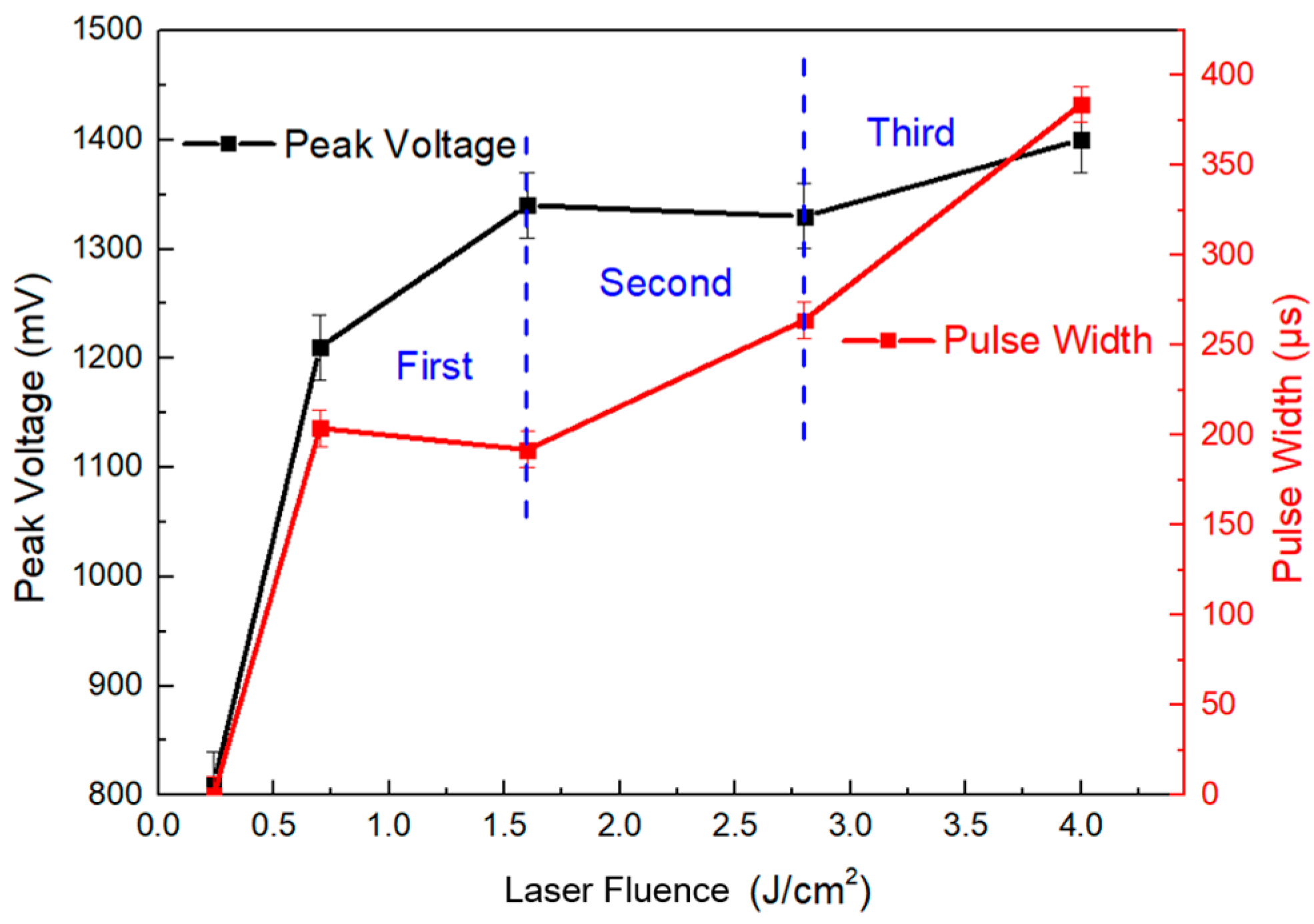
Figure 12.
Ablation morphology of laser-irradiated cells under different background light intensities.
Figure 12.
Ablation morphology of laser-irradiated cells under different background light intensities.

Figure 13.
Characteristics of Si cell’s electrical parameters under laser irradiation at different positions: (a) open-circuit voltage; (b) short-circuit current; (c) peak power.
Figure 13.
Characteristics of Si cell’s electrical parameters under laser irradiation at different positions: (a) open-circuit voltage; (b) short-circuit current; (c) peak power.

Figure 14.
The equivalent circuit of a solar cell.

Figure 15.
Parallel and series resistance of the Si cell under laser irradiation at different positions: (a) parallel resistance; (b) series resistance.
Figure 15.
Parallel and series resistance of the Si cell under laser irradiation at different positions: (a) parallel resistance; (b) series resistance.


Table 1.
Electrical performance parameters of the Si cell under laser irradiation.
| Laser Fluence (J·cm−2) | Output Voltage (mV) | Open-Circuit Voltage (V) | Short-Circuit Current (mA) | Peak Power (mW) |
|---|---|---|---|---|
| 0 | 820 | 1.24 | 200 | 174 |
| 0.24 | 820 | 1.24 | 204 | 176 |
| 0.76 | 820 | 1.24 | 207 | 175 |
| 1.6 | 780 | 1.22 | 203 | 153 (−12.1%) |
| 2.8 | 740 | 1.22 | 202 | 152 (−12.6%) |
| 4.0 | 720 | 1.18 | 205 | 137 (−21.3%) |
Table 2.
Electrical performance parameters of the Si cell under laser irradiation.
| Background Light Intensity (W/m2) | Open-Circuit Voltage (V) | Short-Circuit Current (mA) | Peak Power (mW) |
|---|---|---|---|
| 1100 (No laser) | 1.22 | 200 | 171 |
| 1100 | 1.14 | 200 | 145 (−15.2%) |
| 550 | 1.14 | 200 | 140 (−18.1%) |
| 0 | 1.12 | 202 | 129 (−24.6%) |
Disclaimer/Publisher’s Note: The statements, opinions and data contained in all publications are solely those of the individual author(s) and contributor(s) and not of MDPI and/or the editor(s). MDPI and/or the editor(s) disclaim responsibility for any injury to people or property resulting from any ideas, methods, instructions or products referred to in the content. |
© 2024 by the authors. Licensee MDPI, Basel, Switzerland. This article is an open access article distributed under the terms and conditions of the Creative Commons Attribution (CC BY) license (https://creativecommons.org/licenses/by/4.0/).
Share and Cite
MDPI and ACS Style
Li, S.; Huang, L.; Ye, J.; Hong, Y.; Wang, Y.; Gao, H.; Cui, Q. Study on Radiation Damage of Silicon Solar Cell Electrical Parameters by Nanosecond Pulse Laser. Electronics 2024, 13, 1795. https://doi.org/10.3390/electronics13091795
AMA Style
Li S, Huang L, Ye J, Hong Y, Wang Y, Gao H, Cui Q. Study on Radiation Damage of Silicon Solar Cell Electrical Parameters by Nanosecond Pulse Laser. Electronics. 2024; 13(9):1795. https://doi.org/10.3390/electronics13091795
Chicago/Turabian StyleLi, Sai, Longcheng Huang, Jifei Ye, Yanji Hong, Ying Wang, Heyan Gao, and Qianqian Cui. 2024. "Study on Radiation Damage of Silicon Solar Cell Electrical Parameters by Nanosecond Pulse Laser" Electronics 13, no. 9: 1795. https://doi.org/10.3390/electronics13091795
Note that from the first issue of 2016, this journal uses article numbers instead of page numbers. See further details here.