
Survey of Reliability Research on 3D Packaged Memory
by
 , ,
, ,
Shuai Zhou
1,2, 
Kaixue Ma
1,*,
Yugong Wu
1,
Peng Liu
2,*,
Xianghong Hu
2,
Guojian Nie
2,
Yan Ren
2,
Baojun Qiu
2,
Nian Cai
3,*,
Shaoqiu Xu
3 and
Han Wang
3 1
School of Microelectronics, Tianjin University, Tianjin 300072, China
2
China Electronic Product Reliability and Environmental Testing Research Institute, Guangzhou 510610, China
3
School of Information Engineering, Guangdong University of Technology, Guangzhou 510006, China
*
Authors to whom correspondence should be addressed.
Electronics 2023, 12(12), 2709; https://doi.org/10.3390/electronics12122709
Submission received: 12 May 2023
/
Revised: 10 June 2023
/
Accepted: 13 June 2023
/
Published: 17 June 2023
(This article belongs to the Topic Advances in Microelectronics and Semiconductor Engineering)
Abstract
:As the core carrier of information storage, a semiconductor memory device is a basic product with a large volume that is widespread in the integrated circuit industry. With the rapid development of semiconductor manufacturing processes and materials, the internal structure of memory has gradually shifted from a 2D planar packaging structure to a 3D packaging structure to meet industry demands for high-frequency, high-speed, and large-capacity devices with low power consumption. However, advanced 3D packaging technology can pose some reliability risks, making devices prone to failure, especially when used in harsh environmental conditions, including temperature changes, high temperature and humidity levels, and mechanical stress. In this paper, the authors introduce the typical structure characteristics of 3D packaged memory; analyze the reasons for device failure caused by stress; summarize current research methods that utilize temperature, mechanical and hygrothermal theories, and failure models; and present future challenges and directions regarding the reliability research of 3D packaged memory.
1. Introduction
A memory circuit, as an important component of an integrated circuit, is the most widely used, basic, general-purpose integrated circuit. It plays an extremely important role in the semiconductor industry. According to the principle of whether stored data are lost following power failure, memory can be divided into two categories: volatile memory and non-volatile memory. Volatile memory mainly includes DRAM and SRAM, and non-volatile memory includes EEPROM, EPROM, PROM, NOR FLASH, and NAND FLASH. With the rapid development of semiconductor manufacturing processes and materials, the internal structure of memory has gradually shifted from 2D planar packaging structures to 3D packaging structures. Well-known memory manufacturers, such as Samsung Electronics, Micron, and SK hynix, have further improved the performance of memory devices via the use of 3D packaging technologies, such as PoP (package on package) [1,2,3], CoC (Chip-on-Chip) [4,5,6], WLP (Wafer Level Package) [7,8,9], TSV (through-silicon via) [10,11,12], and Embedded Substrate [13,14,15], meeting the industry demands for high-frequency, high-speed, and large-capacity devices with low power consumption.
This review first introduces the structural characteristics of different 3D packaged memories. We then analyze the reasons for typical stresses that lead to failures in 3D packaged memory systems and the corresponding thermal, mechanical, and hygrothermal theories. Additionally, this review summarizes solder–joint fatigue life prediction models, focusing on their theoretical bases, applications, advantages, and disadvantages. Next, this review summarizes the research results of memory systems with CoC and PoP structures under mechanical stress, temperature stress, and hygrothermal stress loadings. Finally, we suggest future directions for researching the reliability of 3D packaged memories. This review suggests building a comprehensive research platform to facilitate software and hardware integration, establishing multi-dimensional simulation models, fully combining simulation results with experimental results to improve the accuracy of predictions, and conducting experimental research in high-stress environments to fully understand the applicability and limitations of memory devices.
2. 3D Packaging Structure of Memory
The feature size of the traditional Moore’s Law approaches the physical limits of what semiconductor technology is able to withstand, and simply reducing the feature size of 2D packaging is no longer a feasible way to meet market demands and develop new technologies. As products that adhere to Moore’s Law, three-dimensional packages have become a strong contender for the development of new technology. Three-dimensional packaging mainly comprises a vertical interconnection of multi-layer structures in the Z direction, stacking multiple chips or two-dimensional packages to achieve a higher assembly density, higher system performance, and a greater number of I/O pins [16,17]. There are two main ways to formulate a 3D packaging structure: 3D CoC (ChIP-on-Chip) and 3D PoP (package on package).
2.1. CoC (ChIP-on-Chip) Structure
The standard way to increase memory capacity is to stack the same type of memory chips in the same package and interconnect them using wire bonding (WB) and through-silicon via (TSV). Importantly, 3D NAND constitutes the most common 3D submarket in the industry and is most typically representative of CoC structures. Its layer-stacking technology can increase density by adding storage unit layers in a vertical direction [18,19]. The number of stacked layers is the most intuitive performance indicator in 3D NAND products. Thus, producing more than 200 layers of 3D NAND products has become a new goal for leading international memory manufacturers [20,21]. Compared to microprocessors, NAND production has improved processing limitations and led to the exploration of new ways of continuing to implement Moore’s Law. As early as 2014, Toshiba and SanDisk launched the first batch of NAND chips with 15 nm process technology [22,23], some of the smallest flash memory chips produced at that time, indicating that 2D NAND was approaching its processing limit. Since then, 3D NAND has become the preferred technology in the NAND industry due to its increased capacity and reduced costs, driven by manufacturers such as Samsung Electronics and Micron. Samsung Electronics, SK hynix, and Micron successively released 128-layer TLC 3D NAND devices in 2019 [24,25,26] and 176-layer TLC 3D NAND devices in 2020 [27,28]. In 2020, Kioxia released a 112-layer 3D NAND [29]. YANGTZE MEMORY in China has maintained a similar pace as international manufacturers, releasing a 64-layer 3D NAND in 2019 and bypassing a 96-layer [30] 3D NAND to launch a 128-layer 3D NAND in 2020 [31], which then became widely established in Xtacking architecture. Figure 1 shows a 3D NAND roadmap [32].
The internal structure of CoC packaging is mainly interconnected via two processes: WB (wire bonding) and TSV (through-silicon via), which are described below.
2.1.1. WB Interconnecting Structure
A 3D NAND device with a WB process can be approximately divided into the following five typical CoC structures [19]. (1) Spacer CoC structure: A passive silicon wafer is added between two chips with the same area as a spacer to form an overhang structure between the upper and lower layers of chips, leaving enough space for wire bonding to a solder pad (Figure 2a). However, using a spacer increases the height of the memory device, which affects its assembly density. (2) Double-sided spacer CoC structure: Chips and spacers are mounted on both sides of the PCB (Figure 2b) to reduce the negative impact of the spacer on the height of the device. However, this leads to more complex chip design, especially in the solder pad area. (3) Stair-shaped CoC structure: Chips with the same area are mounted without spacers and sequentially bonded with an insulating adhesive (Figure 3). This structure ensures the mechanical reliability of the chips, since their non-overlapping area is minimal compared to their length. Thus, the overall mechanical strength is not affected, and the top-layer chip will not exceed the overall center of mass. However, all solder pads must be located on the same side of the package, increasing the area on the opposite side of the solder pads. (4) Snake-shaped CoC structure: As another optimization solution for stair-shaped CoC structure, the overall size can be significantly reduced due to double-sided chip mounting (Figure 4). (5) Hybrid interconnecting process CoC structure: This CoC structure is similar to stair-shaped and snake-shaped structures but different in the interconnection direction of the upper and lower layers of the chips (front mounting and back mounting). The CoC structure is achieved by combining wire bonding and flip–chip interconnection or by using flip–chip interconnection alone (Figure 5).
Figure 6 is a cross section of Samsung’s 3D NAND device manufactured for the Apple iPhone, with a package thickness including a substrate of only 0.93 mm, a CoC height of 670 µm, and a chip thickness ranging from 55 to 70 µm, with the thickest chip located at the bottom [33]. Figure 7 shows Samsung’s solid-state drive (SSD), in which 16-layer and 48-layer V-NAND 3D flash memory chips are stacked using wiring bonding technology; each chip is only 40 µm thick and is stacked on an organic packaging substrate [33].
In the early days, the lead material in the WB process was mainly Au wire. However, due to the high cost of Au wire, and with the development of bonding technology for Cu and Al wire [34] (Figure 8), over 50% of the Au wire in the CoC interconnect structure has gradually changed to Cu, Al, and even Ag wire [35,36,37].
However, in traditional WB processes, it is necessary to maintain the ladder-like CoC structure of the memory chips and the bonding pad area on the packaging substrate after the 3D NAND memory chips are stacked into a ladder shape. Therefore, the number of stacked memory chips is limited, which indicates that storage capacity is restricted.
2.1.2. TSV Interconnection Structure
To further adhere to Moore’s Law, TSV technology has become a driving force for the development of 3D NAND products. The vertically stacked memory chips are electrically interconnected to each other via filling them with conductive materials, such as copper, tungsten, or polysilicon, or using metal–metal bonding to achieve silicon via holes. The bottom layer of the memory chip is connected to the packaging substrate via a metallized wiring layer and solder. Since there is no demand for interconnections with the bonding pad of the packaging substrate, the number of stacked memory chips can be increased. Compared with traditional WB, TSV technology has fewer restrictions, and it can further reduce signal delay and parasitic capacitance/inductance, achieve a low power consumption and high transmission rate, increase bandwidth, and realize product miniaturization. Although TSV technology has these advantages, it reduces the wafer area utilization and relative processing time of 3D NAND devices. Samsung Electronics used TSV and micro-bumps to release a 16 Gb memory (including eight pieces of 2 Gb memory chips) in 2006. The thickness of this stacked chip was 560 μm, smaller than the traditional 720 μm chip at that time. The stacked chips can either be NAND chips or DRAM chips [34], as shown in Figure 9.
In 2015, Toshiba released its first NAND product based on Bit Cost Scalable (BiCS) architecture, which was manufactured using a 48-layer stacked 3D NAND process combined with TSV technology. Although the number of stacked chips is maintained at 8 or 16 layers, the product was capable of providing a single capacity of 512 GB or 1 TB, indicating that the capacity of a single chip was 512 Gbit (64 GB) [19], as shown in Figure 10.
2.2. Package-Stacking Structure
Package stacking is an effective solution to the challenges involved with gradually reducing the size, cost, signal interference, and delays of chip devices. It also contributes to the low power consumption, high-speed information processing capacity, and large storage capacity of chips, which can improve interconnection efficiency and bandwidth. Package stacking can be divided into two main types: PiP (package-in-package) [38] and PoP (package-on-package) [39]. PoP is a 3D packaging technology that stacks two known good dies together. Since both the bottom logic device and the top memory device follow JEDEC’s electrical and mechanical standards, this standardized design enables different manufacturers to quickly design and produce products that are compatible with each other, achieving efficient package-stacking combinations. As a new packaging technology, PoP achieves a higher number of vertically stacked single (or various types of) devices on the basis of existing, compatible, standard surface mount technology, which can increase PCB assembly density and reduce production costs. Thus, it is rapidly becoming the preferred packaging method for many core components of smart portable electronic products, such as mobile phones, desktop computers, and smart watches. PoP technology was used in several Apple iPhones, from the iPhone 1 in 2007 to the iPhone 13 in 2021. In the Apple iPhone 12, the A14 processor made from a TSMC current sheet is stacked with Micron LPDDR4X SDRAM [40]. The widespread application of PoP technology has brought tremendous demand for PoP packaging devices. In 2021, global sales of high-end smartphones increased by 24% compared to those in the previous year, with a year-on-year increase of 7%. This strong market demand has further driven the continuous innovation and development of PoP technology.
2.2.1. PoP Structure
According to different interconnection modes inside the top and bottom stacked devices, PoP packaging can be divided into three typical structures: WB (wire bonding), flip–chip interconnection, and WB and flip–chip interconnection [41], as shown in Figure 11.
First-generation PoP technology typically integrates a baseband or application processor device and uses either a center gate mold or an exposed flip–chip die structure. A top single or combination memory package typically uses a peripheral two-row array of solder balls for stacking or the memory interface, using a ball diameter and pitch sufficient to provide a stacking clearance on the center mold or FC die [42], as shown in Figure 12.
Nokia and Amkor played key roles in the development of the first generation of PoP technology and reported early research on this technology at the 2003 ECTC conference [43]. ST Microelectronics was an early adopter of PoP for both memory systems and mobile processors. The background and history of the commercialization of first-generation PoP technology are summarized in a June 2007 article written by Smith and published in Semiconductor International [42].
Due to the vertical soldering interconnection between the two layers of PoP packaging, the Z direction is fully utilized to further reduce circuit PCB area to achieve a high packaging density. Moreover, a single packaging body can realize multiple functions. Figure 13 shows a typical application of a logic device and a memory device combination in a PoP package used in the Apple iPhone 5s [44]. The top package is a 1 GB LPDD3 RAM chip (11 mm × 7.8 mm) developed by Elpida (now Micron), which is internally interconnected using wire bonding via three rows of 456 solder balls in the FBGA (fine-pitch ball grid array) package substrate. The bottom package is a 64-bit A7 processor chip (10 mm × 10 mm), which is interconnected through 38 × 34 = 1292 solder ball bumps on the packaging substrate.
PoP packaging technology has been continuously developed and improved over the past decade in several different aspects. (1) Stricter control of warpage [45,46]: Due to the decreasing proportion of the packaging shell to the chip size (increasing in area) and the further improvement of system integration, warpage has become a more prominent issue and thus needs to be controlled. (2) More advanced interconnection methods: To reduce signal interference and transmission delay, traditional WB has gradually been replaced by flip–chip and copper pillar technologies. (3) Continuous reduction in structural size [47]: Firstly, the spacing between interconnections has been continuously reduced. Specifically, the spacing between the bottom packaging solder balls has been reduced to 0.5–0.2 mm, and the spacing between the top solder balls has gradually been reduced from 0.65 mm to 0.4 mm [48]. Secondly, the thickness of each layer of packaging material has been continuously reduced. The thicknesses of the substrate, EMC (epoxy molding compound), and the chip have been reduced from 0.3 mm to 0.13 mm, from 0.28 mm to 0.15 mm, and to below 0.1 mm, respectively.
Driven by the above trends, Amkor successively developed PSfcCSP (Package-Stackable Flip Chip Chip Scale Package) and TMV (Through-Mold-Via) technologies (as shown in Figure 14) [49] based on the traditional PSvfBGA (Package-Stackable Very Thin Fine Pitch BGA) technology [50].
TMV technology can penetrate molding compounds at the upper and lower interconnection welding points in a through-hole via, with the welding column vertically connected to the upper and lower packages for interconnection. The technology can not only reduce packaging warpage via plastic packaging materials but also further reduce the interconnection spacing between upper and lower solder balls by relying on the support and spacing of plastic packaging.
The development of advanced, next-generation FOWLP (Fan-Out Wafer-Level Package) technology [51] has fully addressed the shortcomings of the above technologies and been gradually applied in PoP packaging [44] (as shown in Figure 15). This technology often uses a rewiring layer on both sides of the package and a through-hole via to penetrate the plastic fan-out area at the package edge, reducing the package thickness to approximately 0.25 mm. Meanwhile, a high-density encapsulated interface technology with a pitch of less than 0.4 mm is applied to place multiple chips inside the package side by side, and to reduce the package spacing to about 0.15 mm. Ultra-thin PoP modules with a size of less than 12 × 12 mm and a height of less than 1.0 mm can be obtained using this technology.
2.2.2. PiP Structure
PiP (package in package) is a 3D packaging technology, also known as cube packaging technology, in which several known good devices are stacked in the same packaging cavity via a vertical welding interconnection. The manufacturer, 3D-Plus Ltd. (Versailles, France), has applied PiP technology to develop a radiation-resistant, large-capacity, and high-reliability 3D PiP memory for Galileo Program and other aerospace and aviation applications [52]. In 2001, it passed assessments by the ESA (European Space Agency), the CNES (Centre National d’Études Spatiales), NASA (National Aeronautics and Space Administration), and GSFC (Goddard Space Flight Center), with typical reliability test items shown in Table 1 and Table 2 [53].
The following technical process is shown in Figure 16. First, n-layer multi-device stacking and molding are carried out on two-dimensional packaging memory devices that have passed the test. Epoxy resin is then used for the casting mold, and the trim is cut off after the epoxy resin curing. After that, the packaging shell is sequentially electroplated, interconnected using laser grooves, surface coated, and pin molded. Finally, a large-capacity 3D PiP memory is formed [54,55]. The packaged 3D memory has a variety of packaging forms, such as SOP, QFP, and BGA (as shown in Figure 17 and Figure 18) [56,57]. This is mainly due to other types of internal encapsulated devices and the demand for different numbers of I/O devices.
This type of 3D PiP memory has strong anti-vibration and impact resistance, because the internal laminated units are fixed with epoxy resin. The surface of the packaging shell is plated with Ni/Au, with thicknesses of 1–2 μm for the gilded layer and 3–5 μm for the nickel plating layer. This metal plating can effectively reduce the invasion of water vapor or other harmful gases into the package. Moreover, the operating temperature range of this product can reach up to −55–125 °C, which is far larger than that of industrial/commercial 3D packaging memory products. In addition, its anti-radiation indicators, such as TID (total ionizing dose), SEL (Single-Event Latchup), and SEU (Single-Event Upset), also meet the requirements of relevant space missions, such as NASA’s Rover and China Aerospace Chang’e-5. Therefore, the 3D PiP memory developed by 3D-Plus Ltd. (Versailles, France) is widely used in various high-reliability fields.
In addition to 3D-Plus Ltd. (Versailles, France), O.C.E Technology Ltd. (Dublin, Ireland) and Orbita Aerospace Ltd. (Zhuhai, China) have also developed similar memory products for high-reliability applications. For example, Orbita Aerospace Ltd. (Zhuhai, China) developed a 128 K × 40 EEPROM (electrically erasable programmable read-only memory), which is composed of a lead frame layer and five chip layers. Specifically, external connection pins are arranged on the lead frame layer, and a memory device of the same type (128 M × 8 bit) is stacked on each chip layer. Five CSs (chip selects) of the internal device are simultaneously connected to an external pin of the chip, and other control and address signals are interconnected with each other and then to the external pin of the chip. Five sets of 8-bit data lines are led out independently. Finally, after the gilded connecting lines on the external surface are encapsulated and cut, the chip layer of the built-in device and the pin wiring of the lead frame layer are connected into a 3D-packaging 128 K × 40 bits SOP64-pin memory module. Its typical structural features are shown in Figure 19 and Figure 20.
For 3D memory modules encapsulated with epoxy resin, the NEO-stacking technology developed by Irvine Sensors Corporation can be used to stack chips of different sizes and types layer by layer [55] (as shown in Figure 21). The chip bumps (input/output ports) are rewired to both sides of the module through metallized film on known good devices. A passivation layer is deposited on the surface of the chips with polyimide, and then the chips are thinned and cut. After that, the multi-layer chips are stacked with adhesive and then pressed between the top and bottom ceramic substrates (aluminum oxide) [55], as shown in Figure 22. The rewired input/output ports are exposed on both sides of the lapping and polishing stack structure, and then the electroless plating process is used to form a coating (Cu/Ni/Au) on the stack structure. Finally, laser grooving is used to realize the electrical interconnection between the interior and the package or substrate [58].
3. Failure Reason Analysis of 3D Packaging Memory
During manufacturing and usage, 3D packaged memory modules are usually subjected to environmental stresses, such as thermal stress, mechanical stress, and hygrothermal stress. They are also exposed to cosmic radiation if used in space. According to the statistics from The Electronic Failure Analysis Handbook, 40% of the electronic component failures are caused by temperature changes, 27% by vibration, 19% by moisture, 6% by sand and dust, 4% by salt, 2% by shock, and 2% by altitude [59]. As shown in Figure 23, among the four factors affecting the reliability of electronic components, temperature, and vibration account for 69% of failures. The typical failure modes of electronic components under environmental stress are shown in Table 3.
3.1. The Influence of Thermal Stress on Reliability
Thermal stress usually refers to the change in thermal load caused by welding and ambient temperature. As most packaging materials are composed of multiple different materials, the differences in thermal expansion coefficients among the substrate, lead, chip, and epoxy resin of the device will cause thermal expansion and contraction, corresponding to the thermal expansion coefficient between different materials. However, due to the external packaging constraints or internal deformation coordination requirements, this cannot occur freely, and internal thermal strain produces delamination or cracks in the device [60,61]. In the interconnected structure of a 3D packaging memory device, in addition to the thermal expansion mismatch between adjacent materials, the internal stress and microstructure of the chip bump and solder joint are prone to changes under an environment of periodic alternating high–low-temperature or extreme-temperature gradients. This will lead to the accumulation of stress and strain inside the device, ultimately causing cracks or thermal fatigue failure in the solder joints [62,63].
3.2. The Influence of Mechanical Stress on Reliability
Mechanical stress usually refers to dynamic loads such as dropping, constant acceleration, vibration, and shock, which can lead to mechanical damage, such as the cracking and brittle fracture of products. Especially for electronic equipment components in aerospace fields such as space launch vehicles, missiles, and aircrafts, sine vibration during the launch process can reach up to 20 g [64]. Whether the structure and material strength of the device can withstand mechanical stress without damage and failure is a key factor affecting its reliability. Meanwhile, the 3D packaged memory mounted on the PCB or the substrate is subjected to vibration loads when vibration acts on the PCB, causing it to undergo a large bending dynamic deformation and exerting great mechanical cyclic stress on the interconnected solder joints. This mechanical stress will lead to mechanical damage and the fracture of the solder balls. For PoP memory, the vibration load acting on the PoP package can cause a large relative displacement between the upper and lower ends of the bottom solder ball, which makes the bottom solder ball bear the cyclic tensile stress of stretch–shrink mechanisms, similar to the spring oscillator. This tensile stress will lead to fatigue damage of the bottom solder ball [65]. It is noted that when the package is subjected to both dynamic and thermal loads, their interactions can accelerate crack propagation, greatly reducing the service life of the products.
3.3. The Influence of Hygrothermal Stress on Reliability
Industrial/commercial 3D packaging memory devices are mainly made from molding compounds, whereas aerospace or military 3D packaging memory devices are mainly made from metal or ceramic materials. Molding compounds are more hygroscopic than metal or ceramic materials; therefore, moisture has a greater impact on industrial/commercial 3D packaging memory devices and can change the distribution of thermal stress in these devices. Moreover, process-induced defects can make moisture more likely to enter the inside of the device via the small cracks forming along the device pins or the interface between the substrate and the plastic package. In particular, a high temperature will accelerate the penetration of moisture. Thus, moisture is one of the main reasons that plastic packaging devices were banned in early aerospace equipment. Generally, these devices are prone to galvanic cell corrosion and electromigration, which will potentially cause functional failures, such as short-circuit and open-circuit failures [66]. From a local perspective, moisture reduces the adhesive strength of various material interfaces, making interlayer delamination or cracking more likely to occur. Furthermore, the moisture inside the device can be converted into steam pressure during high-heat treatments (such as baking and reflow soldering), causing the generation of gas-induced cracks [67].
4. Reliability Theories for 3D Packaging Memory
A large number of studies address the reliability of 3D packaged memory devices based on the effects of thermal stress, hygrothermal stress, and mechanical stress.
4.1. Theories of Hygrothermal Stress on Reliability
Studies of hygrothermal stress mainly focus on moisture diffusion and wet stress distribution [68,69,70].
4.1.1. Moisture Diffusion
Moisture mainly enters the interior of the device package via a diffusion mechanism. Diffusion flux is defined as the material flow per unit of area passing vertically in a specific direction in unit time. Based on the relationship between diffusion flux and time, diffusion can be classified as steady state (unchanging with time) or unsteady state (changing with time). In 1855, A. Fick proposed Fick’s First Law, which states that the diffusion flux per unit area perpendicular to the diffusion direction is proportional to the concentration gradient at that point [71], formulated as follows:
where J, D, C, and x denote diffusion flux (kg/m2·s), diffusion coefficient (m2/s), concentration of the diffusate (kg/m), and diffusion distance, respectively. dC/dx is the concentration gradient of the diffusate. The negative sign indicates that the diffusion direction is opposite to the concentration gradient. In other words, diffusion occurs upon movement from a high-concentration area to a low-concentration area. The diffusion coefficient D is an important physical quantity that describes the diffusion rate and is equivalent to the diffusion flux when the concentration gradient is 1. The larger the value of D, the faster the diffusion.
However, Fick’s First Law is only applicable to steady-state diffusion situations where the diffusion flux does not change with time [71]. In fact, the diffusate concentration changes with time during the diffusion process, and most diffusion processes occur under unsteady conditions, where dC/dx ≠ 0. In order to study unsteady diffusion, Fick’s Second Law [71] was derived based on the theory of diffusion concentration equilibrium, formulated as follows:
where C is the diffusate concentration, which is also the distribution function of moisture concentration related to the spatial location (x, y, z) and time t, i.e., C = C (x, y, z, t). For three-dimensional diffusion problems, Fick’s Second Law is formulated as follows:
Since Dxx = Dyy = Dzz = D for the isotropic material, Equation (3) can be simplified as follows:
Due to various hygrometric coefficients of different materials, C at the junction of materials is discontinuous [72,73]. The concept of relative humidity W = C/Csat (Csat is saturated humidity) is commonly employed in research [74]; it is continuous at the junction of materials and follows Fick’s Second Law. Thus, Equation (4) is transformed as follows:
Since moisture diffusion and heat conduction share similar characteristics and follow the same mathematical control equations, temperature and thermal conductivity in the heat transfer equation correspond to moisture concentration and diffusion coefficients in moisture diffusion, respectively. Their analogous relationship [74] is shown in Table 4 [74]. Therefore, a thermal analysis module in finite element software can be used to analyze moisture diffusion, which can be used to calculate the moisture diffusion distribution of the device packaging model. This calculated moisture diffusion distribution can be applied as a moisture load to a packaging model to measure the distribution of moisture stress.
4.1.2. Moisture Stress Distribution
Generally, it is believed in the industry that water molecules absorbed by polymer materials exist in two forms [75]. One is in a free state, where free water molecules exist in the micropores of polymer materials. The other is the bound state, where hydrogen bonds are formed between the water molecular chain and polymer molecular chain in order to bind water molecules. Ardebili et al. identified two distinct modes of moisture absorbed in epoxy-like polymer materials using NMR spectroscopy [76]. Liu et al. confirmed hydrogen bonding between internal water molecules and epoxy resin by analyzing the infrared spectrum of epoxy resin in a high-temperature and high-humidity experiment [77]. Wong et al. analyzed the moisture expansion of polymer materials under the same test conditions for two identical products using a TMA (thermal mechanical analyzer) and TGA (thermal gravimetric analyzer). In order to measure the moisture absorption parameters of the fillers under a packaging molding compound together, two identical samples were pre-treated under the same humidity/temperature conditions in the experiment and then placed in a high-temperature furnace for high-temperature desorption. During the process, TGA was used to measure the loss of sample mass, whereas TMA was used to measure changes in sample geometry. Then, a relationship diagram was drawn between the strain and moisture concentration. The linear relationship between the two is known as the moisture expansion coefficient of materials [78]. In other words, the slope in Figure 24 refers to the moisture expansion coefficient β of polymer materials. The slope in Figure 24 represents the coefficient of moisture expansion (CME) of the polymer material, formulated as follows:
where C is the moisture concentration in the polymer material, and ε is the dependent variable of the sample. Wong et al. further verified Equation (6) according to experimental data and found that temperature T has no significant effect on the CME [79].
Therefore, after the moisture diffusion of a device is measured using finite element thermal analysis, the moisture stress distribution can be calculated via the CME and moisture diffusion coefficient D of the device material.
4.2. Theories of the Effect of Thermal Stress on Reliability
Studies on thermal stress mainly focus on the temperature field and thermal stress, whose goal is to calculate the temperature field and other thermal physical parameters of a system or component [80].
4.2.1. Temperature Field
The temperature field refers to the overall distribution of temperature at all points in a material system in space (or within an object), which is a quantity field expressed by the quantity function of spatial coordinates (x, y, z) and time t as follows [80]:
Equation (7) describes a three-dimensional non-steady-state (transient) temperature field, and thus three-dimensional non-steady-state (transient) heat conduction occurs in this temperature field. A steady-state temperature field is a temperature field that does not change with time, i.e., T = T(x, y, z), with three-dimensional steady-state heat conduction. For one- and two-dimensional temperature fields, a steady-state temperature field can be expressed as T = f(x) and T = f(x, y), respectively, and a non-steady-state temperature field can be expressed as T = f(x, t) and T = f(x, y, t), respectively.
In order to determine the temperature field within an object, a general equation for the temperature field, i.e., a differential equation of heat conduction, is required based on energy conservation, formulated as follows:
where p and c are the density (kg/m3) and specific heat capacity (J/kg⋅K), respectively. kx, ky, and kz are the thermal conductivities (W/m⋅K) in the x, y, and z directions, respectively. qv is the heating rate (W/s) of the internal heat source. If there is no internal heat source within the object, Equation (8) can be rewritten as follows:
Currently, the temperature field of a 3D packaging memory device can be formulated as a function achieved via finite element analysis, including the differential equation of heat conduction, boundary conditions, and initial conditions.
4.2.2. Thermal Stress
When the temperature of an object changes, thermal stress occurs due to the mutual constraints between the object and other objects that cannot freely expand or contract, or between different parts within the object. This is a type of stress caused by non-external forces, with temperature changes and constraints as its fundamental causes. The constraints can be classified into external deformation constraints, mutual deformation constraints, and internal deformation constraints. The internal structure of a 3D packaged memory is composed of chips, bonding wires, bumps, solder balls, substrates, and epoxy resin. Due to their different coefficients of thermal expansion, they are mutually constrained to each other as a whole device. When the device temperature changes, thermal stress will inevitably occur within the device. Stress is generated when thermal deformation cannot freely occur due to constraints or uneven temperature changes in various components of the device. Therefore, the device cannot completely expand and contract in a free manner, resulting in thermal stress due to the mismatch of thermal expansion coefficients of various materials, the uneven temperature transfer of the device, as well as its internal and external constraints. This linear strain can be regarded as the initial strain of the device. The equivalent nodal load (i.e., temperature load) can be calculated according to the initial strain. The nodal displacement induced by the thermal deformation can be obtained for thermal stress by solving the stress equation. Additionally, the comprehensive stress involving thermal stress can be achieved via a combination of the equivalent nodal load and other load terms. The thermal stress σ is described as follows [81]:
where D is the elastic matrix determined by the elastic constant of element material, ε0 is the current temperature strain, and ε0 is the initial temperature strain. For three-dimensional problems, ε0 is:
where α is the linear expansion coefficient of the material. Ø and Ø0 are the current/initial temperature fields of the structure, respectively. Thus, the principle of virtual displacement can be formulated as follows [80]:
The minimum potential energy for the thermal stress problem is formulated as follows [80]:
After the solution domain Ω is performed by finite element discretization, the finite element equation can be obtained from ∏p (u) = 0 as follows:
where K, a, and P are the element node force matrix, node displacement, and node temperature load, respectively. Thus, temperature load caused by temperature change is formulated as follows:
where Pf and PT are the load terms caused by volume load and surface load, respectively. Pε0 is the load term caused by temperature strain, formulated as follows:
4.3. Theories of Mechanical Stress on Reliability
The intrinsic characteristics (intrinsic frequency and vibration mode) of product structure are fundamental for dynamic research and analysis [82]. Mode analysis is carried out to obtain the intrinsic characteristics of product structure, such as intrinsic frequency and vibration mode, through which the relative changes in the positions of structural components under a vibration load can be calculated to determine the stress and response of the structure under a vibration load [82]. In practical engineering, mode analysis is commonly used for fixture analysis to avoid resonance. In research on mechanical stress, the known excitation force is applied to a product, which is the potential mechanical stress encountered in the operating environment and mainly entails random vibration, sinusoidal vibration, shock, and drop.
The response is measured to determine the dynamic characteristics of the product structure, such as the mode vector, damping, and frequency response. Compared with mode analysis, which focuses on the intrinsic characteristics of mechanical stress that are unaffected by external loads, the analysis of mechanical stress is closely related to external loads. A 3D PoP memory (PoP structure) device is a popular 3D packaged memory, which is commonly studied in the excitation modes of random vibration, sinusoidal vibration, and drop-induced shock.
4.3.1. Random Vibration
Random vibration refers to the motion in which the vibration rule can only be measured using probability and statistical methods instead of definite functions (sine and step) [83,84]. Due to the excitation load of random vibrations that cannot be expressed by a definite time function, the power spectral density function is often used to describe this excitation in engineering [85,86]. Random vibration analysis is employed to analyze the dynamic response of the structure under random vibration loads. The input for random vibration is the PSD (power spectral density) function, indicating the energy distribution of random vibration excitation loads at different frequencies. The corresponding output is the PSD response curve and the root mean square value of the response of a sampling point in the normal distribution interval and in each direction. In real applications, the vibration response characteristics of a product structure are generally evaluated via the comparison of root mean square values of input and output accelerations. The PSD function for random vibration is generally formulated as follows:
where f is the frequency, τ is the time difference between any two points during the process of random vibration, and R(τ) is the autocorrelation function of random vibration. Moreover, its PSD function and autocorrelation function can be used to form a pair of Fourier transform formulae as follows:
The autocorrelation function is used to describe the similarity degree of a random vibration process x(t) at different moments, formulated as follows:
The PSD function reflects the energy distribution of random vibrations in the frequency domain, involving unilateral and bilateral PSD functions. However, since negative frequencies do not exist in engineering, the bilateral PSD function has no intuitive physical significance at a negative frequency. Therefore, only a unilateral PSD function needs to be considered.
4.3.2. Sinusoidal Vibration
Sinusoidal vibration refers to a periodic reciprocating motion in which vibration parameters can be described using the sine function of the actual independent variables, also known as simple harmonic motion. Sinusoidal vibration analysis is used to analyze the dynamic response of harmonic loads to products. The input of sinusoidal vibration analysis is usually the acceleration amplitude of harmonic load in various frequency ranges, and the output is the corresponding acceleration–amplitude response curve. By comparing the acceleration–amplitude curves for the input and the output values, the response characteristics of the structure under sinusoidal vibration can be evaluated [87]. Since the sinusoidal vibration is a simple harmonic vibration, the instantaneous displacement signal of the particle from the equilibrium position can be described as a time-varying function when the particle vibrates in a sinusoidal manner along a straight line. Assuming that displacement (X) is a function of time t, the displacement amplitude of sinusoidal vibration can be formulated as follows:
where A, ω, and φ are the displacement amplitude, angular frequency, and initial phase. If the initial phase φ = 0, then:
After Equation (21) is differentiated, the corresponding velocity and acceleration can be obtained as follows:
As indicated in Equations (22) and (23), the velocity and acceleration signals for the vibrating particles are 90° and 180° ahead of the corresponding displacement signals, respectively. The velocity value is numerically proportional to the displacement, with the direction toward the displacement origin.
Assuming that the acceleration (g) is a function of time t, the acceleration of sinusoidal vibration can be formulated as follows:
where g0 is the peak acceleration. If φ = 0, then:
4.3.3. Drop-Induced Shock
When the product drops in free fall, its kinetic energy is mainly converted into thermal energy generated by friction, as well as the elastic and plastic strain energy of the product shell and internal components. Drop-induced shock analysis is mainly used to study the dynamic response and stress state of the product during the entire drop-induced shock analysis [88]. From the perspective of dynamics, the velocity before drop-induced shock depends on the drop height, formulated as follows:
where Vb, g, and h are the acceleration before drop-induced shock, gravitational acceleration, and drop height, respectively.
According to the momentum theorem, we can write the following:
where Va is the velocity after drop-induced shock, G(t) is the shock acceleration at time t, T is the shock duration, and m is the mass of the shock platform. Without other energy losses, Va is proportionate to the velocity Vb before rebound, formulated as follows:
where c is the resilience coefficient, whose value is between 0 and 1.
By substituting Equation (28) into Equation (27), we can write the following:
By substituting Equation (30) into Equation (26), the shock energy of the whole drop process can be obtained as follows:
5. Typical Models for Fatigue Life Prediction of Solder Joint
As a key part of various interconnected components of 3D packaged memory devices, a solder joint is used for electrical and mechanical connection, as well as a heat dissipation channel for the chip, whose reliability largely influences the quality of the product. When a solder joint is subjected to stresses, such as temperature cycle, vibration, and impact, strain accumulation can occur due to the mismatch of thermal expansion coefficients and different elastic moduli of various structural materials. This accumulated strain will result in the initial crack or new crack of the solder joint, causing it to continuously expand until fracture occurs, eventually leading to device failure [89]. Therefore, failure analysis and reliability research on solder joints is of great significance for 3D packaged memory devices. Nowadays, appropriate models for fatigue life prediction are widely studied after the stress–strain and energy density of solder joints of the device under environmental stresses are analyzed via finite element analysis [90,91]. In terms of various failure types of solder joints, fatigue life prediction models for solder joints are usually divided into four different categories based on plastic deformation, creep deformation, fracture mechanics, and energy. These models reflect the fatigue law of solder joints with different perspectives and accuracies and are for different applications that are suitable for fatigue life prediction under different stress conditions or failure types [92,93,94].
5.1. Fatigue Life Prediction Models of Solder Joints Based on Plastic Deformation
The representative life prediction models based on plastic deformation include the Coffin–Manson, Engelmaier, Soloman, and Norris–Landzberg models. These models are widely used to predict the low-cycle fatigue failure of solder joints due to cyclic plastic deformation, where stress–strain curves are generally plastic stress–strain curves. However, when these models are used for fatigue life prediction, they are easily affected by cycle frequency, the thermal expansion coefficient of chip packaging material, and stress type [95,96].
5.1.1. Coffin–Manson Model
The Coffin–Manson equation is the most commonly used life prediction model based on plastic deformation [97]. However, it ignores the effects of time and temperature on solder joint life. Based on the generalized fatigue damage law of metal materials [98], it is mainly applicable to low-cycle fatigue analysis caused by temperature loads [99] and is formulated as follows:
where , Δεp, c, and Nf are the fatigue toughness coefficients, plastic strain range, fatigue toughness index, and number of failure cycles, respectively.
5.1.2. Engelmaier Model
The Engelmaier model modifies the Coffin–Manson model to improve its effectiveness [100]. However, although it considers the influence of thermal cycle frequency and temperature on fatigue life, it does not consider the creep effect of solder joints [101,102]. Therefore, it is mainly applicable in situations where there are large differences between thermal expansion coefficients and the dominant shear stress–strain, formulated as follows:
where Δγ, f, and Tm are the range of shear strain, frequency of the thermal cycle, and average temperature of the thermal cycle, respectively.
The Engelmaier model can be widely used to predict the low-cycle fatigue failure of solder joints due to repeated plastic deformation. The involved stress–strain is mainly the plastic stress–strain. However, it is easily affected by cycle frequency, the thermal expansion coefficient of the chip packaging material, and stress type.
5.2. Fatigue Life Prediction Models of Solder Joints Based on Creep Deformation
Under high, low, or cyclic temperature conditions, creep effects related to loading time occur in solder joints. In microelectronic packages, for example, creep effects occur when the operating temperature of the solder joint exceeds half of the melting point of the SN-based lead-free solder. However, due to the complexity of the creep mechanism (creep, plastic, and elastic deformations overlap with each other in the creep process [103]), the model has limited accuracy in describing the creep process and ignores the influence of plastic strain [104].
5.2.1. Knecht–Fox Model
The Knecht–Fox model is a creep fatigue model based on the matrix dislocation theory [105], in which the solder microstructure is related to the creep shear strain range of the matrix. The model can be formulated as follows:
where Nf, C, and ∆γmc are the number of failure cycles, the material constant related to the microstructure of the solder, and the creep stress amplitude of the matrix, respectively.
5.2.2. Syed Model
The Syed model considers steady-state creep as the main cause of the thermal fatigue failure of solder joints, taking into account the cyclic creep fatigue life caused by varying and repeated stresses under a single creep mechanism [106,107]. The model can be formulated as follows:
where εacc and C′ are the creep strain accumulated in each cycle and constant reciprocal of creep ductility, respectively.
Equation (36) can be transformed into the energy density model as follows:
where wacc and W′ are the creep strain energy density accumulated in each cycle and the creep strain energy density at failure, respectively.
The Knecht–Fox model is a matrix creep model applicable to all packaging types, and the Syed model is a cumulative creep strain energy model mainly applicable to PBGA and SMD packaging. However, both models ignore the effect of plastic strain on solder joints during the temperature cycle, and plastic strain has a significant impact on the fatigue life of solder joints. This significantly limits the ability of the two models to predict the fatigue life of solder joints in electronic packaging.
5.3. Fatigue Life Prediction Models of Solder Joints Based on Fracture Mechanics
The Paris model and the J-integral model are representative fracture-mechanics-based models for the fatigue life prediction of solder joints [108]. Based on the fracture parameters, these models can predict fatigue life by calculating the damage caused by the accumulation and propagation of cracks. They consider the effects of strain energy dissipation and structural damage on fatigue life and establish a power relationship between the crack growth rate and the stress intensity factor. They are usually used under linear elastic fracture conditions and are only applicable to stable crack growth in fatigue tests.
5.3.1. Paris Model
The Paris model combines fatigue with fracture mechanics and uses stress intensity factors to describe the stress field strength at the crack tip, in which the stress intensity factor is considered the main cause of crack growth. The model can be formulated as follows:
where is the crack growth rate. N, a, and ∆k are the number of failure cycles, crack length, and amplitude of the stress intensity factor in each stress cycle, respectively. kmax and kmin are the maximal and minimal stress intensity factors in a load cycle, respectively. C″ and n′ are material constants, which are related to environmental factors, such as the temperature, humidity, medium, and loading frequency.
5.3.2. J-Integral Model
The J-integral model uses the J-integral as a mechanical control parameter. It mainly addresses cyclic plastic strain and is formulated as follows:
where c1 and m1 are material constants, and Sp is the area of the load–displacement curve in the case of a closed crack. B and W are the thickness and width of the sample, respectively. f(a, W) is a geometric function determined by a and W.
5.4. Fatigue Life Prediction Models of Solder Joints Based on Energy
The fatigue life prediction models based on energy mainly calculate the strain energy or strain energy density of each cycle according to the stress–strain hysteresis energy of solder joints in order to predict their fatigue life. There are two main methods to achieve this. One method is to directly predict fatigue life using empirical equations, such as those in the Akay model. The other method is to first predict the number of cycles when a solder joint initiates a crack and then calculate the crack growth rate according to fracture mechanics and the number of cycles when the crack growth causes the failure of the entire solder joint. Finally, these two values can be added together to obtain the fatigue life of a solder joint. The Darveaux model is representative of this second method.
5.4.1. Akay Model
The Akay model establishes the relationship between the average number of cycles in failure and the total strain energy, but it can only predict the cycle life at the time of solder joint crack initiation [109]. It is mostly used to predict the package in the form of a wired frame, which is formulated as follows:
where ΔWtotal is the total strain energy, and W0 and k are material constants.
5.4.2. Darveaux Model
Under the conditions of thermal stress or mechanical stress, the Darveaux model describes the relationship between the physical constants of solder joints and their actual life cycle based on the stress, strain, or energy between solder joints [110]. The fatigue process can be divided into two stages, namely, steady-state and nonlinear acceleration. In the steady-state stage, fatigue crack propagation occurs at a constant speed. In the nonlinear acceleration stage, the mechanical behavior of solder joints rapidly deteriorates. The Darveaux model is widely used for SnPb solder joint components and is suitable for the damage caused by crack initiation and propagation. However, there are many correlation coefficients in this model. Moreover, most solder joint failures occur only when the crack propagates to a certain extent, rather than when solder joints are completely broken [111]. These two factors limit the Darveaux model’s applications. The model can be formulated as follows:
where Ns, N0, ∆Wave, and a are the characteristic life cycles of interconnected solder joints, the number of crack initiation cycles, the average inelastic strain energy density accumulated in each cycle, and the characteristic fracture length, respectively. represents the crack growth rate. K1, K2, K3, and K4 are the coefficients obtained via the experiments and are related to crack propagation, finite element model structure, solder joint connections, and substrate material thickness, respectively.
6. Studies on the Reliability of 3D Packaged Memory
Packaging reliability is vitally important to ensure the normal operation of an entire electronic system. Studies on the reliability of 3D packaged memory devices are often carried out using a test analysis, finite element simulation analysis, or another comprehensive method. In the test analysis, device defects in reliability are simulated by environmental stress tests, and then the failure mode and mechanism for the device with defects are analyzed using various instruments and equipment. Common tests include mechanical tests (such as vibration, shock, and drop), thermal stress tests (such as temperature cycle and thermal shock), life tests (such as steady-state life and aging), hygrothermal stress tests (such as a steady-state hygrothermal test, highly accelerated steady-state hygrothermal test, and pressure cooker test), and space radiation resistance tests (such as dose rate reversal, dose rate induction locking, and electric dose). Relevant test standards and conditions can refer to several standards, including GJB548, GJB150, GB/T 2423, MIL-STD-202, MIL-STD-750, MIL-STD-883, JEDEC, and IPC. Typical reliability test items are shown in Table 5.
Finite element simulation analysis [112] is a method that uses computer-based finite element simulations to accurately identify defects in the devices and to optimize their designs. Meanwhile, it can also effectively simulate the stress distribution of the device in various environments, such as moisture distribution or thermal stress distribution. ABAQUS, ANSYS, and NASTRAN are commonly used finite element software programs in microelectronic packaging simulation analysis [113,114,115]. Finite element analysis fundamentally consists of preprocessing, simulation modeling, solving, and post-processing (Figure 25), in which material parameters and selected models are important for simulation accuracy.
The comprehensive method combines finite element analysis and test analysis, in which the former provides theoretical guidance for the test, which can then be used to verify and improve the simulated model. The analysis flow of the comprehensive method is shown in Figure 26.
6.1. The Reliability of PoP Memory under Thermal Stress
The thermal expansion coefficients of various materials in the package of PoP memory vary greatly, causing delamination or cracks to emerge inside the device due to the thermal strain induced by the change in thermal load. Especially under periodic high- and low-temperature alternation or extreme-temperature-gradient environments, the internal stress and microstructure of the chip solder joints inside the PoP memory are prone to change. With the passage of the time cycle, stress–strain accumulation will eventually lead to failures, such as solder joint cracks, package cracking, and delamination.
Zhang et al. [116] utilized temperature cycling loading (0–125 °C) and the Coffin–Manson model to analyze PoP packaging, indicating that the maximal accumulated inelastic hysteretic energy occurred in solder balls in the bottom FBGA (fine-pitch ball grid array) structure. In the FBGA structure, the thermal fatigue cracks originate from two symmetrical corners of the solder balls. The thermal fatigue damage in the outer array rapidly evolved into the inner array. By analyzing the failure data of solder balls, a thermal fatigue failure rule was defined, in which the critical failure probability was about 80%.
Wang Yang [117] carried out environment tests using off-line coupled temperature cycling and temperature shock on Amkor’s 14 mm × 14 mm and 15 mm × 15 mm PoP devices, obtaining strain values for the top chip and the bottom solder joints. Their results show a periodic variation in strain and stresses were mainly concentrated on the solder joints and chip. The maximal stress of the bottom chip was greater than that of the top chip. The stresses of the bottom solder joints were greater than those of the top solder joints on the whole, where the maximal value emerged in the corner of the outermost bottom solder joints.
Hongxia et al. [118] used Moiré interferometry to measure the thermal warping deformation of the BGA (ball grid array) in the upper and lower layers of the PoP devices during the reflux process. Then, they employed ATC tests and four-point bending cycle tests to analyze the reliabilities of PoP packages with different assembly processes under the same thermal warping deformation conditions. The results show that the top BGA has excellent reliability whether dipped in flux or solder paste, whereas the reliability of the bottom BGA dipped with solder paste is significantly lower than that of the printing process.
Tang Xiusheng [119] performed a simulation study on AmKor’s 14 mm × 14 mm PoP devices according to the load conditions of the temperature shock in the JEDEC standard. The results show that the stresses of the whole package under temperature shock were concentrated on the chip and solder balls, whose maximal value was found for the corner of the bottom solder ball. The stresses for the bottom solder balls gradually increased from the central solder ball to the marginal one, and the stresses for the top solder balls had no significant change trend. Finally, the Knecht–Fox model was used to predict the fatigue life of solder joints.
Chen et al. [120] used finite element simulation software to study the reliability of solder joints of eWLP PoP devices under −40–125 °C temperature cycle load conditions. The results show that the critical solder ball was located in the opposite corner of the bottom package, and the reliability of the solder joint could be improved by increasing the diameter of the solder ball and reducing the thickness of the bottom package.
From [116,117,118,119,120], it can be concluded that, in most research on the reliability of PoP packaging under thermal stress, a combination of finite element simulation, test verification, and solder joint fatigue life prediction formula was used to evaluate product reliability. Thermal stress loading is mainly based on thermal shock and temperature cycle test conditions, with the temperature loading condition of thermal shock in the range of −10–100 °C and the temperature loading conditions of the temperature cycle in the ranges of 0–125 °C, −10–100 °C, −55–125 °C, and −40–125 °C. The fatigue life of solder joints is greatly affected by different thermal stress loading conditions, such as temperature amplitude, residence time, and transition time. For example, [116,117,118,119,120] use a dual-layer PoP packaging device as the research object. According to the results of these studies, the weak-reliability areas of the product are mainly located in the bottom component and its outermost solder ball, which are also key areas of stress concentration. As shown in the research results of [116], the overall stress of the bottom solder joint is greater than that of the top solder joint, and the maximum stress of the bottom solder ball was found in the outermost corner solder ball of the fine-pitch ball grid array. Moreover, the results of the article [118] indicate that the stress of the entire package was concentrated on the internal chip and solder joints, with the maximum stress levels occurring at the corner solder joints of the fine-pitch ball grid array. In addition, the solder ball material, structural dimensions, stress distribution, and process of PoP packaging after assembly at the board level can also exert a certain impact on its reliability [118]. The common fatigue prediction models for solder joints include the Coffin–Manson and Knecht–Fox models. The main research results for PoP packaging under thermal stress are summarized in Table 6.
6.2. The Reliability of PoP Memory under Hygrothermal Stress
The packaging materials of the industrial/commercial PoP memory are molding compounds. Moisture levels can change the thermal stress distribution in a device, leading to galvanic cell corrosion, electromigration, and even functional performance failures in severe cases, such as short-circuit and open-circuit failures. Moisture can also reduce the bonding strength of each material interface, which turns into steam pressure in high-heat-treatment processes, resulting in the delamination between layers, which produces gas-induced cracks.
Hailong et al. [121] used a finite element simulation to study the influences of moisture stress introduced by hygroscopic expansion and thermal stress introduced during reflow on the reliability of PoP devices. The results show that the maximal hygrothermal–mechanical stress levels occurred in the corners of the marginal solder ball, and the hygrothermal–mechanical stress of the top package was larger than that of the bottom package.
Hailong et al. [122] utilized a comprehensive method to study the solder joint reliability of PoP devices, which combined finite element simulation with a high-temperature storage test and hygrothermal test. The results show that the hygrothermal test had no significant effect on the mechanical reliability of the components of the PoP device. However, under a high-temperature storage test, the components of the PoP device exhibited significant warpage, and the thickness of IMC became larger.
Guedon-Gracia et al. [123] proposed a comprehensive method combing numerical simulations and tests to predict the moisture induction effect in PoP devices and to analyze each component at the top and bottom of these devices. The results show that the overall moisture absorption of PoP devices was greater than that of the sum of two individual components. However, warpage deformation was less than either of the two individual components, resulting in many constraints inside the components.
Chen et al. [124] utilized a finite element simulation to study the reliability of PoP devices with an eWLP TMV structure under the conditions of 85 °C/85% RH, reflow soldering, and thermal cycling load. Additionally, they calculated the strain energy rate of delamination between copper and molding compound interfaces, comparing the performance and structural parameters of different materials. The results show that the critical position was located in the outer area of the solder pad under reflowing temperature and hygrothermal loads. The strain energy release rate of the delamination between copper and molding compound interfaces depends on the thermal expansion coefficients and elastic modulus of the molding compound. The strain energy release rate rapidly increased with the increase in CME. The strain energy release rate of the delamination at the outer layer of the copper pad sharply increased with the increase in the electrocoppering thickness. It also increased with the increase in electrocoppering pad length under a reflowing load. During the reflowing process, when the delamination length was less than 10 μm at 150 °C, it increased with the increase in the delamination length process and decreased with the increase in molding compound thickness.
To summarize [121,122,123,124], which researched the reliability of PoP packaging under hygrothermal stress, a combination of finite element simulation and test verification is mainly adopted to study the influences of hygrothermal stress introduced via hypersonic expansion, as well as thermal stress introduced during reflow welding processes, on the reliability of PoP packaging. The high-temperature and high-humidity loading conditions were 85 °C/85% RH and 168 h, and the loading condition of reflow welding was 260 °C. With the dual-layer PoP packaging device as the research object, as well as demonstrating the stress distribution of each component of PoP packaging, the results [121] indicate that hygrothermal stress is greater than thermal stress at the peak temperature of reflow welding, with a ratio of approximately 4:1. The results of [122] show that hygrothermal stress at 85 °C/85% RH has no significant effect on the warpage of PoP packaging. The results of [123] indicate that the overall moisture absorption of PoP packaging is greater than the sum of two individual components. The results of [124] indicate that hygrothermal stress increases with the increase in the length of the electrocoppering solder pad, and when the delamination length is less than 10 μm at 150 °C during the reflow load, it increases with the increase in delamination length and decreases with the increase in mold plastic thickness. The main results from the research on PoP packaging under hygrothermal stress are summarized in Table 7.
6.3. The Reliability of PoP Memory under Mechanical Stress
Microelectronic devices are often affected by external dynamic loads such as drop, vibration, and shock during usage and transportation, which can cause mechanical damage and destruction, such as cracking and brittle fractures. The reliability of electronic components in a device under vibration and shock loads is particularly critical for aerospace applications, such as airplanes, spacecraft, rockets, and missiles. Mechanical stress has little impact on the reliability of the 3D CoC structure NAND FLASH, since the packaging material is non-brittle, and the internal stacking units are fixed in epoxy resin without relative movable parts. Comparatively, it is sensitive to the reliability of the interconnected solder joints of the 3D PoP structure (DRAM at the top and CPU at the bottom), because the interconnected solder joints provide mechanical support and electrical interconnections in the PoP package. Under stress loads such as vibration, shock, and drop, cracks easily emerge in the stress concentrations inside the solder joint, which eventually cause the failure of solder joints. Therefore, many reliability studies on PoP structures focus on interconnected solder joints.
Jiang et al. [125] combined a vibration test and finite element analysis, which could characterize the fatigue characteristics of a PoP package under the vibration load, to obtain the stress–life (S–N) curve of PoP-packaged solder joints in Amkor’s double-layer PoP devices. They confirmed that the reliability of the bottom PoP package was significantly weaker than that of the top package, and thus the bottom solder ball was easily damaged under vibration loads. A random vibration fatigue life prediction model was also established for PoP-packaged solder joints and evaluated based on random vibration fatigue tests.
Yang et al. [126] employed sine vibration excitation to study the fatigue characteristics and reliability of PoP packages under vibration loads. Based on fatigue load spectrums under different excitation conditions, the strain amplitude and duration were calculated using the rain-flow counting method. Additionally, the strain–life (S–N) curves of a PoP package under different loads were predicted using a vibration fatigue life prediction model, providing an alternative to the optimal PoP design.
Haili et al. [127] used ANSYS modeling for the stress–strain analysis of random vibration stress on solder joints in PoP devices. The influences of some packaging parameters on the interconnection reliability were analyzed, involving the diameter, height, and PCB thickness of solder balls at the bottom of the PoP package. The results show that the maximal stresses of the bottom/top packages occurred at the corners of the marginal outer solder balls and at the corners of the innermost solder joints, respectively. They also pointed out that the maximal stress of the top package was the maximal stress of the entire package.
Zhaoyun et al. [128] employed a thermostatic compression test to determine the Anand visco-plastic constitutive model parameters for Sn-3.0Ag-0.5Cu solder. Then, these parameters were utilized to establish a finite element model of the PoP package for a reliability study on PoP-stacked packaging under different loads via direct coupling of thermal cycling and random vibration. The results show that, under random vibration, the maximal stress of solder joints increased with the increase in temperature and decreased with the increase in holding time. Additionally, the stress distribution of solder joints at high temperatures was affected by thermal stress and deformation during the thermal cycle, and the overall stress moved from the middle parts of the inner solder joints to the outer parts.
Based on the JEDEC standard, Fan Zerui [129] used ABAQUS software to construct five finite element models for PoP package components, which could analyze the influences of PCB damper, as well as the shapes, materials, and diameters of solder joints on the dynamic responses of package components during drop-induced shock. The results show that the maximal normal tensile stress of solder joints decreased with the increase in PCB damper and solder joint diameter. The maximal normal tensile stress of truncated, spherical solder joints was larger than that of cylindrical solder joints. The maximal tensile stress of lead-free solder joints was larger than that of SnPb solder joints. For lead-free solders, the maximal tensile stress of corner solder joints decreased with the increase in tin content.
Xiaohu et al. [130] simulated the dynamic response of PoP package components under drop-induced shock using the finite element method and analyzed the failure mechanism of solder joints. The results show that the repeated bending deformation of PCB was the fundamental reason for solder interconnection failure. The maximal tensile stress of lead-free solder was larger than that of lead solder. Additionally, the tensile stress at the lead-free corner solder joint decreased with the increase in tin content.
To summarize [125,126,127,128,129,130], which researched the reliability of PoP packaging under mechanical stress, a combination of finite element simulation, test verification, and solder joint fatigue life prediction formula was adopted to evaluate the reliability of PoP packaging under mechanical stress. Mechanical stress loading is measured under various experimental conditions, such as random vibration, sinusoidal vibration, drop, and thermal–vibration coupling. Different stress loads are selected according to different application scenarios. The random vibration mainly simulates environmental adaptability under the environmental conditions of highway transportation. The test conditions (severity) are jointly determined by parameters including frequency range, power spectral density, total root mean square acceleration, and test duration. For example, the test conditions of [125,127] are frequency ranges of 20–2000 Hz and 15–2000 Hz, power spectral density values of 0.08 g2/Hz and 0.04–0.05 g2/Hz, and a root mean square acceleration of 10 grms and 9.81 grms. The research results are essentially consistent: the maximum stress of the bottom component occurs on the outer solder ball, which is a weak area of reliability. Sinusoidal vibration mainly simulates the vibration capacity sustained in the process of launching, installation, and use. The test conditions (severity) are jointly determined using a vibration frequency range, vibration quantity, and test duration (times). For example, the test conditions of [126] include a frequency range of 100–2000 Hz, amplitude of 1 G, and a one-time duration of 20 min in order to analyze the dynamic response characteristics and stress distribution in PoP packaging components under a sinusoidal vibration load. The results indicate that transmissibility will decrease with the increase in natural frequency. Under the same cycle times, the higher the order of magnitude of input, the lower the reliability. The drop mainly simulates environmental adaptability under the condition of free fall from a certain height. For example, in order to analyze the dynamic response characteristics and stress distribution of PoP packaging components during the entire impact process, the test conditions of [129,130] are 1500 G and a half sine pulse duration of 0.5 ms. The research results are essentially consistent: the maximum normal tensile stress of solder joints decreases with the increase in PCB damping and solder joint diameter. The maximum normal tensile stress of truncated spherical solder joints is greater than that of cylindrical solder joints. Moreover, the maximum tensile stress of lead-free solder joints decreases with the increase in tin content, and the maximum tensile stress is greater than that of tin–lead solder joint. The main research results for PoP packaging under mechanical stress are summarized in Table 8.
6.4. The Reliability of CoC Package Memory under Thermal Stress
Similar to the PoP package, the thermal expansion coefficients of various materials vary greatly in the CoC package memory, which results in thermal strain due to thermal load. This thermal strain eventually results in delamination or cracks inside the devices. In the cases of periodic high–low temperature alternation and extreme temperature gradients, the internal stress and microstructure of chip solder joints in the CoC package are volatile to changes. With the passage of the time cycle, stress–strain accumulation will eventually lead to failures, such as solder joint cracks, package cracking, and delamination.
Zhang et al. [131] calculated the influences of different factors on the stress–strain response and fatigue life of 3D CoC package structure solder joints and Sn-3.9Ag-0.6Cu solder joints, which involved high temperatures, low temperatures, residence time of the thermal cycling load, and different IMCs. The results show that the maximal stress–strain occurred at the second solder joint on the diagonal of the IMC solder joint array. For a Sn-3.9Ag-0.6Cu solder joint array, the corner solder joints experienced maximal stress–strain at the locations of crack growth. The stress–strain and fatigue life of solder joints are more sensitive to residence temperature, especially in high-temperature environments. Increasing high-temperature strain and residence time or decreasing low-temperature strain could reduce stress–strain levels and prolong the fatigue life of solder joints.
Jiang et al. [132] employed X-ray diffraction (XRD) analysis to study the influence of high-temperature storage on the internal and peripheral stress of TSV in 3D CoC packaging. The results show that, in the stress distribution of copper-through holes and surrounding silicon before and after high-temperature storage, the binding forces of both copper and silicon were reduced, and high-temperature storage could accelerate the aging of copper and silicon for their long-term reliability.
Based on the TSV structure in the 3D CoC package, Tsai et al. [133] employed a finite element simulation to study the TSV thermo-mechanical stress distribution under temperature cycling load. The results indicate that the maximal thermal stress occurred in the external region of the TSV interface and the annular region of the TSV. Additionally, they obtained the thermal stress distribution of the TSV, which is beneficial for determining the possible failure regions of the device.
Yuwen et al. [134] established a seven-layer 3D memory CoC model and used the finite element method to simulate and evaluate the influence of thermo-mechanical stress on the internal TSV structure and interface reliability. The results indicate that stress was mainly concentrated at the chip and PCB interface on the copper side due to the larger thermal expansion coefficient and lower yield strength of copper compared to silicon. The structural parameters of TSV had a certain influence on interfacial stress. When the diameter ratio of TSV to copper nail remained unchanged, the maximal interfacial stress increased with the decrease in TSV diameter.
Zhang et al. [135] employed ANSYS software to analyze metal bumps in a 3D CoC package (CPU + RAM) and evaluate the reliability of the product in the temperature cycle. The results show that the plastic strain of Von Mises stress increased with the increase in the number of stacked chips. The metal bumps in the bottom layer had larger plastic strain levels than those in the top layer, and the outer metal bumps had larger plastic strain levels than the internal metal bumps.
To summarize [131,132,133,134,135], which researched the reliability of CoC packaging under thermal stress, a combination of finite element simulation, test verification, and accelerated life prediction formula was adopted to analyze the product reliability. Thermal stress loading is usually carried out under two test conditions: high-temperature storage and temperature cycling. The temperature loading condition of high-temperature storage is 150 °C, and the temperature loading conditions of temperature cycling are usually −55–125 °C and −40–125 °C. Under different conditions, such as temperature amplitude, residence time, and conversion time, different failure mechanisms will be generated for products. As shown in the research results of [132], a high temperature of 150 °C and time of 450 h can reduce the binding force of copper and silicon in TSV and thus accelerate aging. The research results [131,133] are essentially consistent: the maximum thermal stress is at the corner of the solder ball array. The results of [134] indicate that the residual thermal stress is mainly located at the interface between the TSV chip and PCB at the bottom, and the stress at the outer corner of the TSV array is significantly higher than that at the central position. The results of [135] indicate that the Von Mises plastic strain increases with the increasing CoC number, and the Von Mises plastic strain at the external metal bumps is greater than that at the internal metal bumps. Generally, for CoC packaging with the same structure, it is necessary to pay attention to the CoC number, TSV structure size, and stress distribution of solder joint arrays in a thermal stress environment. The main research results of CoC packaging under thermal stress are summarized in Table 9.
6.5. The Reliability of CoC Package Memory under Hygrothermal Stress
The packaging material of a CoC package memory is usually a molding compound. Moisture entering into the package will reduce the bonding strength of each material interface, especially during reflow soldering, which results in delamination between layers and gas-induced cracks. In addition, moisture also changes the thermal stress distribution of the device, leading to galvanic cell corrosion and electromigration and even functional performance failures, such as short-circuit and open-circuit failures.
Yu et al. [136] used Abaqus software to simulate the relative moisture diffusion distribution of a double-layer CoC packaged device (CPU + DDR) under 85 °C/RH 85% hygrothermal circumstance, as well as the distributions of moisture stress, thermal stress, and hygrothermal stress during reflow soldering after 168 h of moisture absorption. The failure mechanism of the device under hygrothermal circumstances was analyzed via absorption and reflow soldering tests. The results show that the bonding layers between the substrate and the components of CPU, CPU, and DDR cannot easily absorb moisture under hygrothermal circumstances. The moisture absorption of the bottom bonding layer was higher than that of the top bonding layer. After 168 h of moisture absorption, moisture stress was mainly concentrated on the long side of the DDR chip far from the center under a reflowing load. The maximal hygrothermal stress, as well as the thermal stress, were located at the corner of the bottom CPU chip: approximately 1.3 times the value of the pure thermal stress.
Zhu et al. [137] used a finite element simulation to establish a model involving moisture diffusion and hygrothermal–mechanical stress for double-layer CoC packages, which was utilized to analyze the characteristics of moisture diffusion. They combined the model with reflow soldering tests to study the effect of hygrothermal stress on the interlayer delamination of double-layer, chip-stacked packaging. The results show that the maximal stress occurred at the corners of the bottom chip.
Hua et al. [138] used a finite element simulation to analyze the water vapor diffusion characteristics of four-layer CoC devices under different test conditions in the JEDEC standard, as well as thermal stress during reflow soldering. The results show that the substrate and the bottom adhesive were subjected to high thermal stress and strain, together with high water vapor diffusion.
Anlin et al. [139] combined a finite element simulation and test analysis to analyze the influences of moisture diffusion and hygrothermal stress on the reliability of CoC devices. A finite element simulation of moisture absorption and soldering desorption processes was conducted under two sets of conditions: 192 h of moisture absorption at 30 °C/RH 60% and 168 h of moisture absorption at 85 °C/RH 85%. The moisture diffusions at different interfaces were analyzed to yield the influence rule. The combined hygrothermal stress was calculated using a hygrothermal coupling method and compared with the simple thermal stress. The results show that, similar to thermal stress, the maximal hygrothermal stress always occurred in the intersected regions between the top chip and spacer, with 1.3–1.5 times the value of pure thermal stress.
Wang et al. [140] conducted a finite element analysis to study the comprehensive influences of vapor pressure, moisture absorption swelling, and thermal expansion on the reliability of a two-layer CoC package during reflow soldering. The results show that after 168 h of moisture absorption at 30 °C/RH 60%, the CoC package essentially became saturated. The moisture desorption during reflow soldering was faster than pre-treatment moisture absorption. The maximal stress occurred between the bottom chip and the chip interconnection. Hygroscopic expansion and internal vapor pressure had significant effects on stress. The effects of comprehensive stress and warpage were much larger than those observed for a single stress.
To summarize [136,137,138,139,140], which researched the reliability of CoC packaging under hygrothermal stress, a combination of finite element simulation and test verification is mainly adopted to study the influence of wet stress introduced by moisture absorption expansion and thermal stress introduced during the reflow welding process on the reliability of CoC packaging. The high-temperature and -humidity loading conditions are 85 °C/85% RH, 168 h, 30 °C/60% RH, and 96 h. Moreover, the loading condition of reflow welding is 260 °C. The research results of [136,139] are essentially consistent: the hydrothermal stress is on average about 1.3 times higher than thermal stress [138]. In the CoC packaging with spacers, the suspension area between the top chip and the spacer was susceptible to high stress concentrations, which is a unique phenomenon of CoC packaging. The results of [136,137] indicate that the reliability of the bottom layer is lower than that of the top layer in a hygrothermal environment. As for moisture absorption, the results of [136] indicate that moisture absorption between the substrate and bonding layers of each chip is much lower than that of the plastic packaging material, and the moisture absorption of the bottom bonding layer is higher than that of the top bonding layer in a hygrothermal environment. The results of [136] show that the substrate and bottom adhesives are rapidly absorbed during a moisture diffusion simulation. The main research results of CoC packaging under hygrothermal stress are summarized in Table 10.
6.6. The Reliability of PiP Memory
Research on the reliability of 3D PiP memory, with radiation resistance, a large capacity, and high reliability manufactured by 3D-Plus (Versailles, France), O.C.E Technology Ltd. (Dublin, Ireland), and Orbita Aerospace Ltd. (Zhuhai, China), focuses on PCB-level assembly in the industry. Comparatively, only a few studies focus on comprehensive reliability by combining simulations with tests under the conditions of mechanical, thermal, and hygrothermal stress.
Qiang [141] used a finite element simulation to analyze the equivalent stress and equivalent plastic strain of 3D-Plus memory PCB components under random vibrations and temperature cycling. The results show that the design of the PCB screw fixation points was vital to the reliability of 3D-Plus memory PCB-level assembly. Reinforcing with epoxy adhesive could further improve the reliability of device assembly. The 3M-2166Gray epoxy adhesive with a high expansion coefficient can adversely affect the thermal fatigue life of solder joints. However, as long as the gap between the device pin and the PCB was controlled within 0.1–0.2 mm, with the solder at the root of the pin fully climbing during the welding process, a highly reliable solder joint could be obtained.
Bao et al. [142] used a nonlinear finite element analysis and plastic-ANAND model to evaluate the influences of Sn63pb37 tin–lead solder and Sn95.5Ag3.8Cu0.7 lead-free solder on the reliability of 3D-Plus memory solder joints. They calculated the stress–strain distribution and the potential failure locations of solder joints using a temperature cycling test. The results show that the stress and plastic strain of solder joints exhibited significantly frequent trends. The stress–strain curves tended to increase over time and eventually stabilized. When comparing the two equivalent stress and plastic strain curves of lead-free solder and tin–lead solder, it was found that the reliability of Sn95.5Ag3.8Cu0.7 solder was better than that of Sn63Pb37 solder.
Shuai et al. [143] employed a finite element simulation and thermal shock test to evaluate the reliability of solder joints of 3D PiP memory. The results show that the main failure mechanism of solder joints was thermal fatigue failure, and cracks were caused by the accumulation of plastic and creep strain. The initiation and propagation of cracks were mainly affected by the accumulation of inelastic strain, and the change trend was affected by the differences in thermal expansion coefficients between the epoxy resin and the chip.
Plante et al. [144] conducted tests of temperature, humidity, electrical stress, vibration, and shock to further stimulate the reliability defects of 3D-Plus memory. All the tests were implemented based on studies by the ESA (European Space Agency) and the CNES (Centre National d’Études Spatiales). The results show that such memory devices can operate normally in the temperature range of −55–125 °C, and they can withstand high-order mechanical stress and humidity, which far exceeds the resistance of industrial/commercial 3D packaging memory products. Dargines et al. [145] conducted anti-radiation tests, such as TID (total ionization dose) and SEE (single-event effects), on 3D-Plus memory to evaluate the reliability of the device in space applications. The results show that the device could withstand a TID of 100 Krad (Si) and a SEE of 60 MeV/mg·cm2, meeting the requirements of relevant space applications.
In [53,141,142,143,144], the reliability research of PiP packaging is mainly carried out via a combination of finite element simulation and test verification, but the number of research topics classified as thermal stress and hygrothermal stress is relatively lower than those classified as PoP and CoC packaging. In addition, due to the internal encapsulation structure of PiP packaging devices and the absence of movable components, reliability research on mechanical stress is only carried out after assembly at board level. Such studies include analyzing the equivalent stress and plastic strain of printed board components of 3D-Plus memory under random vibrations and temperature cycling [141]. In terms of the reliability of solder joints subjected to thermal stress loads, the results of [142] show that there is a significant periodic change in the stress and plastic strain of solder joints, and the reliability of lead-free solder is greater than that of lead-based solder. The results of [143] show that thermal fatigue is the main cause of solder joint failure, and cracks are caused by the accumulation of plastic strain and creep strain. The results of [53,144] indicate that the product can withstand high-order tests of mechanical stress and thermal as well as anti-radiation tests, including the total ionization dose (TID) and single-event effects (SEE), and thus it is suitable for high-reliability applications. The main studies on the reliability of PiP packaging are summarized in Table 11.
6.7. Discussion of Typical Formulae for Predicting the Fatigue Life of Solder Joints
From Table 6, Table 7, Table 8, Table 9, Table 10 and Table 11, it can be seen that the research achievements of the above scholars can improve the manufacturing technology of solder joints and play an important role in extending the fatigue life of solder joints. The overall situation is analyzed as follows. Application scenarios are mainly applied in thermal (thermal shock, temperature cycle) and mechanical stress environments (sinusoidal vibration, random vibration). There are two main types of fatigue life prediction models for solder joints: the plastic deformation fatigue prediction model and the creep deformation fatigue prediction model. However, there are few fracture parameter fatigue prediction models and energy fatigue prediction models. The Coffin–Manson model is the most common plastic deformation fatigue prediction model (e.g., [116]), and there are other less common models, such as the Ostergren, Miller, and Engelmaier models. The Knecht–Fox model is the most common creep deformation fatigue prediction model, as shown in the [117,119,126], whereas the Syed model is less common. The plastic deformation fatigue prediction model focuses on the mechanical parameters of the plastic deformation of solder joints, and this deformation has no positive correlation with time. The shear variable and correlation coefficient are substituted into the corresponding formula to obtain the number of cycles experienced during the final failure of components. Creep occurs when electronic components and solder joints undergo alternating low cycles and high temperatures. The creep deformation fatigue prediction model only considers the influence of creep on the reliability of solder joints, but it ignores the influence of other factors on the fatigue life of solder joints. Therefore, the prediction of the life cycles of solder joints is only suitable for some cases where creep deformation is the main cause of failure. The generation and accumulation of creep is very complicated. In addition, this type of model cannot fully express the whole creep process without considering plastic deformation, and thus it has certain limitations.
6.8. Current Reliability Research on 3D Packaging Memory under Multi-Stress Coupling
As mentioned above, domestic and foreign scholars have conducted in-depth research on the influence of a single loads on 3D packaging devices. Moreover, they have made great progress in formula model selection, experimental design, and subsequent verification. However, it is impossible for electronic products to be used under a single load. In order to accurately analyze their reliability, it is necessary to simulate and design a working environment that is compatible with their actual service. Therefore, it is very essential to study the influence of two or more coupling loads on the reliability of 3D packaging devices. Based on the theory of elastic–plastic fracture mechanics, Fan et al. [145] used a finite element simulation and numerical analysis to evaluate the influence of multiple cracks and thermal–mechanical coupling loads on the reliability of a TSV microstructure and studied the influence of crack number, crack location, crack length, crack direction, and thermal stress on crack growth. Han et al. [146] used a finite element simulation to study the stress–strain distribution of 3D-packaging CSP solder joints under temperature–vibration coupling loads. Meanwhile, they also carried out a sensitivity analysis on the influence of solder joint shape parameters on the maximum equivalent stress. Sijia et al. [147] used a finite element simulation to conduct electric–thermal coupling analysis of 3D CoC TSV structure and further studied the effects of different through-hole diameters and through-hole heights, as well as the effects of dielectric-isolation-layer SiO2 thickness on the current density, temperature field, and thermal stress distribution of the through-hole of TSV. Zhao et al. [148] used a finite element simulation to analyze the influence of wet–thermal coupling loads on the reliability of 3D CoC packaging and analyzed the influence of welding balls of different structural sizes on the reliability of packaging.
In Table 12, the most important research results on the reliability of 3D packaging memory under multi-stress coupling are summarized. Since thermal stress and mechanical stress are the two most important factors for the reliability of electronic components, [145,146,147,148] show that the reliability of 3D packaging memory under thermal–vibration coupling loads is a popular research topic. However, the fatigue life of solder joints under thermal stress and mechanical loading, for example, is not accurate according to the damage stacking method. This is because when multiple stress conditions exist at the same time, failure mechanisms are relatively complex, together with no accurate failure model. Therefore, the calculation methods of loading sequence and fatigue life require further study.
7. Discussion
Many factors affect the reliability of 3D packaged memory, involving the inherent characteristics of memory devices, such as packaging and injection materials, wire-bonding materials, structural sizes of chips and bumps, the array structures of solder joints, and the conditions of the working environment, such as temperature, vibration, and other stresses. At present, comprehensive methods combining finite element simulations and tests are dominant methods for studying the reliability of 3D packaged memory. Appropriate life prediction models for solder joints and failure analysis methods are used to predict the life of 3D packaged memory and to analyze its stress distribution, possible failure regions, and failure mechanisms. To some extent, these models can provide theoretical bases for structural designs and reliability applications. Although a large number of studies have focused on the reliability of 3D packaged memory, some issues have received little attention from researchers, as summarized below.
There is a lack of diversity regarding research objects. The research on 3D packaged memory mainly focuses on PoP and CoC structures. For PoP structures, most studies employ double-layer PoP products manufactured by Amkor Technology in reliability research, whereas only a few studies focus on the PoP memory devices manufactured by other companies and multi-layer PoP structures. Few institutions and researchers have studied the reliability of cube-packaging memory devices, except for NASA and ESA at an early stage. This lack of diversity is potentially due to the characteristics of 3D packaged memory devices, such as a long-term manufacturing cycle and limited access, since they are commonly used in high-reliability fields. There are also few testing methods for functional performance. Most researchers use daisy-chain circuits and resistance strain gauges to monitor the electrical properties of 3D packaged memories under stress loads for failure tests, which results in a low accuracy and repeatability of tests. In order to perform electrical parameter tests for 3D packaged memory devices, the researcher should be familiar with the structural characteristics of the product and have the ability to develop test procedures and to design test boards. Additionally, high-end testing equipment, such as ATE, is preferred for tests. However, many universities and non-device-manufacturing enterprises are not equipped with sufficient hardware and experienced researchers. Furthermore, test conditions are closely related to the failure mechanisms of a device, which involve temperature range, switching time, residence time, and moisture strength. Due to the fact that most 3D packaged memories are currently used in civil fields, such as mobile phones, smart watches, and mobile hard disks, most researchers choose test conditions based on the industry or civilian standards, such as JEDEC and IEC, rather than severe military standards, such as MIL and GJB.
There are various reliability concerns regarding devices with different 3D packaging structures. For PoP packaging of the same structures, it is necessary to pay special attention to the stress distribution of the bottom component and the outermost solder ball of the bottom component under thermal stress and mechanical stress. Moreover, the material and structural size of a welding ball and the stress distribution of the product after mounting the coupling plate also require future study. In a hot and humid environment, it is also necessary to pay attention to the moisture absorption of each component. For CoC packaging of the same structure, in a thermal stress environment, it is necessary to focus on the number of stacked chips, TSV structure size, and stress distribution of solder joint arrays. Meanwhile, the differences in temperature amplitude, temperature change rate, and residence time under different thermal load stresses can also lead to different failure mechanisms in products. For CoC packaging assembled with spacers, the suspension area between the top chip and the spacer is subject to a high concentration of chip stress, which is a unique phenomenon in CoC packaging. For PiP packaging of the same structure, it is necessary to focus on whether the thermal fatigue failure of solder joints, total ionization dose, and anti-single particle effect can meet service requirements in harsh, complex space environments.
In addition, reliability research of single-load stress is gradually developing towards that of multi-stress coupling loads. Many researchers from around the world have studied the impact of reliability on 3D packaging devices under a single load. Moreover, they have made significant progress in formula model selection, experimental design, and experimental verification. However, in practical environments, device failure is often caused by multiple factors, and there are competing, promoting, and suppressing relationships between each factor. The failure mechanism is relatively complex in the case of multiple, simultaneous stress conditions. At present, there are relatively few reliability studies on 3D-packaging memory under two or more simultaneous loads. Furthermore, the damage superposition mode, loading sequence, and coupling stress fatigue life model for multi-stress coupling will become research hotspots in the future.
There are few studies on micro finite element simulation. Finite element simulation mainly focuses on the macro aspects such as thermal shock, temperature cycle, drop-induced shock, hygrothermal shock, and random vibrations. However, few studies address endogenous mechanisms between the micro characteristics of the device and its fatigue life, which involve electron migration, grain orientation and structure, and grain boundary size and quantity. In addition, the reliability of simulation models is mostly based on the type of devices. Few board-level reliability simulation models have been established for the devices installed on PCBs.
8. Conclusions
A 3D packaged memory device with a large memory capacity, fast transmission efficiency, and low power consumption has become a powerful product that follows Moore’s Law [149,150,151]. Pins, chips, and solder joints in 3D packaged memory devices are prone to failure under the conditions of vibration, shock, and temperature change, ultimately resulting in the failure of the device and even the system. After summarizing the three main structural characteristics of 3D packaged memory, this survey draws conclusions on the effects of mechanical, thermal, and hygrothermal stresses on the reliability of the three packaging structures. Then, the widely used reliability theories for 3D packaged memory and the fatigue life prediction models of solder joints are summarized. Finally, we provide some issues to be solved for the reliability of 3D packaged memory.
Based on a large number of literature reviews and studies, future research on the reliability of 3D packaging memory should be carried out from the following aspects. Firstly, in terms of research objects, it is suggested that more types and structures of 3D packaging memory are researched, especially 3D memory devices with cube packaging structures. Meanwhile, the application of Chiplet technology to integrate multiple heterogeneous chips in 3D packaging is one of the most important development trends in the post-Moore era. For example, Foveros, a 3D stacked heterogeneous system integration model launched by Intel, integrates logic chips and storage chips onto active substrates via the Bump of FBGA and then applies TSV technology to achieve interconnection on the substrate. Hence, the reliability evaluation of interconnection quality will be an important future research direction. Secondly, in terms of failure analysis, it is suggested that advanced failure analysis techniques and equipment should be used to improve the accuracy of reliability research on 3D packaging memory. For example, in the aspect of failure localization, Si CCD EMMI and InGaAs EMMI localization techniques can be used to locate the chip in an unopened state with thermal radiation detection, thereby improving the success rate of failure analysis. In terms of micro-nano sample preparation analysis, a selective precision grinding and polishing machine can be used to grind the 3D packaging structure plane and remove layers from the chip, and this can be combined with SEM to inspect the internal chip defects of 3D packaging layer by layer. Thirdly, in terms of functional performance testing, an ATE automated testing system should be constructed to improve the ability to develop product testing programs and design test boards, thereby achieving the efficient and accurate evaluation of the parameter changes in product function performance before and after bearing environmental test stress and providing more information for the reliability research of 3D packaging memory. In terms of research on the failure mechanism of solder joints, we suggest studying fatigue failure in two or more types of load environments, based on the research results of a single load environment, especially in damage superposition, loading sequence, and fatigue life calculation. Finally, in terms of the magnitude of environmental stress, test items and test profiles (stress selection, stress range, and stress step) should be designed according to the sensitive electrical, thermal, and hygrothermal stresses in product application scenarios. Therefore, high-stress-level tests or reliability enhancement testing should be carried out to accurately determine the application boundary of devices and verify the applicability of products in harsh environments.
Author Contributions
Conceptualization, S.Z., K.M. and Y.W.; methodology, S.Z. and K.M.; validation, B.Q., G.N. and B.Q.; formal analysis, S.Z. and P.L.; investigation, S.Z. and P.L.; resources, X.H., G.N. and B.Q.; data curation, P.L. and N.C.; writing—original draft preparation, S.Z.; writing—review and editing, N.C., S.X., H.W., K.M. and Y.W.; project administration, S.Z., X.H., G.N. and B.Q.; funding acquisition, N.C. and Y.R. All authors have read and agreed to the published version of the manuscript.
Funding
This work was supported in part by the Key-Area Research and Development Program of Guangdong Province under Grant 2022B0701180002.
Data Availability Statement
Not applicable.
Conflicts of Interest
The authors declare no conflict of interest.
References
- Yoshida, A.; Taniguchi, J.; Murata, K.; Kada, M.; Yamamoto, Y.; Takagi, Y.; Notomi, T.; Fujita, A. A study on package stacking process for package-on-package (PoP). In Proceedings of the 56th Electronic Components and Technology Conference 2006, San Diego, CA, USA, 30 May–02 June 2006; p. 6. [Google Scholar]
- Sun, P.; Leung, V.; Yang, D.; Lou, R.; Shi, D.; Chung, T. Development of a new package-on-package (PoP) structure for next-generation portable electronics. In Proceedings of the 2010 Proceedings 60th Electronic Components and Technology Conference (ECTC), Las Vegas, NV, USA, 1–4 June 2010; pp. 1957–1963. [Google Scholar]
- Eslampour, H.; Joshi, M.; Park, S.; Shin, H.; Chung, J. Advancements in Package-on-Package (PoP) technology, delivering performance, form factor & cost benefits in next generation Smartphone processors. In Proceedings of the 2013 IEEE 63rd Electronic Components and Technology Conference, Las Vegas, NV, USA, 28–31 May 2013; pp. 1823–1828. [Google Scholar]
- Rochat, G. COB and COC for low cost and high density package. In Proceedings of the Seventeenth IEEE/CPMT International Electronics Manufacturing Technology Symposium ‘Manufacturing Technologies-Present and Future’, Austin, TX, USA, 2–4 October 1995; pp. 109–111. [Google Scholar]
- Umemoto, M.; Tanida, K.; Nemoto, Y.; Hoshino, M.; Kojima, K.; Shirai, Y.; Takahashi, K. High-performance vertical interconnection for high-density 3D chip stacking package. In Proceedings of the 2004 Proceedings 54th Electronic Components and Technology Conference, Las Vegas, NV, USA, 4 June 2004; pp. 616–623. [Google Scholar]
- Kawano, M.; Takahashi, N.; Kurita, Y.; Soejima, K.; Komuro, M.; Matsui, S. Three-dimensional packaging technology for stacked DRAM with 3-Gb/s data transfer. IEEE Trans. Electron. Devices 2008, 55, 1614–1620. [Google Scholar] [CrossRef]
- Fan, X. Wafer level packaging (WLP): Fan-in, fan-out and three-dimensional integration. In Proceedings of the 2010 11th International Thermal, Mechanical & Multi-Physics Simulation, and Experiments in Microelectronics and Microsystems (EuroSimE), Bordeaux, France, 26–28 April 2010; pp. 1–7. [Google Scholar]
- Garrou, P. Wafer level chip scale packaging (WL-CSP): An overview. IEEE Trans. Adv. Packag. 2000, 23, 198–205. [Google Scholar] [CrossRef]
- Fan, X.; Han, Q. Design and reliability in wafer level packaging. In Proceedings of the 2008 10th Electronics Packaging Technology Conference, Singapore, 9–12 December 2008; pp. 834–841. [Google Scholar]
- Motoyoshi, M. Through-silicon via (TSV). Proc. IEEE 2009, 97, 43–48. [Google Scholar] [CrossRef]
- Tummala, R.R. 3D system package architecture as alternative to 3D stacking of ICs with TSV at system level. In Proceedings of the 2017 IEEE International Electron Devices Meeting (IEDM), San Francisco, CA, USA, 2–6 December 2017; pp. 3–4. [Google Scholar]
- Hummler, K.; Sapp, B.; Lloyd, J.R.; Kruger, S.; Olson, S.; Park, S.B.; Murray, B.; Jung, D.; Cain, S.; Park, A. TSV and Cu-Cu direct bond wafer and package-level reliability. In Proceedings of the 2013 IEEE 63rd Electronic Components and Technology Conference, Las Vegas, NV, USA, 28–31 May 2013; pp. 41–48. [Google Scholar]
- Ivankovic, A.; Buisson, T.; Kumar, S.; Pizzagalli, A.; Azemar, J.; Beica, R. 2.5D Interposers and advanced organic substrates landscape: Technology and market trends. Int. Symp. Microelectron. 2015, 2015, 41–45. [Google Scholar] [CrossRef]
- Chen, Y.; Cheng, S.; Hu, D.; Tseng, T. Ultra-thin line embedded substrate manufacturing for 2.1D/2.5D SiP application. In Proceedings of the 2015 International Conference on Electronics Packaging and iMAPS All Asia Conference (ICEP-IAAC), Kyoto, Japan, 14–17 April 2015; pp. 166–169. [Google Scholar]
- Deng, Y.; Maly, W.P. Interconnect characteristics of 2.5-D system integration scheme. In Proceedings of the 2001 International Symposium on Physical Design, New York, NY, USA, 1–4 April 2001; pp. 171–175. [Google Scholar]
- Zheng, J.; Zhang, Z.; Chen, Y.; Shi, J. 3D stacked package technology and its application prospects. In Proceedings of the 2009 International Conference on New Trends in Information and Service Science, Beijing, China, 30 June–2 July 2009; pp. 528–533. [Google Scholar]
- Lim, S.K. Physical design for 3D system on package. IEEE Des. Test Comput. 2005, 22, 532–539. [Google Scholar]
- Ye, N.; Li, Q.; Zhang, H.; Ji, Z.; Yang, X.; Chiu, C.; Takiar, H. Challenges in assembly and reliability of thin NAND memory die. In Proceedings of the 2016 IEEE 66th Electronic Components and Technology Conference (ECTC), Las Vegas, NV, USA, 31 May–3 June 2016; pp. 1840–1846. [Google Scholar]
- Huang, H.; Micheloni, R. 3D multi-chip integration and packaging technology for NAND flash memories. In 3D Flash Memories; Springer: Berlin/Heidelberg, Germany, 2016; pp. 261–279. [Google Scholar]
- Kwak, H.; Ryu, S.; Cho, S.; Kim, J.; Yang, Y.; Kim, J. Non-destructive thickness characterisation of 3D multilayer semiconductor devices using optical spectral measurements and machine learning. Light Adv. Manuf. 2021, 2, 9–19. [Google Scholar] [CrossRef]
- Arreghini, A.; Delhougne, R.; Subirats, A.; Hikavyy, A.; Vecchio, E.; Sebaai, F.; Breuil, L.; Furnemont, A. First demonstration of SiGe channel in macaroni geometry for future 3D NAND. In Proceedings of the 2017 IEEE International Memory Workshop (IMW), Monterey, CA, USA, 14–17 May 2017; pp. 1–4. [Google Scholar]
- Sako, M.; Watanabe, Y.; Nakajima, T.; Sato, J.; Muraoka, K.; Fujiu, M.; Kono, F.; Nakagawa, M.; Masuda, M.; Kato, K. A low power 64 Gb MLC NAND-flash memory in 15 nm CMOS technology. IEEE J. Solid-State Circuit 2015, 51, 196–203. [Google Scholar]
- Yu, S.; Chen, P. Emerging memory technologies: Recent trends and prospects. IEEE Solid-State Circuits Mag. 2016, 8, 43–56. [Google Scholar] [CrossRef]
- Li, Y. 3D NAND memory and its application in solid-state drives: Architecture, reliability, flash management techniques, and current trends. IEEE Solid-State Circuits Mag. 2020, 12, 56–65. [Google Scholar] [CrossRef]
- Kim, S.S.; Yong, S.K.; Kim, W.; Kang, S.; Park, H.W.; Yoon, K.J.; Sheen, D.S.; Lee, S.; Hwang, C.S. Review of semiconductor flash memory devices for material and process issues. Adv. Mater. 2022; early view. [Google Scholar]
- Yang-Scharlotta, J.Y.; Guertin, S.M. Recent Advances in Commercial Memories and Potential Contribution to GN&C Miniaturation; NASA: Washington, DC, USA, 2016.
- Gendepujari, K.R. Cantilever Based Nonvolatile Memories: A Survey; Sardar Vallabhbhai National Institute of Technology, SURAT: Gujarat, India, 2020. [Google Scholar]
- Ishimaru, K. Challenges of Flash Memory for Next Decade. In Proceedings of the 2021 IEEE International Reliability Physics Symposium (IRPS), Monterey, CA, USA, 21–25 March 2021; pp. 1–5. [Google Scholar]
- Choe, J. Memory Technology 2021: Trends & Challenges. In Proceedings of the 2021 International Conference on Simulation of Semiconductor Processes and Devices (SISPAD), Dallas, TX, USA, 27–29 September 2021; pp. 111–115. [Google Scholar]
- Or-Bach, Z. Monolithic 3D Integration—An Update. In NANO-CHIPS 2030; Springer: Berlin/Heidelberg, Germany, 2020; pp. 117–125. [Google Scholar]
- Chinese Academy of Cyberspace Studies. The Development of Information Technology. In China Internet Development Report 2020: Blue Book for World Internet Conference; Springer: Berlin/Heidelberg, Germany, 2022; pp. 49–67. [Google Scholar]
- Choe, J. Comparison of Current 3D NAND Chip & Cell Architecture; Flash Memory Summit: Santa Clara, CA, USA, 2019. [Google Scholar]
- Lau, J.H. Semiconductor Advanced Packaging; Springer Nature: Berlin/Heidelberg, Germany, 2021; ISBN 9811613761. [Google Scholar]
- Lau, J.H. 3D IC Integration and Packaging; McGraw-Hill Education: New York, NY, USA, 2016; ISBN 0071848061. [Google Scholar]
- Zhong, Z.W. Wire bonding using copper wire. Microelectron. Int. 2009, 26, 10–16. [Google Scholar] [CrossRef]
- Lannon, J.; Gregory, C.; Lueck, M.; Huffman, A.; Temple, D. High density Cu-Cu interconnect bonding for 3-D integration. In Proceedings of the 2009 59th Electronic Components and Technology Conference, San Diego, CA, USA, 26–29 May 2009; pp. 355–359. [Google Scholar]
- Schneider-Ramelow, M.; Ehrhardt, C. The reliability of wire bonding using Ag and Al. Microelectron. Reliab. 2016, 63, 336–341. [Google Scholar] [CrossRef]
- Carson, F.; Kim, Y. The development of a novel stacked package: Package in package. In Proceedings of the IEEE/CPMT/SEMI 29th International Electronics Manufacturing Technology Symposium, San Jose, CA, USA, 14–16 July 2004; pp. 91–96. [Google Scholar]
- Hsieh, M.; Kang, K.; Choi, H.; Kim, Y. Thin profile flip chip package-on-package development. In Proceedings of the 2016 11th International Microsystems, Packaging, Assembly and Circuits Technology Conference (IMPACT), Taipei, Taiwan, China, 26–29 October 2016; pp. 143–147. [Google Scholar]
- Lau, J.H.; Lau, J.H. Advanced Packaging Trends. In Semiconductor Advanced Packaging; Springer: Singapore, 2021; pp. 465–489. [Google Scholar]
- Hsieh, M. Advanced flip chip package on package technology for mobile applications. In Proceedings of the 2016 17th International Conference on Electronic Packaging Technology (ICEPT), Wuhan, China, 16–19 August 2016; pp. 486–491. [Google Scholar]
- Dreiza, M.; Kim, J.S.; Smith, L. Joint project for mechanical qualification of next generation high density package-on-package (PoP) with through mold via technology. In Proceedings of the 2009 European Microelectronics and Packaging Conference, Rimini, Italy, 15–18 June 2009; pp. 1–8. [Google Scholar]
- Yoshida, A.; Ishibashi, K. Design and stacking of an extremely thin chip-scale package. In Proceedings of the 53rd Electronic Components and Technology Conference, New Orleans, LA, USA, 27–30 May 2003; pp. 1095–1100. [Google Scholar]
- Lau, J.H. Heterogeneous integration of PoP. In Heterogeneous Integrations; Springer: Berlin/Heidelberg, Germany, 2019; pp. 205–219. [Google Scholar]
- Tzeng, Y.L.; Kao, N.; Chen, E.; Lai, J.Y.; Wang, Y.P.; Hsiao, C.S. Warpage and stress characteristic analyses on package-on-package (PoP) structure. In Proceedings of the 2007 9th Electronics Packaging Technology Conference, Singapore, 10–12 December 2007; pp. 482–487. [Google Scholar]
- Sun, W.; Zhu, W.H.; Wang, C.K.; Sun, A.Y.; Tan, H.B. Warpage simulation and DOE analysis with application in package-on-package development. In Proceedings of the EuroSimE 2008-International Conference on Thermal, Mechanical and Multi-Physics Simulation and Experiments in Microelectronics and Micro-Systems, Freiburg, Germany, 20–23 April 2008; pp. 1–8. [Google Scholar]
- Dreiza, M.; Yoshida, A.; Ishibashi, K.; Maeda, T. High density PoP (package-on-package) and package stacking development. In Proceedings of the 2007 Proceedings 57th Electronic Components and Technology Conference, Sparks, NV, USA, 29 May–1 June 2007; pp. 1397–1402. [Google Scholar]
- Vijayanath, V. Assembly Process Development for Fine Pitch (0.4 Mm) Package-on-Package Devices in a Lead-Free Assembly Environment; Department of Systems Science and Industrial Engineering, Thomas, J. Watson School of Engineering, State University of New York at Binghamton: Binghamton, NY, USA, 2010; ISBN 1124247025. [Google Scholar]
- Geczy, A.; Illyefalvi-Vitez, Z. Package–on–package–review on a promising packaging technology. In Proceedings of the 33rd International Spring Seminar on Electronics Technology, ISSE 2010, Warsaw, Poland, 12–16 May 2010; pp. 117–122. [Google Scholar]
- Zwenger, C.; Smith, L.; Kim, J. Next Generation Package-on-Package (PoP) Platform with Through Mold Via (TMV™) Interconnection Technology. In Proceedings of the IMAPS Device Packaging Conference, Scottsdale, AZ, USA, 10–12 March 2009. [Google Scholar]
- Rao, V.S.; Chong, C.T.; Ho, D.; Zhi, D.M.; Choong, C.S.; Ps, S.L.; Ismael, D.; Liang, Y.Y. Process and reliability of large fan-out wafer level package based package-on-package. In Proceedings of the 2017 IEEE 67th Electronic Components and Technology Conference (ECTC), Orlando, FL, USA, 30 May–2 June 2017; pp. 615–622. [Google Scholar]
- Faure, C.; Val, A.; Couderc, P.; Chandler, N.; Preziosi, E.; Ousten, Y.; Levrier, B. 3D system-in-package: Technology improvements for volume manufacturing. In Proceedings of the IMAPS MicroTech 2006, Cambridge, UK, 7–8 March 2006. [Google Scholar]
- Plante, J.; Shaw, H. Evaluation of 3D plus packaging test structures for NASA Goddard Space Flight Center. In Proceedings of the European Space Components Conference, ESCCON 2002, Toulouse, France, 24–27 September 2002; p. 213. [Google Scholar]
- Deterre, M. Toward an Energy Harvester for Leadless Pacemakers. Ph.D. Thesis, Université Paris-Sud, Paris, France, 2013. [Google Scholar]
- Strickland, M.; Johnson, R.W.; Gerke, D. 3-D Packaging: A Technology Review; Auburn University: Auburn, AL, USA, 23 June 2005. [Google Scholar]
- Berthet, P.; de Saint Roman, D. An efficient means to meet the challenges of very high density packaging in space applications. In Proceedings of the 2003 IEEE Aerospace Conference Proceedings, Big Sky, MT, USA, 8–15 March 2003; pp. 6–2535. [Google Scholar]
- Val, C.; Vassal, M.; Lignier, O.; Mardiguian, M. www.3d-plus.com. Fr. Pat. 1990, 90, 15473. [Google Scholar]
- Carson, J.C. Advances in Chip Level Packaging; Irvine Sensors Corporation: Costa Mesa, CA, USA, 2002; Volume 36. [Google Scholar]
- Martin, P.L. Electronic Failure Analysis Handbook: Techniques and Applications for Electronic and Electrical Packages, Components, and Assemblies; McGraw-Hill Education: New York, NY, USA, 1999; ISBN 0070410445. [Google Scholar]
- Kinjo, N.; Ogata, M.; Nishi, K.; Kaneda, A.; Dušek, K. Epoxy molding compounds as encapsulation materials for microelectronic devices. In Speciality Polymers/Polymer Physics; Springer: Berlin/Heidelberg, Germany, 1989; Volume 88, pp. 1–48. [Google Scholar]
- Chen, Y.; Li, P. The “popcorn effect” of plastic encapsulated microelectronic devices and the typical cases study. In Proceedings of the 2011 International Conference on Quality, Reliability, Risk, Maintenance, and Safety Engineering, Xi’an, China, 17–19 June 2011; pp. 482–485. [Google Scholar]
- Li, X.; Sun, R.; Wang, Y. A review of typical thermal fatigue failure models for solder joints of electronic components. IOP Conf. Ser. Mater. Sci. Eng. 2017, 242, 12103. [Google Scholar] [CrossRef]
- Weronski, A. Thermal Fatigue of Metals; CRC Press: Boca Raton, FL, USA, 1991; ISBN 0429178085. [Google Scholar]
- Clarke, N.P.; Wolff, W.M.; Gokelman, J.J.; Von Gierke, H.E.; Vo, H.H.F. Simulation of aerospace flight acceleration and dynamic pressure environments for biodynamics research. J. Spacecr. Rocket. 1967, 4, 751–757. [Google Scholar] [CrossRef] [Green Version]
- Xia, J.; Li, G.; Zhou, B.; Cheng, L. PoP assembly reliability test and assessment under random vibration loading. In Proceedings of the 2016 17th International Conference on Electronic Packaging Technology (ICEPT), Wuhan, China, 16–19 August 2016; pp. 406–410. [Google Scholar]
- Ohring, M. Reliability and Failure of Electronic Materials and Devices; Elsevier: Amsterdam, The Netherlands, 1998; ISBN 0080516076. [Google Scholar]
- Lall, P.; Pecht, M.; Hakim, E.B. Influence of Temperature on Microelectronics and System Reliability: A Physics of Failure Approach; CRC Press: Boca Raton, FL, USA, 1997; ISBN 0849394503. [Google Scholar]
- Lee, M.C.; Peppas, N.A. Models of moisture transport and moisture-induced stresses in epoxy composites. J. Compos. Mater. 1993, 27, 1146–1171. [Google Scholar]
- Tay, A.A.; Lin, T. Moisture diffusion and heat transfer in plastic IC packages. IEEE Trans. Compon. Packag. Manuf. Technol. Part A 1996, 19, 186–193. [Google Scholar] [CrossRef]
- Fan, X.; Zhao, J. Moisture diffusion and integrated stress analysis in encapsulated microelectronics devices. In Proceedings of the 2011 12th International Conference on Thermal, Mechanical & Multi-Physics Simulation and Experiments in Microelectronics and Microsystems, Linz, Austria, 18–20 April 2011; pp. 1–8. [Google Scholar]
- Paul, A.; Laurila, T.; Vuorinen, V.; Divinski, S.V. Fick’s laws of diffusion. In Thermodynamics, Diffusion and the Kirkendall Effect in Solids; Springer: Berlin/Heidelberg, Germany, 2014; pp. 115–139. [Google Scholar]
- Fan, X.; Suhir, E. Moisture Sensitivity of Plastic Packages of IC Devices; Springer: Berlin/Heidelberg, Germany, 2010; ISBN 1441957197. [Google Scholar]
- Wong, E.; Rajoo, R. Moisture absorption and diffusion characterisation of packaging materials—Advanced treatment. Microelectron. Reliab. 2003, 43, 2087–2096. [Google Scholar] [CrossRef]
- Wong, E.H.; Teo, Y.C.; Lim, T.B. Moisture diffusion and vapour pressure modeling of IC packaging. In Proceedings of the 1998 48th Electronic Components and Technology Conference, Seattle, WA, USA, 25–28 May 1998; pp. 1372–1378. [Google Scholar]
- Stellrecht, E.; Han, B.; Pecht, M.G. Characterization of hygroscopic swelling behavior of mold compounds and plastic packages. IEEE Trans. Compon. Packag. Technol. 2004, 27, 499–506. [Google Scholar] [CrossRef]
- Tee, T.Y.; Ng, H.S. Whole field vapor pressure modeling of QFN during reflow with coupled hygro-mechanical and thermo-mechanical stresses. In Proceedings of the 52nd Electronic Components and Technology Conference 2002, San Diego, CA, USA, 28–31 May 2002; pp. 1552–1559. [Google Scholar]
- Khoo, C.; Liu, J. Moisture sorption in some popular conductive adhesives. Circuit World 1996, 22, 9–15. [Google Scholar]
- Luo, S.; Wong, C.P.; Leisen, J. Fundamental study on moisture absorption in epoxy for electronic application. In Proceedings of the International Symposium on Advanced Packaging Materials Processes, Properties and Interfaces, Braselton, GA, USA, 11–14 March 2001; pp. 293–298. [Google Scholar]
- Wong, E.H.; Koh, S.W.; Rajoo, R.; Lim, T.B. Underfill swelling and temperature-humidity performance of flip chip PBGA package. In Proceedings of the 3rd Electronics Packaging Technology Conference (EPTC 2000), Singapore, 7 December 2000; pp. 258–262. [Google Scholar]
- Boley, B.A.; Weiner, J.H. Theory of Thermal Stresses; Courier Corporation: Chelmsford, MA, USA, 2012; ISBN 0486143864. [Google Scholar]
- Wang, X.; Shao, M. Theory and Numerical Methods of Finite Element Method; Tsinghua University Press: Beijing, China, 1997. [Google Scholar]
- Fu, Z.; He, J. Modal Analysis; Elsevier: Amsterdam, The Netherlands, 2001; ISBN 0080511783. [Google Scholar]
- Newland, D.E. An Introduction to Random Vibrations, Spectral & Wavelet Analysis; Courier Corporation: Chelmsford, MA, USA, 2012; ISBN 0486136965. [Google Scholar]
- Soong, T.T.; Grigoriu, M. Random vibration of mechanical and structural systems. NASA STI/Recon Tech. Rep. A 1993, 93, 14690. [Google Scholar]
- Lalanne, C. Random Vibration; CRC Press: Boca Raton, FL, USA, 2020; ISBN 0367812096. [Google Scholar]
- Henderson, G.R.; Piersol, A.G. Fatigue damage related descriptor for random vibration test environments. Sound Vib. 1995, 29, 20–25. [Google Scholar]
- Lalanne, C. Mechanical Vibration and Shock Analysis, Sinusoidal Vibration; John Wiley & Sons: Hoboken, NJ, USA, 2014; ISBN 1848216440. [Google Scholar]
- Cheng, H.; Cheng, H.; Lu, S.; Juang, J.; Chen, W. Drop impact reliability analysis of 3-D chip-on-chip packaging: Numerical modeling and experimental validation. IEEE Trans. Device Mater. Reliab. 2013, 14, 499–511. [Google Scholar] [CrossRef]
- Syed, A.R. Thermal fatigue reliability enhancement of plastic ball grid array (PBGA) packages. In Proceedings of the 1996 Proceedings 46th Electronic Components and Technology Conference, Orlando, FL, USA, 28–31 May 1996; pp. 1211–1216. [Google Scholar]
- Qi, H.; Osterman, M.; Pecht, M. A rapid life-prediction approach for PBGA solder joints under combined thermal cycling and vibration loading conditions. IEEE Trans. Compon. Packag. Technol. 2009, 32, 283–292. [Google Scholar] [CrossRef]
- Yu, D.; Al-Yafawi, A.; Nguyen, T.T.; Park, S.; Chung, S. High-cycle fatigue life prediction for Pb-free BGA under random vibration loading. Microelectron. Reliab. 2011, 51, 649–656. [Google Scholar] [CrossRef]
- Ridout, S.; Bailey, C. Review of methods to predict solder joint reliability under thermo-mechanical cycling. Fatigue Fract. Eng. Mater. Struct. 2007, 30, 400–412. [Google Scholar] [CrossRef]
- Madenci, E.; Guven, I.; Kilic, B. Fatigue Life Prediction of Solder Joints in Electronic Packages with Ansys®; Springer Science & Business Media: Berlin/Heidelberg, Germany, 2002; ISBN 1402073305. [Google Scholar]
- Dudek, R. Characterization and modelling of solder joint reliability. In Mechanics of Microelectronics; Springer: Berlin/Heidelberg, Germany, 2006; pp. 377–468. [Google Scholar]
- Lee, W.W.; Nguyen, L.T.; Selvaduray, G.S. Solder joint fatigue models: Review and applicability to chip scale packages. Microelectron. Reliab. 2000, 40, 231–244. [Google Scholar] [CrossRef]
- Su, S.; Akkara, F.J.; Thaper, R.; Alkhazali, A.; Hamasha, M.; Hamasha, S. A state-of-the-art review of fatigue life prediction models for solder joint. J. Electron. Packag. 2019, 141, 040802. [Google Scholar] [CrossRef]
- Cui, H. Accelerated temperature cycle test and Coffin-Manson model for electronic packaging. In Proceedings of the Annual Reliability and Maintainability Symposium, Alexandria, VA, USA, 24–27 January 2005; pp. 556–560. [Google Scholar]
- Chauhan, P.; Osterman, M.; Lee, S.R.; Pecht, M. Critical review of the Engelmaier model for solder joint creep fatigue reliability. IEEE Trans. Compon. Packag. Technol. 2009, 32, 693–700. [Google Scholar] [CrossRef]
- Zhang, L.; Han, J.; He, C.; Guo, Y. Reliability behavior of lead-free solder joints in electronic components. J. Mater. Sci. Mater. Electron. 2013, 24, 172–190. [Google Scholar] [CrossRef]
- Osterman, M.; Pecht, M. Strain range fatigue life assessment of lead-free solder interconnects subject to temperature cycle loading. Solder. Surf. Mt. Technol. 2007, 19, 12–17. [Google Scholar] [CrossRef]
- Salmela, O.; Andersson, K.; Perttula, A.; Särkkä, J.; Tammenmaa, M. Modified Engelmaier’s model taking account of different stress levels. Microelectron. Reliab. 2008, 48, 773–780. [Google Scholar] [CrossRef]
- Che, F.X.; Pang, J.H. Fatigue reliability analysis of Sn–Ag–Cu solder joints subject to thermal cycling. IEEE Trans. Device Mater. Reliab. 2012, 13, 36–49. [Google Scholar] [CrossRef]
- Ramachandran, V.; Wu, K.C.; Chiang, K.N. Overview study of solder joint reliablity due to creep deformation. J. Mech. 2018, 34, 637–643. [Google Scholar] [CrossRef]
- Wong, E.; Van Driel, W.D.; Dasgupta, A.; Pecht, M. Creep fatigue models of solder joints: A critical review. Microelectron. Reliab. 2016, 59, 1–12. [Google Scholar] [CrossRef]
- Shao, J.; Zeng, C.; Wang, Y. Research progress on physics-of-failure based fatigue stress-damage model of solder joints in electronic packing. In Proceedings of the 2010 Prognostics and System Health Management Conference, Macao, China, 12–14 January 2010; pp. 1–6. [Google Scholar]
- Li, X.; Wang, Z. Thermo-fatigue life evaluation of SnAgCu solder joints in flip chip assemblies. J. Mater. Process. Technol. 2007, 183, 6–12. [Google Scholar] [CrossRef]
- Syed, A. Updated life prediction models for solder joints with removal of modeling assumptions and effect of constitutive equations. In Proceedings of the EuroSime 2006-7th International Conference on Thermal, Mechanical and Multiphysics Simulation and Experiments in Micro-Electronics and Micro-Systems, Como, Italy, 24–26 April 2006; pp. 1–9. [Google Scholar]
- Qiu, B.; Xiong, J.; Wang, H.; Zhou, S.; Yang, X.; Lin, Z.; Liu, M.; Cai, N. Survey on Fatigue Life Prediction of BGA Solder Joints. Electronics 2022, 11, 542. [Google Scholar] [CrossRef]
- Zhu, Q.S.; Gao, F.; Ma, H.C.; Liu, Z.Q.; Guo, J.D.; Zhang, L. Failure behavior of flip chip solder joint under coupling condition of thermal cycling and electrical current. J. Mater. Sci. Mater. Electron. 2018, 29, 5025–5033. [Google Scholar] [CrossRef]
- Qu, X.; Chen, Z.; Qi, B.; Lee, T.; Wang, J. Board level drop test and simulation of leaded and lead-free BGA-PCB assembly. Microelectron. Reliab. 2007, 47, 2197–2204. [Google Scholar] [CrossRef]
- Luan, J.; Tee, T.Y.; Pek, E.; Lim, C.T.; Zhong, Z.; Zhou, J. Advanced numerical and experimental techniques for analysis of dynamic responses and solder joint reliability during drop impact. IEEE Trans. Compon. Packag. Technol. 2006, 29, 449–456. [Google Scholar] [CrossRef]
- Lee, H. Finite Element Simulations with ANSYS Workbench 18; SDC Publications: Mission, KS, USA, 2018; ISBN 1630571733. [Google Scholar]
- Börgesson, L. Abaqus. In Developments in Geotechnical Engineering; Elsevier: Amsterdam, The Netherlands, 1996; Volume 79, pp. 565–570. ISBN 0165-1250. [Google Scholar]
- Stolarski, T.; Nakasone, Y.; Yoshimoto, S. Engineering Analysis with ANSYS Software; Butterworth-Heinemann: Oxford, UK, 2018; ISBN 0081021658. [Google Scholar]
- Macneal, R.H.; Mccormick, C.W. The NASTRAN computer program for structural analysis. Comput. Struct. 1971, 1, 389–412. [Google Scholar] [CrossRef]
- Zhang, Z.; Wang, X.; Ren, H.; Jia, S.; Yang, H. Simulation study on thermo-fatigue failure behavior of solder joints in package-on-package structure. Microelectron. Reliab. 2017, 75, 127–134. [Google Scholar] [CrossRef]
- Wang, Y. Research on the Reliability of Package-on-Package in Different Temperature Environ; Jiangsu University: Zhenjiang, China, 2016. [Google Scholar]
- Wang, H.; Wang, B.; Ran, H.; Yan, Z.; Lu, F.; Xie, H. Warpage Behaviors and Reliability in TMV PoP. Semicond. Technol. 2018, 43, 462–467. [Google Scholar]
- Tang, X. Research on Pop Stacked Package Realiability under Thermal Shock Load; Jiangsu University: Oxford, UK, 2015. [Google Scholar]
- Chen, Z.; Jung, B.Y.; Lim, S.P.S.; Velez, D.S.; Ho, D.S.W.; Zhang, X. Thermo-mechanical reliability study on Package on Package (PoP) with Embedded Wafer Level Package (eWLP). In Proceedings of the 2014 IEEE 16th Electronics Packaging Technology Conference (EPTC), Singapore, 3–5 December 2014; pp. 812–816. [Google Scholar]
- Liu, H.; Yang, S.; Li, G. Effects of Hygro-Thermal Stress on the Reliability of Package-on-Package. Semicond. Technol. 2010, 35, 1054–1058. [Google Scholar]
- Liu, H.; Yang, S. Thermo-mechanical reliability analysis of package-on-package assembly. In Proceedings of the 2011 International Conference on Quality, Reliability, Risk, Maintenance, and Safety Engineering, Xi’an, China, 17–19 June 2011; pp. 203–207. [Google Scholar]
- Guedon-Gracia, A.; Feng, W.; Delétage, J.; Verdier, F.; Fremont, H. Moisture induced effects in PoP. In Proceedings of the EuroSimE 2009—10th International Conference on Thermal, Mechanical and Multi-Physics Simulation and Experiments in Microelectronics and Microsystems, Delft, The Netherlands, 26–29 April 2009; pp. 1–6. [Google Scholar]
- Chen, Z.; Chong, S.C.; Zheng, B.; Jung, B.Y.; Chai, T.C.; Zhang, X. Reliability study on through mold via (TMV) for 3D microelectronic packaging under thermal and moisture loadings. In Proceedings of the 2013 IEEE 15th Electronics Packaging Technology Conference (EPTC 2013), Singapore, 11–13 December 2013; pp. 524–529. [Google Scholar]
- Xia, J.; Li, G.; Li, B.; Cheng, L. Optimal design for vibration reliability of package-on-package assembly using FEA and taguchi method. IEEE Trans. Compon. Packag. Manuf. Technol. 2016, 6, 1482–1487. [Google Scholar]
- Yang, B.; Li, D.; Yang, H.; Hu, Y.; Yang, P. Vibrational fatigue and reliability of package-on-package stacked chip assembly. Microelectron. J. 2019, 92, 104609. [Google Scholar] [CrossRef]
- Tang, H.; Wu, Z.; Lui, Z. Random vibration simulation and analysis of PoP solder joints with different structure parameters. In Proceedings of the 2012 13th International Conference on Electronic Packaging Technology & High Density Packaging, Guilin, China, 13–16 August 2012; pp. 1168–1171. [Google Scholar]
- Liu, S. Study on the Viscoplasticity of Sn3.0Ag0.5Cu and Reliability of the PoP Package under Thermal-Vibration Load; Taiyuan University of Science and Technology: Taiyuan, China, 2021. [Google Scholar]
- Fan, Z. Research on Reliability of Board Level Package-on-Package in Drop Impact. South China University of Technology. In Proceedings of the 2010 11th International Conference on Electronic Packaging Technology & High Density Packaging, Xi’an, China, 16–19 August 2010. [Google Scholar]
- Yao, X.; Ren, H.; Fan, H.; Zhang, X. Study on dynamic property of the PoP packages under drop impact. Sci. Sin. Phys. Mech. Astron. 2013, 43, 289–296. [Google Scholar]
- Zhang, L.; Long, W.; Zhong, S. Effect of Thermal Cyclic Loading on Stress-Strain Response and Fatigue Life of 3D Chip Stacking Structure. Chin. J. Mech. Eng. 2021, 34, 115. [Google Scholar] [CrossRef]
- Jiang, T.; Wu, C.; Su, P.; Chia, P.; Li, L.; Son, H.; Suh, M.; Kim, N.; Im, J.; Huang, R. Effect of high temperature storage on the stress and reliability of 3D stacked chip. In Proceedings of the 2014 IEEE 64th Electronic Components and Technology Conference (ECTC), Orlando, FL, USA, 27–30 May 2014; pp. 1122–1127. [Google Scholar]
- Tsai, H.; Kuo, C. Thermal stress and failure location analysis for through silicon via in 3D integration. J. Mech. 2016, 32, 47–53. [Google Scholar] [CrossRef]
- Yuwen, H.; Qin, H.; Zhou, M.; Zhang, X. The interfacial thermo-mechanical reliability of 3D memory-chip stacking with through silicon via array. In Proceedings of the 2015 16th International Conference on Electronic Packaging Technology (ICEPT), Changsha, China, 11–14 August 2015; pp. 568–573. [Google Scholar]
- Zhang, Z.; Deng, Y.; Liu, Y.; Jin, Y. Reliability simulation of metal bump in a three-dimensional chip stacking structure. In Proceedings of the 2010 11th International Conference on Electronic Packaging Technology & High Density Packaging, Xi’an, China, 16–19 August 2010; pp. 1218–1220. [Google Scholar]
- Tang, Y.; Liao, X.; Huang, J.; Wu, Z.; Liu, G. Reliability of the Stacked Dices Package under the Hygrothermal Environment. Semicond. Technol. 2014, 39, 539–544. [Google Scholar]
- Zhu, W.; Lai, P.; Yang, S. Effect of hygro-thermo-mechanical stress on reliability of stacked die package. In Proceedings of the 2011 International Symposium on Advanced Packaging Materials (APM), Xiamen, China, 25–28 October 2011; pp. 204–208. [Google Scholar]
- Hua, Z.K.; Li, C.Y.; Luo, Y.X.; Cao, L.Q.; Zhang, J.H. FEM analysis of moisture distribution in stacked die package. In Proceedings of the 2007 8th International Conference on Electronic Packaging Technology, Shanghai, China, 14–17 August 2007; pp. 1–4. [Google Scholar]
- Yan, A.; Qin, L.; Kang, X. Effects of moisture diffusion and hygrothermal stress on reliability of SCSP. Electron. Compon. Mater. 2008, 27, 69–73. [Google Scholar]
- Wang, J.; Park, S. Non-linear finite element analysis on stacked die package subjected to integrated vapor-hygro-thermal-mechanical stress. In Proceedings of the 2016 IEEE 66th Electronic Components and Technology Conference (ECTC), Las Vegas, NV, USA, 31 May–3 June 2016; pp. 1394–1401. [Google Scholar]
- Lv, Q. Research on Reliability of 3D-Plus Memory Stacks on PCB. Electron. Process Technol. 2016, 37, 336–338. [Google Scholar]
- Bao, N.; Wang, C.J.; Zhu, L.; Song, S.G. Effects of different solder alloys on reliability of 3D PLUS solder joint. Adv. Mater. Res. 2011, 314–316, 1038–1042. [Google Scholar] [CrossRef]
- Zhou, S.; Lin, Z.; Qiu, B.; Wang, H.; Xiong, J.; He, C.; Zhou, B.; Pan, Y.; Huang, R.; Bao, Y. Evaluation of Solder Joint Reliability in 3D Packaging Memory Devices under Thermal Shock. Electronics 2022, 11, 2556. [Google Scholar] [CrossRef]
- Dargnies, T.; Herath, J.; Ng, T.; Val, C.; Goupy, J.F.; David, J.P.; Engineer, S.E. Radiation tolerant and intelligent memory for space. In Proceedings of the MAPLD International Conference, Washington, DC, USA, 7–9 September 2005. [Google Scholar]
- Fan, Z.; Chen, X.; Jiang, Y.; Li, X.; Zhang, S.; Wang, Y. Effects of multi-cracks and thermal-mechanical coupled load on the TSV reliability. Microelectron. Reliab. 2022, 131, 114499. [Google Scholar] [CrossRef]
- Han, L.; Wang, H.; Huang, C.; Li, W.; Cai, J. 3D Package CSP Solder Joints Morphological Parameters Sensitivity Analysis and Optimization in Temperature-vibration Coupling Environment. In Proceedings of the 2020 21st International Conference on Electronic Packaging Technology (ICEPT), Guangzhou, China, 12–15 August 2020. [Google Scholar]
- Jia, S.; Sheng, S.; Qi, D.; Peng, Z.; Xiang, Y. Electric-thermo-structural coupling analysis of through silicon via in 3D stacked packaging structure. Electron. Compon. Mater. 2019, 38, 42–47. [Google Scholar]
- Zhao, T.; Wei, H.; Ge, H. The Stress Analysis of Moisture-Thermal Coupling Based on an Advanced 3D Packaging. In Proceedings of the 2022 7th International Conference on Integrated Circuits and Microsystems (ICICM), Xi′an, China, 28–31 October 2022. [Google Scholar]
- Rai, S.; Talawar, B. Nonvolatile Memory Technologies: Characteristics, Deployment, and Research Challenges. In Frontiers of Quality Electronic Design (QED); Springer: Cham, Switzerland, 2023; pp. 137–173. [Google Scholar]
- Zhao, W. Editorial for the Special Issue on Advanced Interconnect and Packaging. Micromachines 2023, 14, 171. [Google Scholar] [CrossRef]
- Khakifirooz, A.; Anaya, E.; Balasubrahrmanyam, S.; Bennett, G.; Castro, D.; Egler, J.; Fan, K.; Ferdous, R.; Ganapathi, K.; Guzman, O. A 1.67 Tb, 5b/Cell Flash Memory Fabricated in 192-Layer Floating Gate 3D-NAND Technology and Featuring a 23.3 Gb/mm2 Bit Density. In Proceedings of the 2023 IEEE International Solid-State Circuits Conference (ISSCC), San Francisco, CA, USA, 19–23 February 2023; pp. 27–29. [Google Scholar]
Figure 1.
Three-dimensional NAND roadmap from TechInsights.

Figure 2.
Stack structure: (a) Standard die stacking; (b) flipped die stacking.

Figure 3.
Staircase die stacking.

Figure 4.
Double-stair die stacking.

Figure 5.
Double-stair die stacking: (a) top chip bonding and flip–chip solder ball interconnection; (b) inverted solder ball interconnection; (c) bottom chip bonding and flip–chip solder ball interconnection.
Figure 5.
Double-stair die stacking: (a) top chip bonding and flip–chip solder ball interconnection; (b) inverted solder ball interconnection; (c) bottom chip bonding and flip–chip solder ball interconnection.

Figure 6.
3D NAND chips with CoC structures made via the WB process.

Figure 7.
SEM image of the cross section of Samsung’s SSD.

Figure 8.
Characteristics of wire-bonding materials.
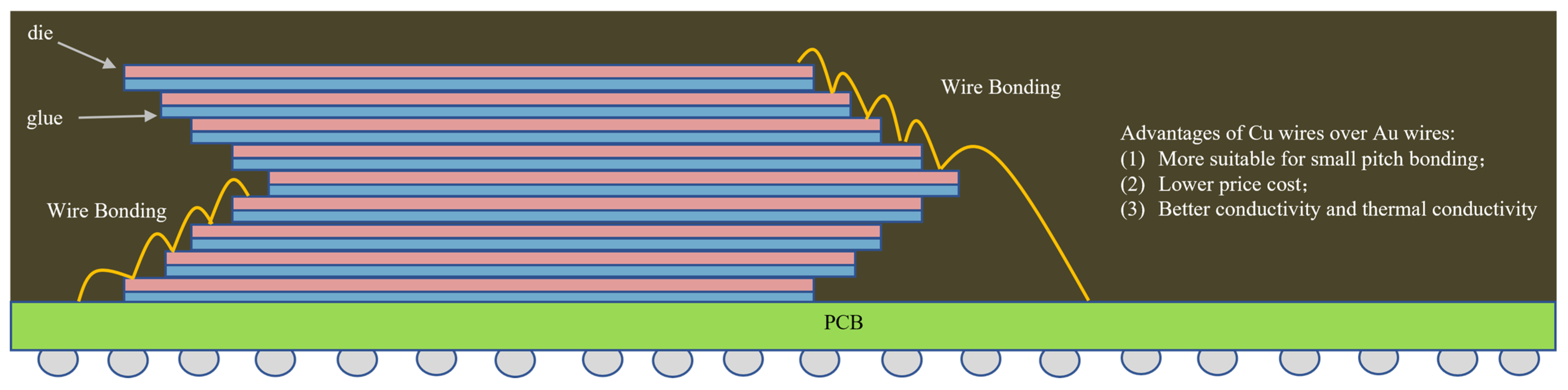
Figure 9.
Samsung’s memory chip stack.

Figure 10.
Die stacking using TSV technology.

Figure 11.
PoP structure: (a) WB (wire bonding); (b) flip–chip interconnection; (c) WB and flip–chip interconnection.
Figure 11.
PoP structure: (a) WB (wire bonding); (b) flip–chip interconnection; (c) WB and flip–chip interconnection.

Figure 12.
First-generation PoP stacked structures.

Figure 13.
Top-view and cross-sectional view of PoP chip (for mobile DRAM and application processor (A7)) inside an iPhone 5s.
Figure 13.
Top-view and cross-sectional view of PoP chip (for mobile DRAM and application processor (A7)) inside an iPhone 5s.

Figure 14.
PoP assembled using TMV technology.
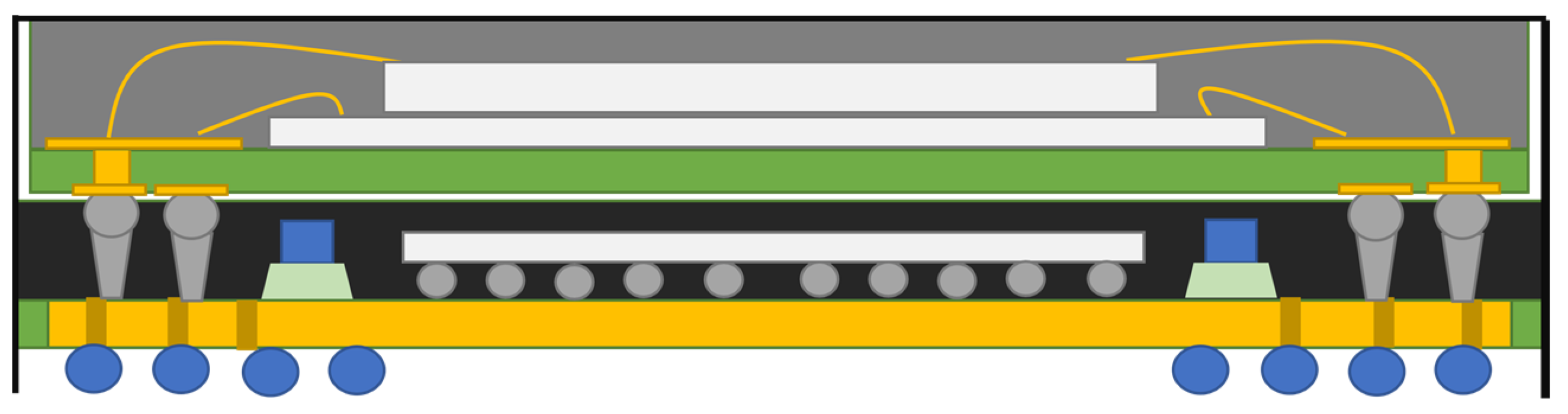
Figure 15.
TSMC/Apple’s PoP for their AP A12 with InFO-WLP.

Figure 16.
Manufacturing process: (a) TSOP stacking process; (b) flex stacking process.

Figure 17.
The manufacturing of a 3D memory package for a satellite: (a) stack of 6 QFPs with QFP I/Os; (b) stack of 4 BGAs with BGA I/Os; (c) stack of 4 SOPs with SOP I/Os.
Figure 17.
The manufacturing of a 3D memory package for a satellite: (a) stack of 6 QFPs with QFP I/Os; (b) stack of 4 BGAs with BGA I/Os; (c) stack of 4 SOPs with SOP I/Os.

Figure 18.
A 3D PLUS 3DSP21020 computer module (showing 11 integrated layers).

Figure 19.
A 128 K × 40 EEPROM device: (a) front morphology; (b) lateral morphology; (c) slice section in X direction; (d) slice section in Y direction.
Figure 19.
A 128 K × 40 EEPROM device: (a) front morphology; (b) lateral morphology; (c) slice section in X direction; (d) slice section in Y direction.

Figure 20.
A 128 K × 40 EEPROM device: (a) internal structure; (b) 5-layer stacking.

Figure 21.
NEO layer of Irvine sensors: (a) single die; (b) two dies.
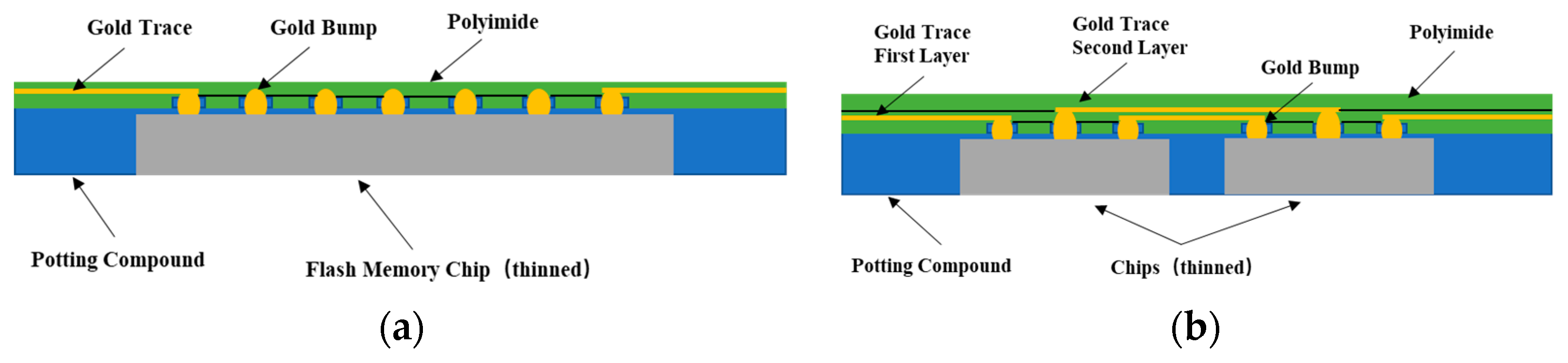
Figure 22.
Cube created from stack of NEO layers.

Figure 23.
Distribution of failure categories of electronic components.

Figure 24.
Experimental measurement device and characteristic parameters for the principle of moisture absorption of polymer materials.
Figure 24.
Experimental measurement device and characteristic parameters for the principle of moisture absorption of polymer materials.

Figure 25.
Finite element modeling flow for electronic components.

Figure 26.
Analysis flow of the combination of test analysis and finite element analysis.


Table 1.
ESA and CNES test plan (part).
| No. | Test Items | Test Method | Remarks |
|---|---|---|---|
| 1 | Thermal cycles under vacuum | 10−6 Torr 10 Cycles −40 °C/+70 °C, 2 °C/min, 1 h par palier | / |
| 2 | Electrical tests | Electrical tests at −55 °C/+25 °C/+125 °C | / |
| 3 | Thermal cycles | 500 cycles −55 °C/+125 °C 10 °C/mn, 15 mn par palier | External visual inspection and electrical tests −55 °C/+25 °C/+125 °C at 100, 300, and 500 cycles |
| 4 | Temperature and humidity under bias | 1000 h +85 °C and 85% RH | External visual inspection and electrical tests −55 °C/+25 °C/+125 °C at 240, 500, and 1000 h |
| 5 | Life test or high-temperature storage | 2000 h +125 °C | External visual inspection and electrical tests −55 °C/+25 °C/+125 °C at 500, 1000, and 2000 h |
| 6 | Power cycling | 30,000× ON/OFF 120 s ON (+110 °C) 60 s OFF (+40 °C) | External visual inspection and electrical tests −55 °C/+25 °C/+125 °C at 15 K and 30 K O/O cycles |
Table 2.
NASA GSFC Test Plan (part).
| No. | Test Items | Test Method | Remarks |
|---|---|---|---|
| 1 | Thermal conditioning | +125 °C, 48 h | / |
| 2 | Voltage conditioning | +125 °C, 320 h | / |
| 3 | Thermal characterization | 14 steps of 20 °C between −55 °C to 125 °C | / |
| 4 | Temperature and humidity under bias | 620 h +85 °C and 85% RH | C-SAM and X-ray |
| 5 | Mechanical shock | MIL-STD-883 Method 2002 200 G, 0.5 ms | / |
| 6 | Sine vibration | MIL-STD-202 Condition A 10 G to 22.5 G | / |
| 7 | Random vibration | MIL-STD-883 Method 2026 Condition E (16.4 G) Condition B (7.3 G) | / |
Table 3.
The typical failure modes of electronic components under environmental stress.
| Typical Environmental Stress | Test Item | Typical Failure Mode |
|---|---|---|
| Temperature stress | High temperature | Functional performance failure, material degradation. |
| Low temperature | Functional performance failure, material degradation. | |
| Thermal shock | Functional performance failure, mark shedding, shell coating fading, delamination. | |
| Temperature cycling | Functional performance failure, mark shedding, shell coating fading, delamination. | |
| Hygrothermal stress | Steady damp heat | Mark shedding, corrosion, functional performance failure, delamination, etc. |
| Pressure cooker | Mark shedding, pin breakage, internal filler precipitation, corrosion, functional performance failure, delamination, etc. | |
| Mechanical stress | Shock | Pin fracture or crack, ceramic body fracture or crack, cover plate leakage, glass insulator crack, bonding wire fracture or collapse, etc. |
| Vibration | Pin fracture, ceramic body fracture or crack, cover plate leakage, glass insulator crack, bonding wire fracture or collapse, etc. | |
| Constant acceleration | Functional performance failure, chip detachment, bonding wire lead detachment or collapse, cover plate leakage, shell fracture or cracking, etc. |
Table 4.
Thermal humidity correspondence relationship in moisture diffusion analysis.
| Characteristic | Heat Diffusion | Research Conclusion |
|---|---|---|
| Variable | Temperature | Relative humidity (W) |
| Conductivity | λ (W·m−1·K−1) | D·Csat (kg·s−1·m−1) |
| Specific heat capacity | c (J·kg−1·K−1) | Csat (kg·m−3) |
Table 5.
Typical reliability test items.
| Test Type | Test Items | Typical Conditions | Purpose |
|---|---|---|---|
| Thermal test | Temperature cycling | Method 1010 test condition C −65–+150 °C, Transfer time: 1 min, dwell time: 10 min | This test is conducted to determine the resistance of a component to high- and low-temperature extremes and the effect of alternate exposures to these extremes. |
| Thermal shock | Method 1011 test condition C −65–+150 °C, Transfer time: 10 s, dwell time: 2 min | The purpose of this test is to determine the resistance of the component to sudden exposure to extreme changes in temperature and the effect of alternate exposures to these extremes. | |
| Mechanical test | Random vibration | Method 2026 test condition E 20 (m/s2)2/Hz, 169.1 m/s2 | This test is conducted to determine the ability of the microcircuit to withstand the dynamic stress exerted by random vibration applied between upper and lower frequency limits in order to simulate the vibrations experienced in various service field environments. |
| Mechanical shock | Method 2002 test condition D 49,000 m/s2, 0.3 ms | The shock test is intended to determine the suitability of devices for use in electronic equipment. They may be subjected to moderately severe shocks as a result of suddenly applied forces or abrupt changes in motion caused by rough handling, transportation, or field operations. | |
| Humidity test | Moisture resistance | Method 1004 test 80–100% RH, 10 continuous cycles | The moisture resistance test is performed for the purpose of rapidly evaluating the resistance of component parts and constituent materials to the deteriorative effects of high-humidity and -heat conditions typical of tropical environments |
| Life test | Steady-state life | Method 1005 test condition B +125 °C, 1000 h | The steady-state life test is performed to demonstrate the quality or reliability of devices subjected to specific conditions over an extended time period. |
Table 6.
Summary of the main research on PoP packaging under thermal stress.
| Research Approach | Methods | Conclusions | References |
|---|---|---|---|
| Experiment, finite element simulation, model prediction | Temperature cycle test and Coffin–Manson model were used to evaluate the thermal fatigue reliability of solder joints. | The results indicate that the maximum accumulated inelastic hysteric energy in the fine-pitch ball grid array (FBGA) structure at the bottom of the product occurs on solder balls, and the two symmetric angles of the solder balls are prone to thermal fatigue and cracks, with thermal fatigue damage extending rapidly from the outer ball array to the inner ball array. By analyzing the failure data of solder balls, a thermal fatigue failure criterion was defined, where the critical failure probability value was approximately 80%. | Zhi-Hao Zhang [116] |
| Experiment, finite element simulation, model prediction | Thermal shock, the off-line coupling test of temperature cycle and thermal shock, as well as Knecht–Fox model were used to evaluate the reliability of solder joints. | The results indicate that both the top and bottom solder joints of PoP packaging show periodic changes in strain, with stress mainly concentrated on the solder joints and chips, and with solder joints being the most prone to failure. The maximum stress of the bottom chip is greater than that of the top chip, and the overall stress of the bottom solder joint is greater than that of the top solder joint. Moreover, the maximum stress of the bottom solder ball is located on the corner solder ball at the outermost corner of the solder ball array. | Wang Yang [117] |
| Experiment | Moiré interferometry was used to measure the warpage deformation of the ball grid array (BGA) in the upper and lower layers of PoP packaging devices during reflow welding. Moreover, the reliability of PoP packaging with different assembly processes under the same warpage condition was compared and analyzed via accelerated temperature cycling and four-point bending cycle tests. | The results indicate that the top-layer BGA of PoP packaging can have a high reliability whether dipped with flux or solder paste, whereas the bottom-layer BGA is significantly less reliable when dipped with solder paste in the four-point bending cycle test. | Wang Hongxia [118] |
| Experiment, finite element simulation, model prediction | Thermal shock test and Knecht–Fox model were used to evaluate the reliability of solder joints. | The results indicate that the stress of the entire packaging is concentrated on the internal chip and solder joints, with the maximum stress at the corner solder joints of the bottom solder ball array, which is the weak link of PoP packaging devices. Moreover, the stress of each row of solder balls shows a trend of gradually increasing from the center to the edge, and there is no significant difference between the stress of each row of balls at the top. The larger the size of the packaging chip, the lower the reliability of solder joints. | Xiusheng [119] |
| Finite element simulation | Finite element simulation was used to evaluate the reliability of solder joints under temperature cycling load. | The results indicate that the key solder ball is located in the solder balls in the diagonal corner of the bottom packaging. The reliability of solder joints can be improved by increasing the diameter and spacing of solder balls and reducing the thickness of the bottom packaging. In addition, the selection of an appropriate bottom filler and bonding material is also helpful for improving the reliability of solder joints. | Zhaohui Chen [120] |
Table 7.
Summary of main research on PoP packaging under hygrothermal stress.
| Research Approach | Methods | Conclusions | References |
|---|---|---|---|
| Finite element simulation | Finite element simulation was used to study the influence of moisture stress introduced by hygroscopic expansion and thermal stress introduced during reflow welding on the reliability of PoP packaging. | The results indicate that the maximum hygrothermal–mechanical stress occurs at the corners of the solder ball at the packaging edge, and the hygrothermal–mechanical stress of the top packaging chip is greater than that of the bottom packaging chip. The hygrothermal–mechanical stress of the outer solder ball is larger than that of the inner solder ball, and the hygrothermal–mechanical stress of the solder ball mainly occurs at the corners. | Liu Hailong [121] |
| Experiment, finite element simulation | High-temperature storage and damp heat test were used to evaluate the reliability of PoP packaging solder joints. | The results indicate that the hygrothermal stress at 85 °C/85% RH has no significant effect on the warpage of PoP packaging, but the thermal stress leads to a larger warpage of PoP packaging, with the increasing the thickness of IMC. | Liu Hailong [122] |
| Experiment, finite element simulation | Finite element simulation and a damp heat test were used to evaluate the reliability of the top, bottom, and entire PoP packaging. | The results indicate that the overall moisture absorption of PoP packaging is greater than the sum of two individual components, but the warping deformation is less than either of the two individual components. | A. Guedon-Gracia [123] |
| Experiment, finite element simulation | Damp heat, reflow welding, and temperature cycling tests were used to evaluate the reliability of the TMV structure. | The results indicate that the critical position is located at the outer edge of the electrocoppering solder pad under reflow temperature and hygrothermal load conditions. The strain energy release rate of delamination between the copper and molding compound interface depends on the coefficient of thermal expansion and the elastic modulus of the molding compound. With the increase in the CME of the molding compound, the strain energy release rate sharply increases. The strain energy release rate of the outer edge delamination of the electrocoppering pad sharply increases with the increase in the thickness of plated copper. Moreover, it can increase with the increase in the length of the copper plate under reflux load. When the delamination length is less than 10 μm at 150 °C, it increases with the increase in the delamination length and decreases with the increase in the thickness of the molding plastic. | Zhaohui Chen [124] |
Table 8.
Summary of main research on PoP packaging under mechanical stress.
| Research Approach | Methods | Conclusions | References |
|---|---|---|---|
| Experiment, finite element simulation | Random vibration test and finite element simulation were used to evaluate the reliability of PoP packaging devices subjected to dynamic stress. | The results indicate that the reliability of the bottom component of PoP packaging is significantly lower than that of the top component, and the outermost solder ball of the bottom component is the weak link in PoP packaging under a vibration load. | Xia Jiang [125] |
| Experiment, finite element simulation, model prediction | Sinusoidal vibration test and rain-flow counting method were used to evaluate the vibration fatigue characteristics and reliability of PoP packaging. | The results indicate that the dynamic response of PoP packaging shows a strong nonlinearity. Using the same cycle times, the higher the order of magnitude of input, the lower the reliability. | Bing Yang [126] |
| Experiment, finite element simulation | Random vibration test was used to evaluate the reliability of solder joints and then analyze the influence of PoP packaging size on reliability. | The results indicate that the maximum stress in the bottom package occurs at the corners of the outermost solder ball array, and the maximum stress in the top package occurs at the corners of the innermost solder ball array. The change in the heights of solder joints has a great impact on the stress of the bottom-package solder joint, whereas it has less of an influence on the stress of top-package solder joints. The stress of top-package solder joints significantly increases as the standoff increases and decreases with increasing diameter. The combination height of the molding compound and the bump in the top package is proportional to the maximum stress of the top package and inversely proportional to the maximum stress of the bottom package. | Tang Haili [127] |
| Experiment, finite element simulation | Temperature cycling test and thermal vibration test were used to evaluate the reliability of PoP packaging solder joints. | The results indicate that the stress changes in the solder joints show a synchronous and opposite trend with the change in temperature, and the stress at the solder joint decreases with the increase in holding time during the holding stage. Different conditions such as temperature, holding time, and temperature change rate can all have an impact on random vibration. When subjected to random vibration at high temperature, the maximum stress of the solder joint is greater than that at low temperatures, and the solder joint stress is transferred from the central part of the inner-ring solder joint to the outer-ring solder joint. | Liu Zhaoyun [128] |
| Experiment, finite element simulation | Finite element method was used to simulate the reliability of PoP packaging components with different structural sizes and materials under dynamic stress and drop impact load. | The results indicate that the maximum normal tensile stress of solder joints decreases with the increase in PCB damping and solder joint diameter. The maximum normal tensile stress of truncated spherical solder joint is greater than that of cylindrical solder joint. The maximum tensile stress of lead-free solder joints decreases with the increase in tin content, and the maximum tensile stress is greater than that of the tin–lead solder joint. | Fan Zerui [129] |
| Experiment, finite element simulation | Finite element method was used to simulate the dynamic response of PoP packaging components under drop impact load and then analyze the failure mechanism of solder joints. | The results indicate that the maximum normal tensile stress of key solder joints in PoP packaging components decreases with the increase in PCB damping and solder joint diameter. The maximum normal tensile stress of a truncated spherical solder joint is greater than that of a cylindrical solder joint. The maximum tensile stress of lead-free solder joints is greater than that of tin–lead solder joints, and for lead-free solder, the maximum tensile stress of corner solder joints decreases with the increase in tin content. | Yao Xiaohu [130] |
Table 9.
Summary of main research on CoC packaging under thermal stress.
| Research Approach | Methods | Conclusions | References |
|---|---|---|---|
| Experiment, finite element simulation, model prediction | Temperature cycle test, Taguchi method, and Arrenius high-acceleration model were used to evaluate the reliability of IMC solder joints and Sn3.9Ag0.6Cu solder joints. | The results indicate that the maximum stress–strain was observed in the second solder joint on the diagonal of the IMC solder joint array. For the Sn3.9Ag0.6Cu solder joint array, the corner solder joints show the maximum stress–strain values, and these areas are the locations of crack propagation. The stress–strain and fatigue life of solder joints are more sensitive to residence and temperature, especially high temperatures. Increasing temperature or residence time, or decreasing temperature, can reduce the stress–strain levels of solder joints and extend their fatigue life. | Liang Zhang [131] |
| Experiment, finite element simulation | The effect of high-temperature storage (HTS) on the stress in and around Cu TSVs in 3D stacked chips was studied using scanning white-beam X-ray microdiffraction. | The results indicate that high-temperature stress can reduce the bonding force of copper and silicon in TSV and accelerate the aging and reduce the reliability of TSV in the long term. | Tengfei Jiang [132] |
| Experiment, finite element simulation | Temperature cycling test and finite element simulation were used to study the reliability of the TSV structure. | The results indicate that the maximum thermal stress occurs not only at the nickel annular edge but also at the corners of pads. This may result in failure or delamination of TSV pads. The maximum Von Mises stress increases with the diameter ratio and pad diameter. Based on these results, this study helps to obtain a clear thermal stress distribution of the TSV array, and possible failure regions in the TSV structure are identified. | H.-Y. Tsai [133] |
| Finite element simulation | Finite element simulation was used to evaluate the influence of temperature cycling stress on the reliability of the TSV structure and interface. | The residual thermal stress largely occurs at the interface of the bottom TSV chip and PCB due to the mismatch of CTE. The stress in the outer corner of the TSV array is significantly higher than that in the center. The Cu/SAC305/Cu interconnect between the chips has very little influence on the maximum interfacial stress of the TSV structure, and the solder suffers from relatively low stress. On the other hand, the accumulated plastic strain of copper increases as the thermal cycle increases and ultimately reaches a static hardening state. The TSV device suffers a similar equivalent stress at high and low temperatures with different stress states; a large standoff height of Cu-Cu interconnects will help relieve stress in the device. | Hui-Hui Yuwen [134] |
| Finite element simulation | Finite element simulation was used to evaluate the reliability of ball bumps under temperature cycling load. | The results indicate that Von Mises plastic strain increases with the increase in the number of stacked chips. The metal bumps in lower layers have greater Von Mises plastic strain than upper layers on average. The bump outside has a greater general Von Mises plastic strain than that inside. The weak point of this stacking structure in a 3D chip lies in the metal bumps on the edge of the substrate. | Zhou Zhang [135] |
Table 10.
Summary of main research on CoC packaging under hygrothermal stress.
| Research Approach | Methods | Conclusions | References |
|---|---|---|---|
| Experiment, finite element simulation | Damp heat test and reflow welding test were used to evaluate the reliability of CoC packaging components. | The results indicate that, in a hygrothermal environment, moisture absorption between the substrate and bonding layers of each chip is much lower than that of the plastic packaging material, and the moisture absorption of the bottom bonding layer is higher than that of the top bonding layer. Moreover, the maximum hygrothermal stress and thermal stress in the reflow soldering test are both in the corners of the bottom chip, and their values are 1.3 times higher than those for pure thermal stress. | Tang Yu [136] |
| Finite element simulation | Finite element method was used to simulate the influence of moisture diffusion and hygrothermal stress on the reliability of CoC packaging devices. | The simulation results show that the bottom die-attach endured higher thermal stress conditions after moisture preconditioning under 85 ć/85% RH. In a simulation of hygroscopic swelling stress during the reflow process, it was indicated that the critical position for package reliability is located at the corner of the bottom die and the interface between the bottom die-attach and die. The reliability of the bottom layers is relatively low in a hygrothermal environment. | Wenmin Zhu [137] |
| Finite element simulation | Finite element method was used to simulate the influence of moisture diffusion and hygrothermal stress on the reliability of CoC packaging devices. | The results show that the substrate and bottom adhesive are rapidly absorbed during a moisture diffusion simulation. This reduces the mechanical properties of the stacked die, and this finding may provide a valid solution that can prevent the current failures observed in the industry. | Z K Hua [138] |
| Finite element simulation | Finite element method was used to simulate the influence of moisture diffusion and hygrothermal stress on the reliability of CoC packaging devices. | The results indicate that the influence of hydrothermal stress is greater than that of individual thermal stress, and the hydrothermal stress is about 1.3 times higher than thermal stress on average. The suspension area between the top chip and the spacer is a dangerous location for chip stress concentration, which is a unique phenomenon of CoC packaging. | Ye Anlin [139] |
| Finite element simulation | Finite element method was used to simulate the influence of moisture diffusion and hygrothermal stress on the reliability of CoC packaging devices. | The results indicate that the moisture desorption during the reflow welding process is faster than that in pretreatment. The maximum stress appears in the bottom chip and the bonding layer of chip interconnection. Hygroscopic expansion and internal vapor pressure can exert a significant impact on stress. Furthermore, the combined stress and warpage are far greater than a single stress factor. Under the combined effects of hygro-mechanical stress, thermal–mechanical stress, and vapor-pressure-induced stress, the strain energy release rate increases with temperature during reflow. | Jing Wang [140] |
Table 11.
Summary of main studies on the reliability of PiP packaging.
| Research Approach | Methods | Conclusions | References |
|---|---|---|---|
| Finite element simulation | Finite element method was used to simulate the reliability of solder joints under random vibration and temperature cycles. | The results indicate that the design of screw fixing points on printed circuit boards is key to improving the reliability of 3D-Plus memory board level assembly, and the reliability can be further improved using epoxy adhesive reinforcement. | Lv Qiang [141] |
| Finite element simulation | Finite element simulation and Anand model were used to evaluate the effects of tin–lead solder 63Sn37Pb and lead-free solder 95.5Sn3.8Ag0.7Cu on the reliability of 3D-Plus memory solder joints. | The results indicate that the solder joint stress and plastic strain show significant periodic changes. By comparing the two equivalent stress and plastic strain curves of lead-free solder and tin–lead solder, it can be found that the reliability of 95.5Sn3.8Ag0.7Cu solder is greater than that of 63Sn37Pb solder. | Nuo Bao [142] |
| Experiment, finite element simulation | Finite element simulation and thermal shock test were used to evaluate the reliability of solder joints. | The results indicate that the failure of solder joints is mainly caused by thermal fatigue, and the cracks are caused by the accumulation of plastic and creep strains. Crack initiation and propagation are mainly affected by the accumulation of inelastic strain, with the change trend affected by the difference in thermal expansion coefficients. | Zhou Shuai [143] |
| Experiment | Anti-radiation tests, such as total ionization dose (TID) and single-event effects (SEE), were used to evaluate the reliability of products for space applications. | The results indicate that the device can withstand a total ionizing dose of 100 Krad (Si) and a SEE of 60 MeV/mg·cm2, meeting the requirements of aerospace missions. | T.Dargines [144] |
| Experiment | Temperature, humidity, electrical stress, vibration, and impact tests were used to evaluate product reliability. | The results indicate that the device can function normally within the temperature range of −55–125 °C and withstand a high order of mechanical stress and thermal stress, much higher than industrial/commercial 3D packaging memory products, thus further proving the applicability of the product in the field of high reliability. | Jeannette Plante [53] |
Table 12.
Summary of main studies on the reliability of 3D packaging memory under multi-stress coupling.
Table 12.
Summary of main studies on the reliability of 3D packaging memory under multi-stress coupling.
| Research Approach | Methods | Conclusions | References |
|---|---|---|---|
| Finite element simulation | Finite element simulation and numerical analysis were used to discuss the influence of cracks and thermal–mechanical coupling loads on the reliability of TSV structure. | The results indicate that the crack propagation of the TSV structure is influenced by the coupling factors of material plasticity, crack length, location, direction, crack number, and load conditions. Thermal–mechanical coupling loads can significantly improve the capability of crack propagation. | Zhengwei Fan [145] |
| Finite element simulation | Finite element simulation was used to study the reliability of a 3D packaging CSP solder joint under thermal–vibration coupling loads. | The results indicate that the stress–strain distribution in solder joints is uneven, with the maximum stress–strain at the outermost corner of the solder joint array, and the stress–strain at the top solder joint is greater than that at the bottom solder joint. | LiShuai Han [146] |
| Finite element simulation | Finite element simulation was used to analyze the influence of electric–thermal coupling loads on the reliability of TSV structure. | The results indicate that there is a large current density and equivalent stress at the corner of the TSV/Micro-bumps interface, which easily leads to the failure of TSV structure. The electro-thermal–mechanical reliability of the TSV structure can be improved by increasing the diameter and decreasing the length of the through-holes. With the increase in SiO2 layer thickness, the maximum current density increases, and the maximum equivalent stress decreases. | YU Sijia [147] |
| Finite element simulation | Finite element simulation was used to analyze the influence of wet–thermal coupling loads on the reliability of 3D CoC packaging. | The results show that the most susceptible region for reliability risk impact in 3D chip-stacked packages is the interface between the solder ball, corresponding layer, and substrate. The hygrothermal coupling equivalent stresses near the solder ball edges are the most demanding in the package. | Tingting Zhao [148] |
Disclaimer/Publisher’s Note: The statements, opinions and data contained in all publications are solely those of the individual author(s) and contributor(s) and not of MDPI and/or the editor(s). MDPI and/or the editor(s) disclaim responsibility for any injury to people or property resulting from any ideas, methods, instructions or products referred to in the content. |
© 2023 by the authors. Licensee MDPI, Basel, Switzerland. This article is an open access article distributed under the terms and conditions of the Creative Commons Attribution (CC BY) license (https://creativecommons.org/licenses/by/4.0/).
Share and Cite
MDPI and ACS Style
Zhou, S.; Ma, K.; Wu, Y.; Liu, P.; Hu, X.; Nie, G.; Ren, Y.; Qiu, B.; Cai, N.; Xu, S.; et al. Survey of Reliability Research on 3D Packaged Memory. Electronics 2023, 12, 2709. https://doi.org/10.3390/electronics12122709
AMA Style
Zhou S, Ma K, Wu Y, Liu P, Hu X, Nie G, Ren Y, Qiu B, Cai N, Xu S, et al. Survey of Reliability Research on 3D Packaged Memory. Electronics. 2023; 12(12):2709. https://doi.org/10.3390/electronics12122709
Chicago/Turabian StyleZhou, Shuai, Kaixue Ma, Yugong Wu, Peng Liu, Xianghong Hu, Guojian Nie, Yan Ren, Baojun Qiu, Nian Cai, Shaoqiu Xu, and et al. 2023. "Survey of Reliability Research on 3D Packaged Memory" Electronics 12, no. 12: 2709. https://doi.org/10.3390/electronics12122709
Note that from the first issue of 2016, this journal uses article numbers instead of page numbers. See further details here.