


Experiment Study of Single Event Functional Interrupt in Analog-to-Digital Converters Using a Pulsed Laser


1
State Key Laboratory of Space Weather, National Space Science Center, Chinese Academy of Sciences, Beijing 100190, China
2
School of Electronic Electrical and Communication Engineering, University of Chinese Academy of Sciences, Beijing 100049, China
3
Chengdu Sino Microelectronics Technology, Chengdu 610000, China
*
Authors to whom correspondence should be addressed.
Electronics 2023, 12(13), 2774; https://doi.org/10.3390/electronics12132774
Submission received: 5 June 2023
/
Accepted: 21 June 2023
/
Published: 22 June 2023
(This article belongs to the Special Issue New Insights in Radiation-Tolerant Electronics)
Abstract
:Single Event Functional Interrupt (SEFI) poses a severe threat to the normal operation of spacecraft. This paper investigates SEFI in Analog-to-Digital Converters (ADCs) with storage units using precision positioning of pulsed lasers. Based on the experiment, it was discovered that a bit flip in the configuration registers in ADCs results in changes in parameters such as digital filter frequency, operating mode, and gain, leading to an upward or downward offset of ADC output codes. Similarly, a bit flip in the calibration registers also causes ADC output codes to shift upwards or downwards, or even output a value of zero. Furthermore, it was observed that SEFI phenomena can occur due to current latch-up in ADC input pins, causing the inability to read or write data in ADC storage units. This current latch-up can be resolved through power cycling or configuring the pins into a high-impedance state. This work highlights the significance of SEFI phenomena in ADCs, emphasizing the serious threat posed by storage unit flipping-induced SEFI to the proper functioning of ADCs. Moreover, the SEFI phenomenon caused by current latch-up in input pins is difficult to detect in practice, making it highly elusive. Once it occurs, it severely impacts the functionality of ADCs.
1. Introduction
SEFI is a multifaceted failure phenomenon that arises when high-energy particles collide with sensitive regions, such as control registers and circuits within devices, leading to abnormal operational states such as test mode activation, reset mode engagement, or temporary functional failures [1,2,3,4]. As technology progresses, integrated circuits are growing increasingly intricate, encompassing diverse storage units, control circuits, and other complex circuitry, making them more vulnerable to SEFI [5,6,7,8]. Within Synchronous Dynamic Random-Access Memory (SDRAM), the logical state of mode register flip-flops can induce SEFI, while flip-flops in the READ latch region can also contribute to SEFI, which can be rectified through software or power cycling [9,10]. Configuration Random-Access Memory (CRAM) storage units in Static Random-Access Memory (SRAM)-based Field Programmable Gate Arrays (FPGAs) are employed for user logic implementation, and the occurrence of a flip-flop anomaly in this area may lead to abnormal FPGA functionality with a certain probability [11,12,13]. Similarly, ADC devices encompass internal control registers or circuits, and high-energy particle impacts in these regions can trigger SEFI in ADCs, posing a significant threat to their reliability [14]. However, compared to other devices, SEFI research concerning ADCs has received limited attention, with existing studies primarily focusing on evaluating the SEFI cross-section of ADCs [15,16,17].
As technology continues to advance, an increasing number of ADC devices are equipped with storage units to store calibration information, configure operating modes, adjust digital filter cut-off frequencies, and modify gain sizes [18]. Scheick et al. observed various SEFI phenomena caused by flips in the ADC configuration registers through heavy ion experiments. These included changes in the ADC’s sampling polarity, entering Power Down mode, and alterations in the signal gain settings [14]. Pulsed lasers offer advantages such as ease of operation, wide and continuously adjustable energy range, precise positioning, and low cost. Due to these unique advantages, they provide an opportunity for detailed investigation of the SEFI mechanism in electronic devices. Bougerol et al. utilized the advantage of high-precision positioning of a pulsed laser to conduct SEFI research on SDRAM memory [19]. A pulsed laser can serve as a complementary tool to systematically unveil all potential radiation effects and their corresponding locations. The precision of laser irradiation allows for the accurate triggering of single event effects, thereby enabling the reproduction of all observed heavy ion events, including single-bit upsets, multiple-bit upsets, fuse-latch upset, and large errors [19].
To investigate the SEFI phenomenon of ADCs in more detail, this study utilized the high-precision point-by-point scanning technique of a pulsed laser to scan the active region of an ADC with storage units. The sensitive areas of Single-Event Upset (SEU) and SEFI within the ADC were identified, and the impact of SEU on ADC functionality was observed for individual configuration and calibration registers. The experimental results show the impact of a bit flip in the configuration and calibration registers at different positions on the conversion function of the ADC. Furthermore, a new SEFI phenomenon caused by the abnormal current of the “RFS” pin of the ADC is discovered in the experiment. The analysis of this phenomenon is presented, and some protective measures are proposed to avoid this type of SEFI.
This article is organized as follows: Section 2 introduces the pulse laser’s experimental setup and the ADC’s SEFI test method. Next, Section 3 discusses the specific impact of the configuration register and calibration register to flip on ADC output. The phenomenon of no data output from ADC caused by an increase in pin current is described. In Section 4, corresponding protection measures are proposed based on the mechanisms of SEFI generation. Finally, the conclusions are presented in Section 5.
2. Experimental Devices and Methods
2.1. Experimental Setup
This paper uses the PPLSEE-1 pulsed laser experimental device to simulate Single-Event Effects (SEE) through pulsed laser irradiation. The technical specifications of the PPLSEE-1 are shown in Table 1. PPLSEE-1 achieves precise positioning of SEFI-sensitive areas through controlling the movement of the Device Under Test (DUT) through a high-precision three-dimensional moving platform [20,21,22].
We have developed a testing system for investigating the SEFI of ADCs, which is illustrated in Figure 1. The testing system comprises an FPGA-based mainboard, a PCI Extension for Instrumentation (PXI) system, and a DUT sub-board. The mainboard is connected to the sub-board, providing power and real-time monitoring to the DUT sub-board. It can also control the functions of the DUT and read data from the DUT’s output register, configuration register, and calibration register. The PXI system sends control instructions to the mainboard and receives test data from the mainboard through an RS422 serial port. The signal generator in the PXI system provides the ADC with analog signal input, while the DC power supply and digital multimeter provide power to the mainboard and real-time monitoring.
2.2. DUT
The ADC device under testing is AD7710, manufactured by Analog Devices, which adopts the ∑-Δ algorithm and has a dual-channel sampling capability. The AD7710 employs a 0.6 μm dielectric isolation Bipolar CMOS process for its fabrication. The chip also has a differential input mode, an analog voltage input range of −2.5 V to 2.5 V, and is packaged in a Small Outline Integrated Circuit (SOIC) package (SOIC). It supports self-calibration, system calibration, background calibration, and other modes. The internal structure of AD7710 is shown in Figure 2, which includes a 24-bit output register, a 24-bit configuration register, and a 24-bit calibration register, and these registers are sensitive to SEU. The output register is used to store the data converted by the ADC, the calibration register is used to store the calibration data when the ADC is initialized, and the configuration register is used to save the ADC configuration information. Through writing to the configuration register, the sampling channel selection, gain setting, signal polarity selection, and other functions can be achieved. Before the pulse laser test, the AD7710 chip is subjected to a backside package opening treatment to expose the backside silicon substrate.
2.3. Experimental Method
The DUT sub-board is first fixed to the three-dimensional moving platform when conducting the ADC pulse laser test. The platform is controlled to move the chip to the specified starting point, and the Z-axis of the moving platform is adjusted to focus the laser on the active area of the chip’s backside. Next, the energy of the pulsed laser is 1500 pJ. The laser frequency is set to 1 kHz, and the speed of the three-dimensional moving platform is set to 5 mm/s. Finally, the mainboard is powered on, and the PXI system sends test instructions to the mainboard and provides a sine wave input signal to the ADC device. The analog input sine wave of the ADC has a frequency of 2 Hz, an amplitude of 2.5 V, and a center offset of 1.25 V. The PXI system records and displays the ADC’s power current and output data while the laser scanner scans the active area. The digital power supply voltage and analog power supply voltage of AD7710 are both 5 V. The setup of a pulsed laser simulation of the SEFI experiment for the ADC is shown in Figure 3.
Method for SEFI testing of configuration register: First, the main board writes the initialization data of number 1 in Table 2 to the configuration register of the ADC. After waiting for the ADC’s self-calibration to complete, the entire active area is scanned with a laser, and the main board continuously reads the configuration register. Then, the areas that cause a flip in the configuration register are identified as sensitive regions for the configuration register. Finally, the sensitive region of the configuration register is scanned point by point using pulsed lasers, and the data from the output register and configuration register are cyclically read to observe the impact of a bit flip in the configuration register on the output of the ADC.
Calibration registers SEFI test method: The calibration registers of the ADC include four types: zero-scale calibration registers (ZSCR) and full-scale calibration registers (FSCR) for channel 1, and ZSCR and FSCR registers for channel 2. We selected the ZSCR and FSCR for channel 2. The mainboard writes the data number 2 in Table 2 to the ADC’s configuration register [18]. After the ADC enters the read/write mode of the ZSCR register, the mainboard writes the data number 4 in Table 2 to the ZSCR to avoid the influence of the coefficient change caused by each self-calibration on the test results. After the calibration coefficients are written, the remaining operations are similar to the test method of the configuration register, observing the effect of a bit flip in the calibration register on the output of the ADC.
3. Results and Discussion
Figure 4a shows the cross-section of the output register flip-flop obtained via scanning the areas outside the configuration register and calibration register regions. The configuration register flip-flop cross-section was obtained via scanning the configuration register region, as shown in Figure 4b. The formula for calculating the flip-flop cross-section of the register [23] is given as follows:
where represents the number of flip-flop occurrences; represents the irradiation scanning area of the DUT; represents the frequency of the pulsed laser; represents the scanning time of the pulsed laser. At an energy of 300 pJ, no flip occurred in the configuration register, while the flip cross-section reached saturation at 1000 pJ. From Figure 4, it can be clearly observed that the flip cross-section of the configuration register is two orders of magnitude higher than that of the output register. This is because, during normal operation of the ADC, the output register receives new converted data at regular intervals, which overwrite the previously flipped data. However, in the experiment, the configuration register data are not overwritten with new configuration data. As a result, the flip cross-section of the output register is lower than that of the configuration register.
3.1. SEFI Caused by Configuration Register Flipping
Flipping different positions in the AD7710 configuration register has various impacts on the ADC’s functionality. The functions of each bit in the AD7710 and their effects on the ADC output after flipping are shown in Table 3.
When a bit flip occurs in bits 0 to 11 of the configuration register, parameters such as the first notch frequency, cutoff frequency, and output data rate of the digital filter are affected. It primarily causes an upward or downward offset in the converted code values of the ADC. As illustrated in Figure 5a, when the third bit of the configuration register flips, it results in a downward offset of 0.847 V in the ADC output data. Figure 5b illustrates the impact of a bit flip in bits 0 to 11 of the configuration register on the offset of the ADC output. The X-axis represents bits 0 to 11 of the configuration register, while the Y-axis represents the offset in the ADC output code values resulting from the register flipping. To facilitate a more intuitive observation of the difference between the ADC output code values and the sampled signals, the 24-bit code values are converted to voltage values ranging from 0 to 2.5 V. From Figure 5b, it can be observed that flipping either the lower or higher bits of the configuration register leads to significant offsets in the ADC output code values, with the offset reaching a maximum of 2.5 V. This implies that the ADC output data approaches zero, posing a serious threat to the proper functioning of the ADC. Although the flipping of the third bit of the configuration register results in a first trap frequency and a cutoff frequency much higher than the input signal frequency, significant offsets in the ADC output code values still occur, drawing our attention.
The output data rate of AD7710 is related to the decimation ratio of the digital filter, and as the decimation ratio changes, the gain of the digital filter also varies. The ZSCR zeroes the offset from the input circuit to the digital filter, while the FSCR is used to calibrate the full-scale change caused by a change in the decimation ratio. Therefore, when the parameters of the digital filter change, it is necessary to recalibrate the ADC so that the digital filter parameters match the calibration parameters, in order to eliminate offset errors and gain errors.
In Figure 6a, flipping configuration register 12 from 1 to 0 switches the ADC’s sampling signal input from unipolar to bipolar, leading to an upward shift of the ADC’s output signal by 1.25 V. In the unipolar input mode, the voltage input range between AIN2(−) and AIN2(+) is 0 V to 2.5 V, while in bipolar mode, the input range extends from −2.5 V to 2.5 V, resulting in a halving of the code value of the output data. Flipping configuration register 13 activates the Burn-Out Current, which detects the presence of the sampling resistor in the circuit but has no impact on the signal output. Flipping configuration register 14 turns on the Output Compensation Current, a feature that is unused in the experimental circuit and hence has no effect on the signal output. Flipping configuration register 15 from 1 to 0 reduces the word length of the ADC output data from 24 bits to 12 bits, with no significant changes in the output code values observed during the experiment. When configuration register 16 is flipped, the ADC enters the “Power-down” mode, with a resultant change in the ADC’s power supply current, as shown in Figure 6b. The analog power supply is switched off, and the digital power supply current is reduced, leading to no data output from the ADC. Flipping configuration register 17 changes the sampled channel, which alters the output data.
In Figure 7a, the configuration register bit 19 changed from 0 to 1, causing the ADC gain to change from one to four. As a result, the output signal curve shifted upwards, and multiple output signals reached the full range of 2.5 V. In Figure 7b, the 22nd bit is flipped, causing the ADC to enter the system calibration mode from normal mode. However, upon entering the system calibration mode, due to the absence of accurate calibration voltage provided to the VIN input of the ADC, the calibration process fails, resulting in abnormal output data.
3.2. SEFI Caused by Calibration Register Flipping
According to Figure 8, a bit flip of the calibration register has an impact on the ADC output. The X-axis in the figure represents the storage bits of the calibration register from 0 to 23, while the Y-axis represents the offset of the ADC output after the calibration register flipping. The red dots indicate the offset of the ADC output when a bit flip occurs in the FSCR, while the gray squares represent the offset when a bit flip occurs in the ZSCR. From the figure, it can be observed that the flipping of the calibration registers in bits 0 to 16 has a minimal impact on the ADC output. However, starting from bit 17, the influence of the calibration register flipping on the ADC output gradually increases with the increasing number of bits. When the 22nd bit of the zero-scale calibration register flips, the ADC output offset reaches its maximum value of 2.5 V, causing the ADC output to be zero. On the other hand, when the 22nd bit of the full-scale calibration register flips, the ADC output offset is approximately 1.57 V.
The data stored in the FSCR and ZSCR directly influence the gain and offset of the ADC. When changes occur in the data of the FSCR or ZSCR, the corresponding calibration parameters are also altered. This causes the ADC to utilize incorrect gain and offset values in subsequent conversion processes, leading to a shift in the output code values. For example, an increase in the value of the FSCR amplifies the ADC’s gain, resulting in an increased amplitude of the output code values relative to the input signals, generating a positive shift. Similarly, variations in the ZSCR also induce shifts. Therefore, to ensure the accuracy of the ADC, recalibration is necessary when the data in the FSCR and ZSCR undergo changes. This recalibration process involves readjusting the gain and offset of the ADC to match the new calibration parameters, thereby eliminating the offset in the output code values.
3.3. SEFI Caused by Pin Current Latch-Up
In the pulse laser experiment of the ADC, we gradually increased the energy of the pulse laser from 200 pJ to 3 nJ and performed a comprehensive scan of the entire active region. Surprisingly, throughout all the scans, we did not observe Single-Event Latch-up (SEL) in the analog and digital power supplies of the ADC. However, when scanning specific areas, we noticed a 12 mA increase in the mainboard power supply, accompanied by the ADC ceasing to output data. After power cycling the ADC, it returned to normal operation. This phenomenon caught our attention. Through simultaneously monitoring the analog power supply, digital power supply, and mainboard power supply of the ADC, we found that the ADC power remained stable when the mainboard current increased by 12 mA. Additionally, besides the power connections, there are connections between the mainboard FPGA’s GPIO pins and the ADC, including SCLK, A0, TFS, and RFS pins.
To determine whether the SEFI phenomenon was caused by the abnormal current in the ADC pins, the following measures were taken: The FPGA was reconfigured to set the GPIO pins connected to the ADC to a high-impedance state, where the GPIO pins do not output any current externally. During the FPGA configuration process, there was a significant fluctuation in the mainboard power supply current. After the configuration was completed, the mainboard current returned to normal, ensuring no impact on the experimental results. During the experiment, the FPGA executed a program to read the ADC output registers to observe the effect of abnormal current on ADC functionality. Continuous power supply to the ADC was maintained throughout the experiment to avoid any disruption caused by power cycling the ADC.
Figure 9 illustrates the abnormal mainboard current caused by abnormal current in the ADC pins. It can be observed that after the pulsed laser irradiates the sensitive point, the mainboard current rapidly increases by approximately 12 mA and remains stable. After the current increases to 12 mA, it no longer increases because the GPIO driving capability of the FPGA is 12 mA. Even after the laser stops irradiation, the current does not return to normal. When the FPGA begins reconfiguration, the current increases by approximately 30 mA, and after the configuration is completed, it rapidly decreases to around 250 mA. In Figure 9a, when A0, SLK, or TFS pins are configured as high impedance, it can be observed that the mainboard power supply current does not return to normal after reconfiguration. However, in Figure 9b, when the RFS pin is configured as high impedance, the current immediately returns to normal. In conclusion, we can deduce that the abnormal current in the ADC is associated with the RFS pin. When there is abnormal current in the RFS pin, it is not possible to read the configuration and output registers of the ADC, and even after rewriting the ADC configuration registers, normal functionality cannot be restored.
Figure 10 illustrates the distribution of abnormal current points in AD7710. The graph depicts two different types of points: Red points indicate current abnormalities that can only be rectified through power cycling or configuring the RFS pin in a high impedance state. The yellow points represent the recoverable points for abnormal pin current. When the laser stops illuminating these sensitive points or when the laser illuminates the vicinity of these sensitive points, both the pin current and ADC functionality will return to normal. The green points signify intermittent “FFFFFF” error data output from the ADC, which resumes normal operation after laser irradiation stops. During occurrences of these current abnormalities, the ADC power supply current remains normal, but the RFS pin current exhibits abnormalities, resulting in abnormal ADC functionality and no data output. The red box represents the configuration register area, while the blue box represents the calibration register area.
The RFS pin is primarily used to control the data of the read configuration register, calibration register, and output register. When the pulsed laser irradiates the current anomaly point in Figure 11, a transient current is generated in the RFS circuit. As shown in Figure 11, when the RFS circuit is subjected to current perturbation , it causes Q1 to be in a forward-biased state. According to the equivalent circuit, it can be inferred that:
The currents flowing through Rs and Rw are denoted as and , respectively. Due to their relatively small magnitudes, they can be neglected. In this case, , where and are the gain coefficients of Q1 and Q2, respectively. When , a positive feedback loop is formed, resulting in a large current that leads to latch-up. Based on the latch-up equivalent model, the latch-up process can be divided into triggering and sustaining phases. The triggering phase occurs when the transient photocurrent and the gain coefficients and of the devices satisfy the triggering conditions for latch-up, leading to the activation of the latch-up path and the formation of positive feedback. The sustaining phase occurs when the voltage at the external input pin RFS of the device exceeds the latch-up sustaining voltage, allowing the positive feedback to generate a large current and maintain a continuous state of high current throughout the circuit. The triggering current only serves the purpose of initially triggering the conduction and does not affect the latch-up current of the final circuit.
The recovery mechanism of current at the recoverable current point in Figure 10 can be categorized into two situations. Firstly, when the pulsed laser irradiates the recoverable current point, the RFS circuit undergoes latch-up. Subsequently, when the pulsed laser irradiates near the vicinity of the abnormal point, it may trigger multiple latch-up paths, resulting in a competition for current among these paths. However, since none of the paths can satisfy the requirements for sustaining current, the RFS circuit eventually exits the latch-up state [24,25,26]. Secondly, for the sensitive points where the latch-up current returns to normal after the laser stops irradiation, a higher sustaining current is required compared to the unrecoverable current points. Consequently, when the laser ceases irradiation, the latch-up paths cannot meet the requirements for sustaining current, causing the RFS circuit to exit the latch-up state.
4. SEFI Protection
When the configuration and calibration registers of an ADC flip, the output code value may be offset or even become zero. In space applications, a typical working amplitude range for the input signal should be set for the ADC. Suppose the output data amplitude deviation exceeds the specified range due to configuration or calibration registers flipping. In that case, the configuration registers should be rewritten, and the ADC recalibrated to restore regular operation. In addition, through reading the flipped calibration and configuration register data, the abnormal data can be partially recovered via comparing the changes before and after the flip.
For the protection of RFS pin current anomalies, similar protective measures to SEL can be taken, such as restoring normal operation through power cycling or adding limiting resistors in the signal path [27,28,29]. In addition, in the process of reading ADC data, the RFS pin can be configured in a high-impedance state or a low level for a certain period of time after each reading is completed, and then the program can be reconfigured to restore normal operation.
5. Conclusions
This paper investigates the SEFI effects on ADC caused by configuration and calibration register flips induced by a pulsed laser. Bit flips of bits 0 to 11 in the configuration register result in a mismatch between the parameters of the digital filter and the calibration parameters of the calibration register, causing the output signal to shift upward or downward. Bit flips in bits 12 to 23 of the configuration register alter the operating mode, gain, and input signal polarity of the ADC, leading to an offset in the output code. Flip-flops in the calibration register change the maximum input range or zero offset deviation of the ADC, and specifically, flips in bits 17 to 23 can cause severe output offset or even output a value of zero. Therefore, the occurrence of bit flips in the configuration register and calibration register can be detected through monitoring the output code of the ADC, and normal operation can be restored by means of reconfiguring or recalibrating the affected registers. Furthermore, the AD7710 pin current latch-up phenomenon occurs when the parasitic PNPN structure in the RFS pin circuit becomes conducting, resulting in a short circuit between the RFS circuit and ground, thereby causing the failure of ADC register read/write functionality. The pin current latch-up can exit the latch-up state either due to the inability to sustain the required latch-up holding current or the triggering of multiple latch-up paths, leading to the restoration of normal ADC functionality. These findings provide valuable insights for the design and operation of spacecraft ADCs in mitigating SEFI-related risks and ensuring reliable performance.
Author Contributions
Conceptualization, Z.M. and X.Z.; methodology, X.Z. and Z.M.; software, Z.M.; validation, Z.M., X.Z., and H.L.; formal analysis, Z.M. and X.Z; investigation, Z.M.; resources, T.H. and X.Z.; data curation, Z.M.; writing—original draft preparation, Z.M.; writing—review and editing, Z.M., X.Z., and H.L.; visualization, Z.M.; supervision, J.H., X.Z., and H.L.; project administration, J.H., X.Z., and H.L.; funding acquisition, X.Z. All authors have read and agreed to the published version of the manuscript.
Funding
This research was funded by the Technical Basic Research Project (No. JSHS2019203B001).
Data Availability Statement
The data used to support the findings of this study are available from the corresponding author upon request.
Acknowledgments
This work was supported by the Effects Centre of State Key Laboratory of Space Weather of the National Space Science Center and research group members. The authors offer deep appreciation for their kind support.
Conflicts of Interest
The authors declare no conflict of interest.
References
- Koga, R.; Penzin, S.H.; Crawford, K.B.; Crain, W.R. Single event functional interrupt (SEFI) sensitivity in microcircuits. In Proceedings of the 4th European Conference on Radiation and Its Effects on Components and Systems (RADECS 97), Cannes, France, 15–19 September 1997; pp. 311–318. [Google Scholar]
- Ju, A.A.; Guo, H.X.; Ding, L.L.; Zhang, F.Q.; Zhong, X.L.; Pan, X.Y.; Zhang, H.; Bi, J.S. Analysis of Ion-Induced SEFI and SEL Phenomena in 90 nm NOR Flash Memory. IEEE Trans. Nucl. Sci. 2021, 68, 2508–2515. [Google Scholar] [CrossRef]
- Yang, W.; Li, Y.; Li, Y.; Hu, Z.; Xie, F.; He, C.; Wang, S.; Zhou, B.; He, H.; Khan, W.; et al. Atmospheric neutron single event effect test on Xilinx 28 nm system on chip at CSNS-BL09. Microelectron. Reliab. 2019, 99, 119–124. [Google Scholar] [CrossRef]
- Bagatin, M.; Gerardin, S.; Cellere, G.; Paccagnella, A.; Visconti, A.; Beltrami, S.; Harboe-Sorensen, R.; Virtanen, A. Key Contributions to the Cross Section of NAND Flash Memories Irradiated With Heavy Ions. IEEE Trans. Nucl. Sci. 2008, 55, 3302–3308. [Google Scholar] [CrossRef]
- Nekrasov, P.V.; Karakozov, A.B.; Bobrovskyi, D.V.; Marfin, V.A. Investigation of single event functional interrupts in microcontoller with PIC17 architecture. In Proceedings of the 2015 15th European Conference on Radiation and Its Effects on Components and Systems (RADECS), Moscow, Russia, 14–18 September 2015; pp. 1–4. [Google Scholar]
- Chen, D.; Wilcox, E.; Berg, M.; Kim, H.; Phan, A.; Figueiredo, M.; Seidleck, C.; LaBel, K. Single-event effect performance of a conductive-bridge memory EEPROM. IEEE Trans. Nucl. Sci. 2015, 62, 2703–2708. [Google Scholar] [CrossRef] [Green Version]
- Sánchez-Macián, A.; Reviriego, P.; Tabero, J.; Regadío, A.; Maestro, J.A. SEFI protection for nanosat 16-bit chip onboard computer memories. IEEE Trans. Device 2017, 17, 698–707. [Google Scholar] [CrossRef]
- Aranda, L.A.; Sánchez-Macián, A.; Maestro, J.A. A Methodology to Analyze the Fault Tolerance of Demosaicking Methods against Memory Single Event Functional Interrupts (SEFIs). Electronics 2020, 9, 1619. [Google Scholar] [CrossRef]
- Koga, R.; Yu, P.; Crain, S.; George, J. Proton and heavy ion induced semi-permanent upsets in double data rate SDRAMs. In Proceedings of the 2007 IEEE Radiation Effects Data Workshop, Honolulu, HI, USA, 23–27 July 2007; pp. 199–203. [Google Scholar]
- Guertin, S.M.; Patterson, J.D.; Nguyen, D.N. Dynamic SDRAM SEFI detection and recovery test results. In Proceedings of the 2004 IEEE Radiation Effects Data Workshop (IEEE Cat. No. 04TH8774), Atlanta, GA, USA, 22 July 2004; pp. 62–67. [Google Scholar]
- Tanaka, T.; Liao, W.; Hashimoto, M.; Mitsuyama, Y. Impact of Neutron-Induced SEU in FPGA CRAM on Image-Based Lane Tracking for Autonomous Driving: From Bit Upset to SEFI and Erroneous Behavior. IEEE Trans. Nucl. Sci. 2022, 69, 35–42. [Google Scholar] [CrossRef]
- George, J.; Koga, R.; Swift, G.; Allen, G.; Carmichael, C.; Tseng, C. Single event upsets in Xilinx Virtex-4 FPGA devices. In Proceedings of the 2006 IEEE Radiation Effects Data Workshop, Ponte Vedra Beach, FL, USA, 17–21 July 2006; pp. 109–114. [Google Scholar]
- Xiong, X.; Du, X.; Zheng, B.; Chen, Z.; Jiang, W.; He, S.; Zhu, Y. Soft Error Sensitivity Analysis Based on 40 nm SRAM-Based FPGA. Electronics 2022, 11, 3844. [Google Scholar] [CrossRef]
- Scheick, L.Z.; Allen, G.R.; Edmonds, L.D. Single-Event Effect Qualification of 24 Bit Analog-to-Digital Converters. In Proceedings of the 50th Annual IEEE Nuclear and Space Radiation Effects Conference (NSREC)/IEEE Radiation Effects Data Workshop (REDW), San Francisco, CA, USA, 8–12 July 2013. [Google Scholar]
- Esteban, A.; Bogorad, A.; Likar, J.; Moyer, S.; Herschitz, R. Single Event Effects on New High Speed Analog to Digital Converters, Digital to Analog Converters, Hybrid MUXDAC Devices, and Voltage Converters. In Proceedings of the 2006 IEEE Radiation Effects Data Workshop, Ponte Vedra Beach, FL, USA, 17–21 July 2006; pp. 43–49. [Google Scholar]
- Chen, K.; Chen, H.; Kierstead, J.; Takai, H.; Rescia, S.; Hu, X.; Xu, H.; Mead, J.; Lanni, F.; Minelli, M. Evaluation of commercial ADC radiation tolerance for accelerator experiments. J. Instrum. 2015, 10, P08009. [Google Scholar] [CrossRef] [Green Version]
- Kruckmeyer, K.; Trinh, T. Single event effects characterization of Texas Instruments ADC12D1600CCMLS, 12 bit, 3.2 GSPS analog-to-digital converter with static and dynamic inputs. In Proceedings of the 2014 IEEE Radiation Effects Data Workshop (REDW), Paris, France, 14–18 July 2014; pp. 1–7. [Google Scholar]
- Analog Devices Inc. AD7710 Datasheet. Available online: https://www.analog.com/media/en/technical-documentation/data-sheets/AD7710.pdf (accessed on 1 June 2023).
- Bougerol, A.; Miller, F.; Guibbaud, N.; Gaillard, R.; Moliere, F.; Buard, N. Use of Laser to Explain Heavy Ion Induced SEFIs in SDRAMs. IEEE Trans. Nucl. Sci. 2010, 57, 272–278. [Google Scholar] [CrossRef]
- Li, S.; Han, J.W.; Chen, R.; Shangguan, S.P.; Ma, Y.Q.; Wang, X. Study on the single-event upset sensitivity of 65-nm CMOS sequential logic circuit. Ieice Electron. Express 2020, 17. [Google Scholar] [CrossRef] [Green Version]
- Xin, J.; Zhu, X.; Ma, Y.; Han, J. Study of Single Event Latch-Up Hardness for CMOS Devices with a Resistor in Front of DC-DC Converter. Electronics 2023, 12, 550. [Google Scholar] [CrossRef]
- Feng, G.; Shangguan, S.; Ma, Y.; Han, J. SEE characteristics of small feature size devices by using laser backside testing. J. Semicond. 2012, 33, 014008. [Google Scholar] [CrossRef]
- Darracq, F.; Lapuyade, H.; Buard, N.; Mounsi, F.; Foucher, B.; Fouillat, P.; Calvet, M.-C.; Dufayel, R. Backside SEU laser testing for commercial off-the-shelf SRAMs. IEEE Trans. Nucl. Sci. 2002, 49, 2977–2983. [Google Scholar] [CrossRef]
- Johnston, A.; Baze, M. Mechanisms for the latchup window effect in integrated circuits. IEEE Trans. Nucl. Sci. 1985, 32, 4017–4025. [Google Scholar] [CrossRef]
- Plaag, R.; Baze, M.; Johnston, A. A distributed model for radiation-induced latchup. IEEE Trans. Nucl. Sci. 1988, 35, 1563–1569. [Google Scholar] [CrossRef]
- Johnston, A. The influence of VLSI technology evolution on radiation-induced latchup in space systems. IEEE Trans. Nucl. Sci. 1996, 43, 505–521. [Google Scholar] [CrossRef]
- Becker, H.N.; Miyahira, T.F.; Johnston, A.H. Latent damage in CMOS devices from single-event latchup. IEEE Trans. Nucl. Sci. 2002, 49, 3009–3015. [Google Scholar] [CrossRef] [Green Version]
- Jeong, S.-H.; Lee, N.-H.; Cho, S.-I. A Design of High-speed Power-off Circuit and Analysis. Trans. Korean Inst. Electr. Eng. 2014, 63, 490–494. [Google Scholar] [CrossRef] [Green Version]
- Andjelković, M.S.; Petrović, V.; Stamenković, Z.; Ristić, G.S.; Jovanović, G.S. Circuit-level simulation of the single event transients in an on-chip single event latchup protection switch. J. Electron. Test. 2015, 31, 275–289. [Google Scholar] [CrossRef]
Figure 1.
Schematic diagram of the test system.

Figure 2.
The internal structure of AD7710.
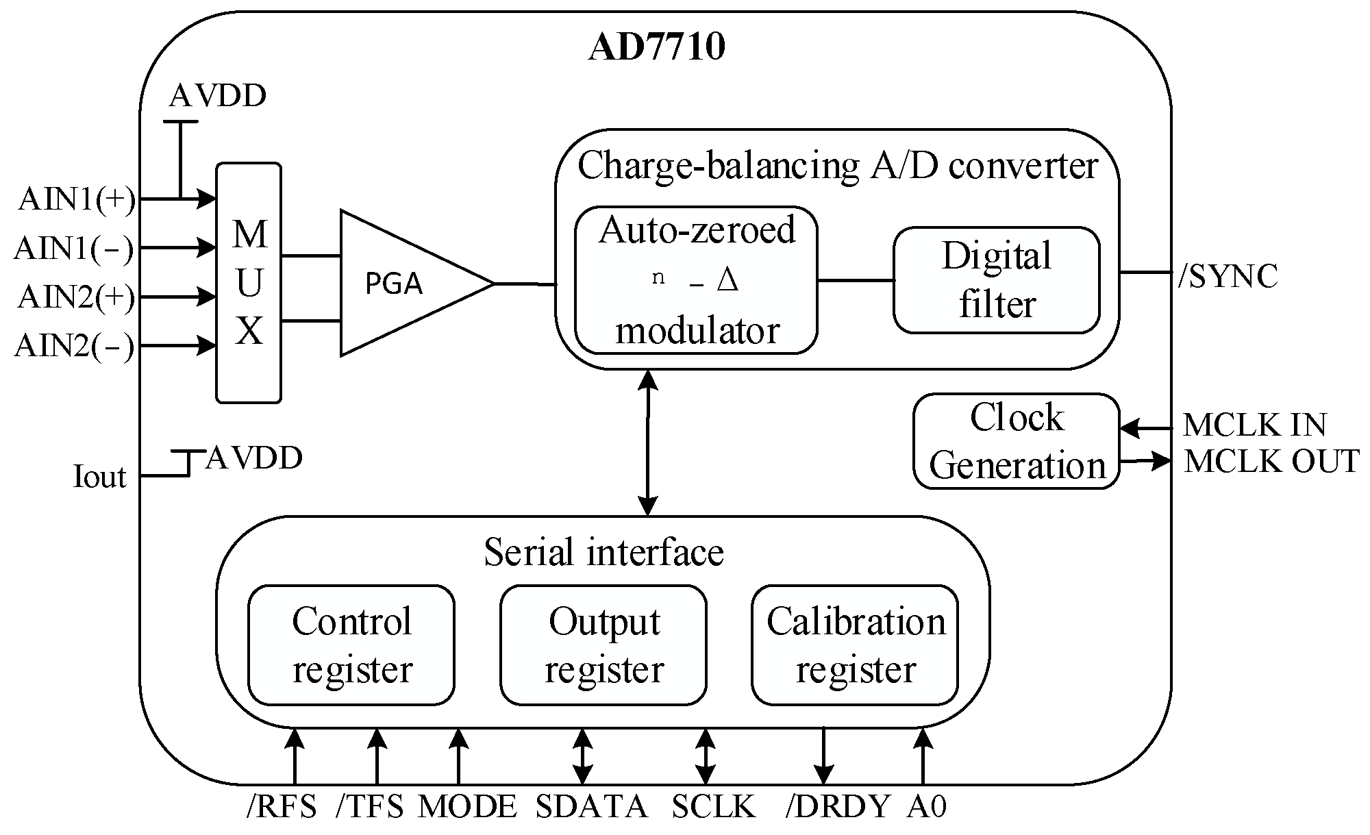
Figure 3.
The setup of a pulsed laser simulation of the SEFI experiment for the ADC.

Figure 4.
Register SEU cross-section. (a) The output register flip-flop cross-section; (b) the configuration register flip-flop cross-section.
Figure 4.
Register SEU cross-section. (a) The output register flip-flop cross-section; (b) the configuration register flip-flop cross-section.

Figure 5.
The impact of a bit flip in bits 0 to 11 of the configuration register on the ADC output. (a) The third bit of the configuration register flips; (b) the impact of a bit flip in bits 0 to 11 of the configuration register on the offset of the ADC output.
Figure 5.
The impact of a bit flip in bits 0 to 11 of the configuration register on the ADC output. (a) The third bit of the configuration register flips; (b) the impact of a bit flip in bits 0 to 11 of the configuration register on the offset of the ADC output.

Figure 6.
The impact of a bit flip in bits 12 to 17 of the configuration register on the ADC output. (a) The 12th bit of the configuration register flips; (b) the 16th bit of the configuration register flips.
Figure 6.
The impact of a bit flip in bits 12 to 17 of the configuration register on the ADC output. (a) The 12th bit of the configuration register flips; (b) the 16th bit of the configuration register flips.

Figure 7.
The impact of a bit flip in bits 18 to 23 of the configuration register on the ADC output. (a) The 19th bit of the configuration register flips; (b) the 22nd bit of the configuration register flips.
Figure 7.
The impact of a bit flip in bits 18 to 23 of the configuration register on the ADC output. (a) The 19th bit of the configuration register flips; (b) the 22nd bit of the configuration register flips.

Figure 8.
The impact of a bit flip in the calibration registers on the ADC output.
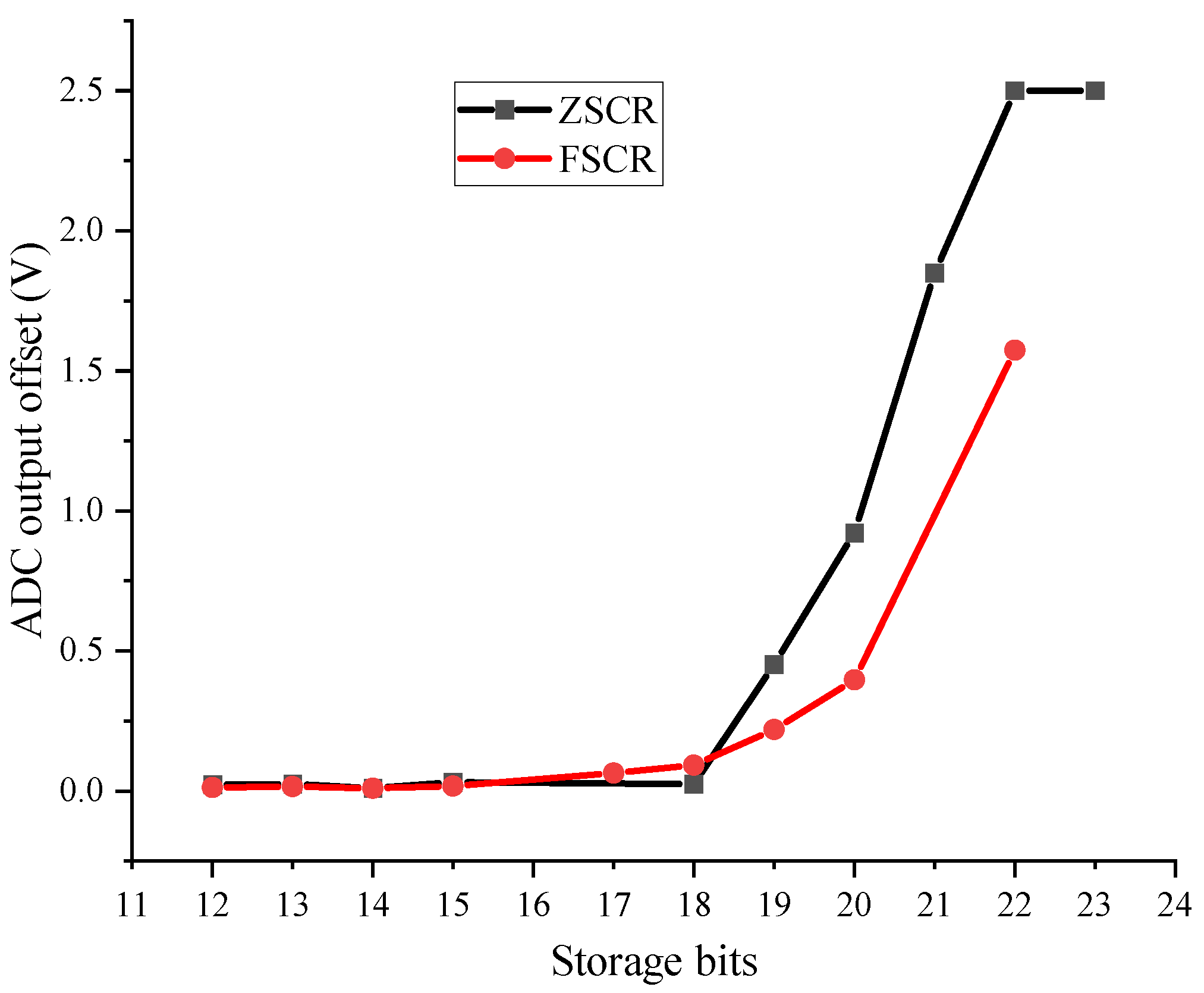
Figure 9.
The abnormal mainboard current caused by abnormal ADC pin current. (a) The case where A0, SLK, or TFS pins are configured as high impedance after the reconfiguration; (b) the case where the RFS pin has been configured as high impedance.
Figure 9.
The abnormal mainboard current caused by abnormal ADC pin current. (a) The case where A0, SLK, or TFS pins are configured as high impedance after the reconfiguration; (b) the case where the RFS pin has been configured as high impedance.

Figure 10.
The distribution of abnormal current points in AD7710.

Figure 11.
Schematic diagram of the parasitic PNPN latch-up structure in the RFS circuit.


Table 1.
The technical specifications of PPLSEE-1.
| Laser Wavelength | Typical Pulse Width | Beam Spot Size | Maximum Energy | Scanning Step Size | Repetition Rate | Energy Error Range |
|---|---|---|---|---|---|---|
| 1064 nm | 20 ps | 3 μm | 3 mJ | 5 μm | 1–10 kHz | <1% (8 h) |
Table 2.
Configuration register and calibration register write data and function.
| Number | Data (24 Bits) | Function |
|---|---|---|
| 1 | 22909C | Used to initialize the configuration register, ADC power-on self-calibration, unipolar input, the gain of 1, sampling channel of 2, first notch frequency of 100.16 Hz, the cut-off frequency of 26.2 Hz |
| 2 | C2909C | Enter the ZSCR read and write mode |
| 3 | E2909C | Enter FSCR read and write mode |
| 4 | 39E000 | ZSCR initialization data |
| 5 | 5E7000 | FSCR initialization data |
Table 3.
The function of each bit of the configuration register and the impact after flipping.
| Configuration Bits (24 bits) | Function | Flip Effect |
|---|---|---|
| 0~11 | Set the ADC filter cut-off frequency, the position of the first notch of the filter, and the data rate of the device. | Filter cut-off frequency and slew rate change |
| 12 | Input polarity setting, 0: Bipolar, 1: Unipolar | Input signal polarity changes |
| 13 | Burn-Out Current, 0: Off, 1: On | Unobservable |
| 14 | Output Compensation Current, 0: Off, 1: On | Unobservable |
| 15 | Output data word length setting, 0: 16-Bits, 1: 24-Bits | Not observed |
| 16 | Power-Down mode, 0: Normal Operation, 1: Power-Down | No data output |
| 17 | Sampling channel setting, 0: AIN1, 1: AIN2 | The sampling channel changes |
| 18–20 | Gain setting, (1, 2, 4, 8, 16, 32, 64, or 128) | Signal gain changes |
| 21–23 | Mode setting, can be set to normal, self-calibration, system calibration, background calibration, and other working modes | Work mode changes |
Disclaimer/Publisher’s Note: The statements, opinions and data contained in all publications are solely those of the individual author(s) and contributor(s) and not of MDPI and/or the editor(s). MDPI and/or the editor(s) disclaim responsibility for any injury to people or property resulting from any ideas, methods, instructions or products referred to in the content. |
© 2023 by the authors. Licensee MDPI, Basel, Switzerland. This article is an open access article distributed under the terms and conditions of the Creative Commons Attribution (CC BY) license (https://creativecommons.org/licenses/by/4.0/).
Share and Cite
MDPI and ACS Style
Mai, Z.; Zhu, X.; Li, H.; Han, J.; He, T. Experiment Study of Single Event Functional Interrupt in Analog-to-Digital Converters Using a Pulsed Laser. Electronics 2023, 12, 2774. https://doi.org/10.3390/electronics12132774
AMA Style
Mai Z, Zhu X, Li H, Han J, He T. Experiment Study of Single Event Functional Interrupt in Analog-to-Digital Converters Using a Pulsed Laser. Electronics. 2023; 12(13):2774. https://doi.org/10.3390/electronics12132774
Chicago/Turabian StyleMai, Ziqi, Xiang Zhu, Hongwei Li, Jianwei Han, and Tao He. 2023. "Experiment Study of Single Event Functional Interrupt in Analog-to-Digital Converters Using a Pulsed Laser" Electronics 12, no. 13: 2774. https://doi.org/10.3390/electronics12132774
Note that from the first issue of 2016, this journal uses article numbers instead of page numbers. See further details here.