
Improvement Breakdown Voltage by a Using Crown-Shaped Gate


1
School of Electrical Engineering, Pukyong National University, Busan 48513, Republic of Korea
2
School of Electrical Engineering, Hankyong National University, Anseong 17579, Republic of Korea
*
Authors to whom correspondence should be addressed.
†
These authors are contributed equally to this work.
Electronics 2023, 12(3), 474; https://doi.org/10.3390/electronics12030474
Submission received: 12 December 2022
/
Revised: 10 January 2023
/
Accepted: 13 January 2023
/
Published: 17 January 2023
(This article belongs to the Topic Advances in Microelectronics and Semiconductor Engineering)
Abstract
:In this paper, a crown-shaped trench gate formed by a sidewall spacer in insulated gate bipolar transistors (IGBT) is proposed to improve breakdown voltage. When a sidewall spacer is added to trench bottom corners, the electric field is distributed to the surface of the sidewall spacer and decreased to 48% peak value of the electric field. Thus, the sidewall spacer IGBT improved to 5% breakdown voltage. Another study proposed an additional oxide layer for trench bottom corners and improved breakdown voltage similar to the proposed IGBT. Previous studies have shown degradation in other electrical characteristics. However, this study shows a sidewall spacer IGBT that increases the current over 3% compared to a conventional trench IGBT when the applied gate voltage is under 4 V. Additionally, the turn-off loss characteristic is similar to conventional trench IGBT. Therefore, the breakdown voltage of the IGBT was improved while maintaining similar electrical properties to existing IGBTs through the crown-shaped gate.
1. Introduction
The advance of technology with respect to electrical systems heavily requires power semiconductors with the characteristic of high breakdown voltage [1]. Recently, power semiconductors that have a high breakdown voltage have been applied to electrical power transmission and distribution systems (HVDC) [2,3,4]. In addition, recent electric vehicles must operate to very high voltage conditions to charge [5,6,7]. Therefore, many researchers have attempted to improve the breakdown voltage of power semiconductors [8,9,10]. Normally, power semiconductors are separated to insulated gate bipolar transistors (IGBTs) and power metal-oxide-semiconductor field effect transistors (MOSFETs) [11,12,13]. In particular, IGBTs have very high breakdown voltages and improved turn-off characteristics compared to power MOSFETs. Therefore, IGBTs are widely used in power systems such as inverters, motor driver circuits and boost converters of uninterruptible power supplies (UPS), and the electric vehicle market places great importance on power semiconductors [14,15,16,17]. IGBTs with trench gates are especially used in a various fields because their collector-emitter saturation voltage (Von) is lower than that IGBTs with planar gates, because low Von causes a great trade-off in turn-off characteristics [18]. However, IGBTs with planar gates have a higher breakdown voltage than conventional trench gate IGBTs (C-IGBT) because the area of the trench gate causes a decreased electric field region [19]. Moreover, in IGBTs with trench gates, high electric field is concentrated on the bottom corners, causing a reduction in breakdown voltage [20]. Therefore, C–IGBTs have a drawback with respect to breakdown voltage degradation because of the electric field crowding (EFC), so other studies have proposed an increased radius of curvature in the trench corners to improve breakdown voltage [21]. Several studies have improved EFC without changing the radius of curvature in the trench gate, but these results cause increased fabrication process or degradation of C-IGBT characteristics [22].
In this study, we investigated a sidewall spacer with a trench gate IGBT (S-IGBT) for improved breakdown voltage [23]. S-IGBT has an expanded area of oxide region at the gate bottom, for decreased EFC effect on the bottom corners of the trench gate. Thus, the sidewall spacer reduces the peak value of the electric field and electrostatic potential on the bottom corners of trench gate. Therefore, we proposed a new IGBT by using a crown-shaped gate that improves breakdown voltage without changing the other electrical characteristics, and maintaining the characteristics of a C-IGBT.
2. Analysis of The Structure and Fabrication Method
2.1. Structure of the IGBT
The structures of a C-IGBT, S-IGBT and oxide IGBT (O-IGBT) are described in Figure 1. We have simulated the electrical characteristics of devices by using the Synopsys Sentaurus technology computer-aided design (TCAD) simulation tool, and we designed structures with the parameters in Table 1. The C-IGBT is a type of field-stop IGBT that uses various electrical systems. The S-IGBT simulation compares the thickness of the sidewall (TS) and the length of the sidewall (LS) as variable factors, and the sidewall spacer is located on the bottom corners of the trench gate. According to [24], an O-IGBT can improve breakdown voltage when optimizing the structure of a rectangular oxide layer without changing the other electrical characteristics. Therefore, we selected three variable factors—thickness of oxide layer (TO), length of oxide layer (LO), and depth from top of gate—for optimizing the rectangular oxide layer beneath the trench gate. The parameters of the S-IGBT and O-IGBT are very similar to the C-IGBT. The only difference between the C-IGBT, S-IGBT and O-IGBT is the existence of a sidewall spacer or oxide layer.
2.2. Applied Model in Simulation
Avalanche and Shockley–Read–Hall (SRH) generation-recombination models, Auger electron spectroscopy (AES) and avalanche generation (Lackner) were used as recombination models. Additionally, inversion and accumulation layer mobility (IALMob) and high-field saturation were used as mobility models to include the scattering effects of the channel mobility. To analyze the electrical and thermal characteristics, band-gap narrowing (BGN), thermodynamic and analytical expressions to calculate the thermoelectric power (AnalyticTEP) were used as physics [25,26].
2.3. Comparison Method
As mentioned earlier, the EFC effect reduces the breakdown voltage of an IGBT. To compare C-IGBTs, S-IGBTs and O-IGBTs thoroughly, the breakdown voltage of an O-IGBT was obtained by setting the widest variable range possible. We propose a method to improve the breakdown voltage characteristic of an O-IGBT, as previously described, using three variable factors. According to Figure 1d, O-IGBT showed between parameters of oxide layer and breakdown voltage, and we selected oxide parameters that showed the largest breakdown voltage. Thus, we compare other characteristics based on the TO of 0.5 µm and LO of 0.2 µm when the oxide layer depth from the gate is 2.85 µm. In addition, the value of the breakdown voltage decreases when the oxide layer is not at a depth from the gate at least 2.85 µm.
2.4. Fabrication Method
Figure 2 shows a possible fabrication process for the S-IGBT. First, the isolation step proceeds by using LOCOS for a secure semiconductor active region [27]. Second, photo resist (PR) is applied to the surface of the oxide layer and exposure light to the selected trench gate region [28,29]. Third, etching takes place at the region that was exposed to light during the second step. Fourth, oxide growth is started to form the gate dielectric. Fifth, to form the sidewall spacer, SiO2 is deposited on the top of the semiconductor. The crown-shaped gate uses the existing sidewall spacer process. SiO2 is deposited by using plasma-enhanced chemical vapor deposition (PECVD) [30]. Sixth, in order to eliminate the SiO2 film deposited with PECVD, SiO2 is selectively etched using CF4 with the same method as in the primary etching. The removal of the insulating film proceeds with ‘etch back’, which is a form of etching SiO2 covering the entire wafer surface without going through a photo process; thus, the sidewall spacer is formed [31,32,33,34]. Seventh, this fabrication uses poly-silicon because poly-silicon has variable advantages for gate material [35]. Therefore, poly-silicon is deposited to form the trench gate. In the last step, the residues of poly-silicon are etched, and the remaining fabrication steps proceed using the same process as the C-IGBT [36,37,38].
3. Results and Discussion
3.1. On-State Characteristics
Figure 3a shows the on-state Ic-Vg characteristic curves of a C-IGBT, S-IGBT and O-IGBT. When the collector voltage applied is 5 V, Ic-Vg curves are carried out. All simulations were performed at T = 300 K. In addition, we considered the surface roughness that appears in the trench gate. Therefore, when collector voltage and gate voltage were applied at 5 V, the channel electron mobility shows a result of 350 cm2 V−1 s−1 [39,40]. When gate voltage was applied under 4 V, the S-IGBT showed a higher current than the C-IGBT. However, when we applied gate voltage at 5 V, the collector current of the C-IGBT, S-IGBT and O-IGBT are 2570 A/cm2, 2240 A/cm2 and 946 A/cm2, respectively. Therefore, the S-IGBT showed little decrease in collector current with respect to C-IGBT; O-IGBT showed a much lower collector current than S-IGBT.
Figure 3b shows the collector current according to the sidewall spacer parameters when the collector voltage and gate voltage are applied at 5 V. High values of LS and TS decrease gate bias effect to the drift region. Therefore, the large size of the sidewall spacer interferes with channel formation. In the case of the S-IGBT, only a low LS is added on the bottom of the trench gate. Therefore, the S-IGBT is able to form a channel similar to the C-IGBT, so the Ic-Vg characteristic curves showed little difference between the S-IGBT and C-IGBT. However, the O-IGBT has a thicker oxide layer than the S-IGBT; it needs more gate voltage to achieve the same collector current. Therefore, large values of LS and TS caused a low collector current when we applied the same bias. When we applied a high gate voltage to each device, the difference between the C-IGBT, S-IGBT and O-IGBT accelerates more. Therefore, we used values of LS = 0.1 μm and TS = 0.7 μm to maintain electrical characteristics.
3.2. Breakdown Characteristics
Figure 4a shows that the electric field of the C-IGBT and S-IGBT are cut along the y-axis at a depth of 3.26 μm from the gate; we applied a gate voltage 15 V. The C-IGBT shows 217,836 V/cm, and 217,955 V/cm is the peak electric field on each bottom corner of the gate. However, the S-IGBT shows only 113,224 V/cm, and 113,409 V/cm is the peak electric field on each of the bottom corners of the gate. Therefore, the sidewall spacer reduces the peak electric field by almost 48%, and so improves the value of the breakdown voltage. Figure 4b shows the breakdown voltage characteristics of the C-IGBT, S-IGBT and O-IGBT. We can see that the breakdown voltage of the S-IGBT is 700 V, which is increased by 5% compared to that of the C-IGBT at 667 V. The O-IGBT showed a breakdown voltage of 704 V, which is increased by 5.5% compared to the C-IGBT. However, as previously described, the O-IGBT showed degradation of electrical characteristics. Therefore, the S-IGBT has more advantages with respect to electrical characteristics while having a similar breakdown voltage to the O-IGBT.
3.3. Trend in Breakdown Voltage
Figure 5a shows the breakdown voltage trend as the values of the sidewall spacer. The breakdown voltage shows an increase after decreasing from a specific point while the thickness of the sidewall spacer is increasing. We considered breakdown voltage by dividing it into three parts of increase in sidewall spacer thickness.
In case 1, when sidewall spacer thickness converges to zero the influence of the sidewall spacer is insignificant and similar to the C-IGBT. Therefore, the electric field is similar to the case in which only the trench gate exists, so the channel is formed by only one layer. However, as the TS increases and is smaller than the LS spacer, the electric field begins to be concentrated in only one region, as shown in Figure 5b. Therefore, electric field overlap is caused by increasing carrier density on the surface of the gate and low breakdown voltage.
In case 2, LS and TS are the in same condition, where the sidewall spacer exists in the quadrant form of a circle. Thus, electric field peak value is decreased because the electric field is not concentrated, as in case 1. However, the electric field is concentrated in two regions, as shown in Figure 5c. Therefore, some values of LS and TS showed almost the smallest breakdown voltage because they caused peak value of the electric field in the sidewall spacer. After sidewall spacer thickness is increased, electric field peak value decreases and the breakdown voltage is improved.
In case 3, if the value of LS is long enough, the electric field is distributed over a wider region. Therefore, breakdown voltage is increased instantly. Because the peak of the electric field region is separated by enough value of LS, the peak value of the electric field decreases. Some values of TS showed a slight decrease in the breakdown voltage and then an increase. Therefore, we apply a small value of LS to maintain on-state characteristics and enough value of TS for the electric field to be distributed over a wider region.
3.4. Turn-Off Characteristics
Figure 6a shows an example of a characteristic curve of the C-IGBT to calculate turn-off loss (Eoff). Collector voltage (Vce) and collector current (Ic) are as in Figure 6a. Eoff is defined as the integral of the product of current from the time corresponding to 10% of the current to the time corresponding to 10% of the voltage. Thus, Figure 6b shows power dissipation (Vce × Ic) and the filled area is the turn-off loss [41,42,43,44]. Figure 6c shows the comparison of the correlation trends between Eoff and on-state voltage drops of the C-IGBT, S-IGBT and O-IGBT. In IGBT, trend exists between Eoff and Von. This trend is generally used to evaluation method for IGBT. The trend curves can be acquired by changing the doping concentration of P-collector. Eoff tends to decrease as Von increases and the improvement structure to when the curve is closer to the origin. As a result, the Eoff of the S-IGBT is similar to that of the C-IGBT. Compared to the S-IGBT, the O-IGBT obtains a 23.7% decreased Von in the same operating conditions. As a result, this trade-off relationship can be described by gate controllability. That is, the gate controllability of the S-IGBT is weakened due to the sidewall spacer, compared to the C-IGBT. For this reason, the turn-off characteristic deteriorates. However, our proposed study only requires low values of TS and LS. Because the proposed IGBT uses lower values of TS and LS, our proposed S-IGBT shows a low increase in Eoff. Contrary to gate controllability, the breakdown voltage tends to be largely alleviated due to the sidewall spacer. Thus, breakdown voltage and Eoff have a trade-off relationship with each other, and the S-IGBT is likely to be an important key structure to adjust these characteristics.
4. Conclusions
To improve breakdown voltage, this paper presents a method that uses a crown-shaped gate using a sidewall spacer. The S-IGBT improves breakdown voltage while maintaining the Ion and Eoff of a C-IGBT. Based on the results, an S-IGBT reduces 48% of the peak value of the electric field on the bottom corners of the trench gate. As a result, a 5% increase in breakdown voltage occurs. Thus, by optimizing values of LS and TS, this study is able to increase the breakdown voltage without changing other electrical components. However, we considered LS and TS because the sidewall spacer effects electrical characteristics. Comparing with other studies with respect to improvement breakdown voltage, the S-IGBT maintained the electrical characteristics of a C-IGBT and had an easy fabrication process. Therefore, the crown-shaped gate has the potential to be the important key structure for the next generation, with high breakdown voltage and similar turn-off loss.
Author Contributions
Writing—original draft preparation, D.G.P.; supervision, H.K.; supervision, J.H.K. All authors have read and agreed to the published version of the manuscript.
Funding
This work was supported by a Research Grant of Pukyong National University (2022).
Data Availability Statement
This study reported a poster presented at NanoKorea Symposium 2022 and it was cited at reference [23].
Conflicts of Interest
The authors declare no conflict of interest.
References
- Sheng, K.; Williams, B.W.; Finney, S.J. A Review of IGBT Models. IEEE Trans. Power Electron. 2000, 15, 1250–1266. [Google Scholar] [CrossRef]
- Callavik, M.; Blomberg, A.; Häfner, J.; Jacobson, B. The Hybrid HVDC Breaker. ABB Grid Syst. Tech. Pap. 2012, 361, 143–152. [Google Scholar]
- Wang, H.; Ma, K.-W. IGBT Technology for Future High-Power VSC-HVDC Applications. In Proceedings of the 12th IET International Conference on AC and DC Power Transmission (ACDC 2016), Beijing, China, 28–29 May 2016. [Google Scholar]
- Trainer, D.R.; Davidson, C.C.; Oates, C.D.M.; Macleod, N.M.; Critchley, D.R.; Crookes, R.W. A New Hybrid Voltage-Sourced Converter for HVDC Power Transmission. In Proceedings of the CIGRÉ Session; CIGRE: Paris, France, 2010. [Google Scholar]
- Krein, P.T.; Roethemeyer, T.G.; White, R.A.; Masterson, B.R. Packaging and Performance of an IGBT-Based Hybrid Electric Vehicle. In Proceedings of the 1994 IEEE Workshop on Power Electronics in Transportation, Dearborn, MI, USA, 20–21 October 1994; pp. 47–52. [Google Scholar]
- Rosu, S.G.; Khalilian, M.; Cirimele, V.; Guglielmi, P. A Dynamic Wireless Charging System for Electric Vehicles Based on DC/AC Converters with SiC MOSFET-IGBT Switches and Resonant Gate-Drive. In Proceedings of the IECON 2016—42nd Annual Conference of the IEEE Industrial Electronics Society, Florence, Italy, 23–26 October 2016; pp. 4465–4470. [Google Scholar]
- Dimitrov, B.; Hayatleh, K.; Barker, S.; Collier, G.; Sharkh, S.; Cruden, A. A Buck-Boost Transformerless Dc–Dc Converter Based on IGBT Modules for Fast Charge of Electric Vehicles. Electronics 2020, 9, 397. [Google Scholar] [CrossRef] [Green Version]
- Ogura, T. Recent Technical Trends and Future Prospects of IGBTs and Power MOSFETs. In Proceedings of the 2014 International Power Electronics Conference (IPEC-Hiroshima 2014 ECCE-ASIA), Hiroshima, Japan, 18–21 May 2014; pp. 2068–2073. [Google Scholar]
- Rahimo, M. Future Trends in High-power Bipolar Metal-oxide Semi-conductor Controlled Power Semi-conductors. IET Circuits Devices Syst. 2014, 8, 155–167. [Google Scholar] [CrossRef]
- Liu, G.; Li, K.; Wang, Y.; Luo, H.; Luo, H. Recent Advances and Trend of HEV/EV-oriented Power Semiconductors—An Overview. IET Power Electron. 2020, 13, 394–404. [Google Scholar] [CrossRef]
- Baliga, B.J. Trends in Power Semiconductor Devices. IEEE Trans. Electron. Devices 1996, 43, 1717–1731. [Google Scholar] [CrossRef]
- Mueller, C.W.; Hilibrand, J. The “Thyristor”—A New High-Speed Switching Transistor. IRE Trans. Electron Devices 1958, 5, 2–5. [Google Scholar] [CrossRef]
- Liang, Y.C.; Samudra, G.S.; Huang, C.F. Insulated-Gate Bipolar Transistor. Power Microelectron. 2017, 191–248. [Google Scholar] [CrossRef]
- Aghdam, M.G.H.; Thiringer, T. Comparison of SiC and Si Power Semiconductor Devices to Be Used in 2.5 KW DC/DC Converter. In Proceedings of the 2009 International Conference on Power Electronics and Drive Systems (PEDS), Taipei, Taiwan, 2–5 November 2009; pp. 1035–1040. [Google Scholar]
- Shimizu, H.; Harada, J.; Bland, C. The Role of Optimized Vehicle Design and Power Semiconductor Devices to Improve the Performance of an Electric Vehicle. In Proceedings of the International Symposium on Power Semiconductor Devices and IC’s: ISPSD’95, Yokohama, Japan, 23–25 May 1995; pp. 8–12. [Google Scholar]
- Raj, J.S.S.S.; Sivaraman, P.; Prem, P.; Matheswaran, A. Wide Band Gap Semiconductor Material for Electric Vehicle Charger. Mater. Today Proc. 2021, 45, 852–856. [Google Scholar]
- Skibinski, G.; Evon, S.; Kempke, D.; Saunders, L. IGBT Drive Technology Demands New Motor and Cable Considerations. In Proceedings of the IEEE IAS Petroleum and Chemical Industry Conference, Philadelphia, PA, USA, 23–25 September 1996. [Google Scholar]
- Harada, M.; Minato, T.; Takahashi, H.; Nishihara, H.; Inoue, K.; Takata, I. 600 V Trench IGBT in Comparison with Planar IGBT-an Evaluation of the Limit of IGBT Performance. In Proceedings of the 6th International Symposium on Power Semiconductor Devices and ICs, Davos, Switzerland, 31 May–2 June 1994; pp. 411–416. [Google Scholar]
- Zhang, L.; Zhu, J.; Zhao, M.; Liu, S.; Sun, W.; Shi, L. Low-Loss SOI-LIGBT with Triple Deep-Oxide Trenches. IEEE Trans. Electron. Devices 2017, 64, 3756–3761. [Google Scholar] [CrossRef]
- Lee, J.-S.; Kang, E.-G.; Sung, M.-Y. Improvement of Electrical Characteristics of Vertical NPT Trench Gate IGBT Using Trench Emitter Electrode. J. Korean Inst. Electr. Electron. Mater. Eng. 2006, 19, 912–917. [Google Scholar] [CrossRef]
- Song, Q.; Yang, S.; Tang, G.; Han, C.; Zhang, Y.; Tang, X.; Zhang, Y.; Zhang, Y. 4H-SiC Trench MOSFET with L-Shaped Gate. IEEE Electron. Device Lett. 2016, 37, 463–466. [Google Scholar] [CrossRef]
- Lee, J.-S.; Kang, E.-G.; Sung, M.Y. Shielding Region Effects on a Trench Gate IGBT. Microelectron. J. 2008, 39, 57–62. [Google Scholar] [CrossRef]
- Park, D.-G.; Kim, J.-H. Improvement Breakdown Voltage by using Crown Shape Gate in IGBT. In Proceedings of the NanoKorea Symposium, Seoul, Republic of Korea, 6–8 July 2022; p. 578. [Google Scholar]
- Lee, J.I.; Choi, J.; Bae, Y.; Sung, M.Y. A Novel Trench IGBT with a Rectangular Oxide beneath the Trench Gate. In Proceedings of the 2009 1st Asia Symposium on Quality Electronic Design, Kuala Lumpur, Malaysia, 15–16 July 2009; pp. 370–373. [Google Scholar]
- Wu, Y.-C.; Jhan, Y.-R. Introduction of Synopsys Sentaurus TCAD Simulation. In 3D TCAD Simulation for CMOS Nanoeletronic Devices; Wu, Y.-C., Jhan, Y.-R., Eds.; Springer: Singapore, 2018; pp. 1–17. ISBN 978-981-10-3066-6. [Google Scholar]
- Watanabe, M.; Shigyo, N.; Hoshii, T.; Furukawa, K.; Kakushima, K.; Satoh, K.; Matsudai, T.; Saraya, T.; Takakura, T.; Itou, K. Impact of Three-Dimensional Current Flow on Accurate TCAD Simulation for Trench-Gate IGBTs. In Proceedings of the 2019 31st International Symposium on Power Semiconductor Devices and ICs (ISPSD), Shanghai, China, 19–23 May 2019; pp. 311–314. [Google Scholar]
- Lutze, J.W.; Perera, A.H.; Krusius, J.P. Field Oxide Thinning in Poly Buffer LOCOS Isolation with Active Area Spacings to 0.1 Μm. J. Electrochem. Soc. 1990, 137, 1867. [Google Scholar] [CrossRef]
- Abdolvand, R.; Ayazi, F. An Advanced Reactive Ion Etching Process for Very High Aspect-Ratio Sub-Micron Wide Trenches in Silicon. Sens. Actuators A Phys. 2008, 144, 109–116. [Google Scholar] [CrossRef]
- Abe, H.; Yoneda, M.; Fujiwara, N. Developments of Plasma Etching Technology for Fabricating Semiconductor Devices. Jpn. J. Appl. Phys. 2008, 47, 1435. [Google Scholar] [CrossRef]
- Kao, D.-B.; Mcvittie, J.P.; Nix, W.D.; Saraswat, K.C. Two-Dimensional Thermal Oxidation of Silicon: II. Modeling Stress Effects in Wet Oxides. IEEE Trans. Electron Devices 1988, 35, 25–37. [Google Scholar] [CrossRef]
- Dhong, S.H.; Petrillo, E.J. Sidewall Spacer Technology for MOS and Bipolar Devices. J. Electrochem. Soc. 1986, 133, 389. [Google Scholar] [CrossRef]
- Rodder, M.; Yeakley, D. Raised Source/Drain MOSFET with Dual Sidewall Spacers. IEEE Electron Device Lett. 1991, 12, 89–91. [Google Scholar] [CrossRef]
- Nam, K.S.; Lee, J.W.; Kim, S.-G.; Roh, T.M.; Park, H.S.; Koo, J.G.; Cho, K.I. A Novel Simplified Process for Fabricating a Very High Density P-Channel Trench Gate Power MOSFET. IEEE Electron Device Lett. 2000, 21, 365–367. [Google Scholar]
- Tsang, P.J.; Ogura, S.; Walker, W.W.; Shepard, J.F.; Critchlow, D.L. Fabrication of High-Performance LDDFET’s with Oxide Sidewall-Spacer Technology. IEEE J. Solid-State Circuits 1982, 17, 220–226. [Google Scholar] [CrossRef]
- Depp, S.W.; Juliana, A.; Huth, B.G. Polysilicon FET Devices for Large Area Input/Output Applications. In Proceedings of the 1980 International Electron Devices Meeting, Washington, DC, USA, 8–10 December 1980; pp. 703–706. [Google Scholar]
- Chang, H.R.; Baliga, B.J.; Kretchmer, J.W.; Piacente, P.A. Insulated Gate Bipolar Transistor (IGBT) with a Trench Gate Structure. In Proceedings of the 1987 International Electron Devices Meeting, Washington, DC, USA, 6–9 December 1987; pp. 674–677. [Google Scholar]
- Chang, H.-R.; Baliga, B.J. 500-V n-Channel Insulated-Gate Bipolar Transistor with a Trench Gate Structure. IEEE Trans. Electron Devices 1989, 36, 1824–1829. [Google Scholar] [CrossRef]
- Bartolf, H.; Mihaila, A.; Nistor, I.; Jurisch, M.; Leibold, B.; Zimmermann, M. Development of a 60 µm Deep Trench and Refill Process for Manufacturing Si-Based High-Voltage Super-Junction Structures. IEEE Trans. Semicond. Manuf. 2013, 26, 529–541. [Google Scholar] [CrossRef]
- Udrea, F.; Amaratunga, G.A.J. An On-State Analytical Model for the Trench Insulated Gate Bipolar Transistor (TIGBT). Solid State Electron. 1997, 41, 1111–1118. [Google Scholar] [CrossRef]
- Udrea, F.; Chan, S.S.M.; Thomson, J.; Keller, S.; Amaratunga, G.A.J.; Millington, A.D.; Waind, P.R.; Crees, D.E. Development of the next Generation of Insulated Gate Bipolar Transistors Based on Trench Technology. In Proceedings of the ESSDERC’97: 27th European Solid-State Device Research Conference, Stuttgart, Germany, 22–24 September 1997; pp. 504–507. [Google Scholar]
- Bauer, F.D. The Super Junction Bipolar Transistor: A New Silicon Power Device Concept for Ultra Low Loss Switching Applications at Medium to High Voltages. Solid-State Electron. 2004, 48, 705–714. [Google Scholar] [CrossRef]
- Kim, K.Y.; Noh, J.S.; Yoon, T.Y.; Kim, J.H. Improvement in Turn-Off Loss of the Super Junction IGBT with Separated n-Buffer Layers. Micromachines 2021, 12, 1422. [Google Scholar] [CrossRef]
- Chen, W.; Cheng, J. Study on the IGBT Using a Deep Trench Filled with SiO2 and High-k Dielectric Film. IEEE J. Electron Devices Soc. 2020, 8, 1025–1030. [Google Scholar] [CrossRef]
- Xu, X.; Chen, W.; Zhang, S.; Liu, C.; Sun, R.; Li, Z.; Zhang, B. Numerical Analysis for a P-Drift Region N-IGBT With Enhanced Dynamic Electric Field Modulation Effect. IEEE Trans. Electron. Devices 2022, 69, 3277–3282. [Google Scholar] [CrossRef]
Figure 1.
The structures of (a) C-IGBT, (b) S-IGBT and (c) O-IGBT. (d) breakdown voltage according to the oxide layer parameters in O-IGBT.
Figure 1.
The structures of (a) C-IGBT, (b) S-IGBT and (c) O-IGBT. (d) breakdown voltage according to the oxide layer parameters in O-IGBT.
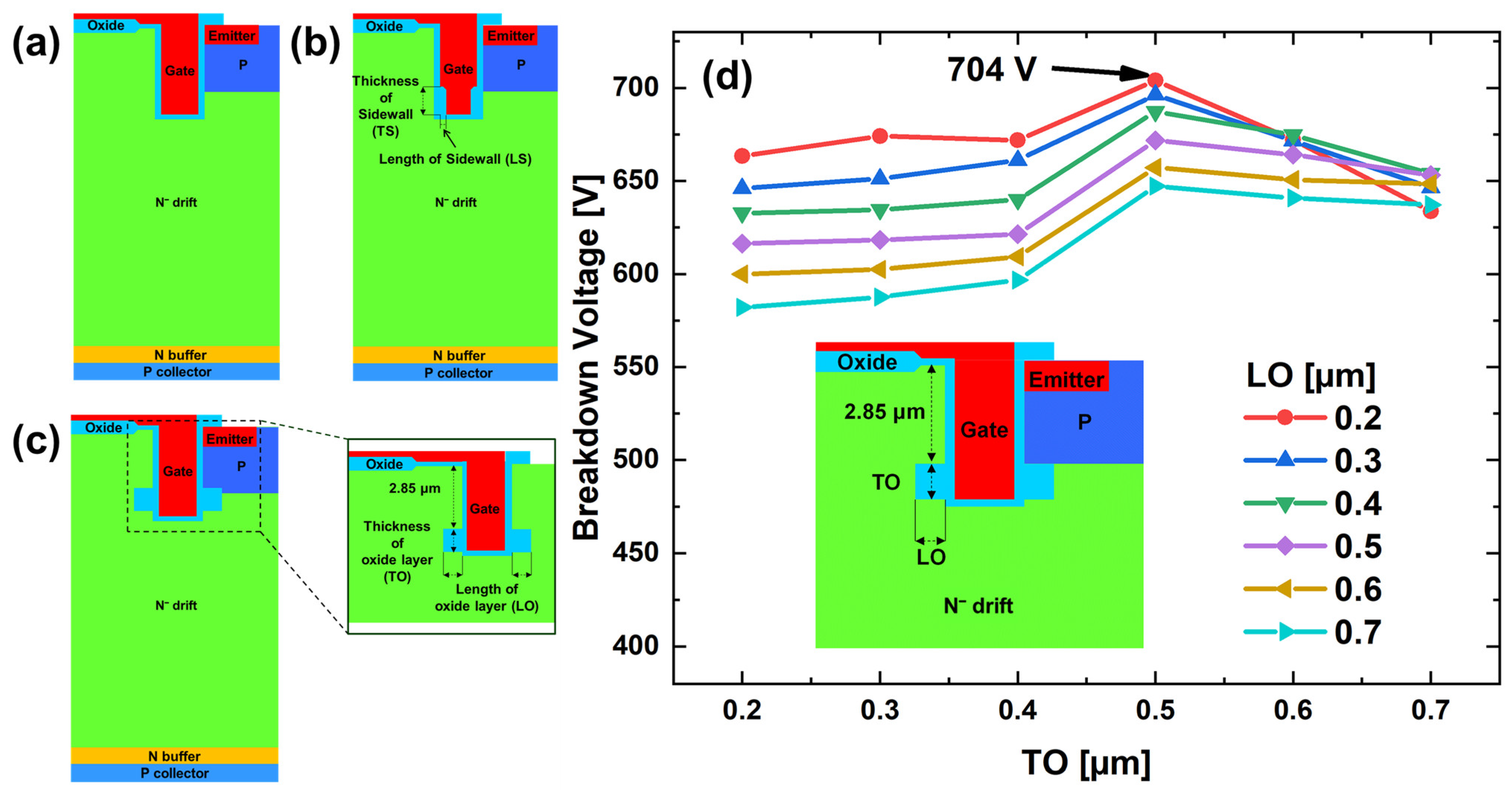
Figure 2.
A fabrication process of the S-IGBT. The crown-shaped gate can be fabricated without additional photo-lithography.
Figure 2.
A fabrication process of the S-IGBT. The crown-shaped gate can be fabricated without additional photo-lithography.

Figure 3.
(a) Ic-Vg characteristic curves of the C-IGBT, S-IGBT and O-IGBT. (b) Collector current according to the sidewall spacer parameters.
Figure 3.
(a) Ic-Vg characteristic curves of the C-IGBT, S-IGBT and O-IGBT. (b) Collector current according to the sidewall spacer parameters.

Figure 4.
(a) Electric field curves distributions of the C-IGBT and S-IGBT on the oxide surface. (b) Breakdown voltage characteristic curves of the C-IGBT and S-IGBT.
Figure 4.
(a) Electric field curves distributions of the C-IGBT and S-IGBT on the oxide surface. (b) Breakdown voltage characteristic curves of the C-IGBT and S-IGBT.

Figure 5.
(a) Breakdown voltage according to the sidewall spacer parameters. Electric field distribution when (b) TS = 0.1 µm and (c) TS = 0.2 µm, when each LS = 0.2 µm.
Figure 5.
(a) Breakdown voltage according to the sidewall spacer parameters. Electric field distribution when (b) TS = 0.1 µm and (c) TS = 0.2 µm, when each LS = 0.2 µm.

Figure 6.
The method to calculate the turn-off loss: (a) turn-off waveform of collector voltage, collector current and (b) power dissipation. (c) Turn-off loss curves between the C-IGBT, S-IGBT and O-IGBT at T = 300 K.
Figure 6.
The method to calculate the turn-off loss: (a) turn-off waveform of collector voltage, collector current and (b) power dissipation. (c) Turn-off loss curves between the C-IGBT, S-IGBT and O-IGBT at T = 300 K.


Table 1.
Device parameters for simulations.
| Parameter | C-IGBT | S-IGBT | O-IGBT |
|---|---|---|---|
| Width/Length | 4.8 µm | 4.8 µm | 4.8 µm |
| Length | 70.0 µm | 70.0 µm | 70.0 µm |
| Gate depth | 3.24 µm | 3.24 µm | 3.24 µm |
| Gate width | 0.8 µm | 0.8 µm | 0.8 µm |
| Depth of P-base | 2.5 µm | 2.5 µm | 2.5 µm |
| Depth of N+ emitter | 0.25 µm | 0.25 µm | 0.25 µm |
| Thickness of oxide | 0.02 µm | 0.02 µm | 0.02 µm |
| N buffer length | 2.5 µm | 2.5 µm | 2.5 µm |
| P-collector length | 0.5 µm | 0.5 µm | 0.5 µm |
| Length of sidewall | - | 0.1 µm | - |
| Thickness of sidewall | - | 0.7 µm | - |
| Depth of oxide layer | - | - | 2.85 µm |
| Oxide layer length | - | - | 0.2 µm |
| Oxide layer thickness | - | - | 0.5 µm |
| N+ emitter doping | 1 × 1021 cm−3 | 1 × 1021 cm−3 | 1 × 1021 cm−3 |
| P-base doping | 1 × 1018 cm−3 | 1 × 1018 cm−3 | 1 × 1018 cm−3 |
| P-collector doping | 1 × 1018 cm−3 | 1 × 1018 cm−3 | 1 × 1018 cm−3 |
| N− drift region doping | 3 × 1014 cm−3 | 3 × 1014 cm−3 | 3 × 1014 cm−3 |
Disclaimer/Publisher’s Note: The statements, opinions and data contained in all publications are solely those of the individual author(s) and contributor(s) and not of MDPI and/or the editor(s). MDPI and/or the editor(s) disclaim responsibility for any injury to people or property resulting from any ideas, methods, instructions or products referred to in the content. |
© 2023 by the authors. Licensee MDPI, Basel, Switzerland. This article is an open access article distributed under the terms and conditions of the Creative Commons Attribution (CC BY) license (https://creativecommons.org/licenses/by/4.0/).
Share and Cite
MDPI and ACS Style
Park, D.G.; Kim, H.; Kim, J.H. Improvement Breakdown Voltage by a Using Crown-Shaped Gate. Electronics 2023, 12, 474. https://doi.org/10.3390/electronics12030474
AMA Style
Park DG, Kim H, Kim JH. Improvement Breakdown Voltage by a Using Crown-Shaped Gate. Electronics. 2023; 12(3):474. https://doi.org/10.3390/electronics12030474
Chicago/Turabian StylePark, Dong Gyu, Hyunwoo Kim, and Jang Hyun Kim. 2023. "Improvement Breakdown Voltage by a Using Crown-Shaped Gate" Electronics 12, no. 3: 474. https://doi.org/10.3390/electronics12030474
Note that from the first issue of 2016, this journal uses article numbers instead of page numbers. See further details here.