

An Electronically Reconfigurable Highly Selective Stop-Band Ultra-Wideband Antenna Applying Electromagnetic Bandgaps and Positive-Intrinsic-Negative Diodes

 ,
,  ,
,  ,
,  ,
,
Abstract
:1. Introduction
2. Antenna Design Procedure
2.1. Design of UWB Antenna with Quasi-Perfect Stop-Band Bands at 3.4–3.8 GHz and WLAN Band
2.2. P-I-N Diodes
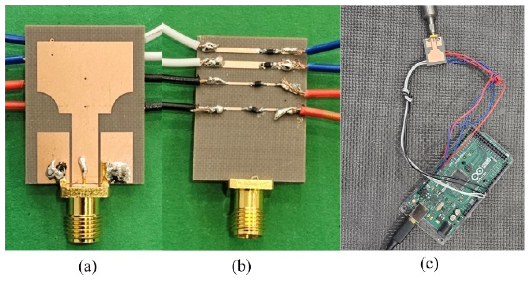
2.3. Design of Reconfigurable UWB Antenna
2.4. Reconfigurable Characteristics of Notched-Band Antenna
2.4.1. Case 1: UWB Antenna without Any Rejection Band
2.4.2. Case 2: Reconfiguration of UWB Antennas with WLAN Stop Bands
2.4.3. Case 3: Reconfiguration of UWB Antennas with 5G Sub-6 GHz Stop Band
2.4.4. Case 4: Reconfigurable Dual Quasi-Perfect Stop-Band UWB Antenna
2.4.5. Controllability of Stop-Band Bandwidth
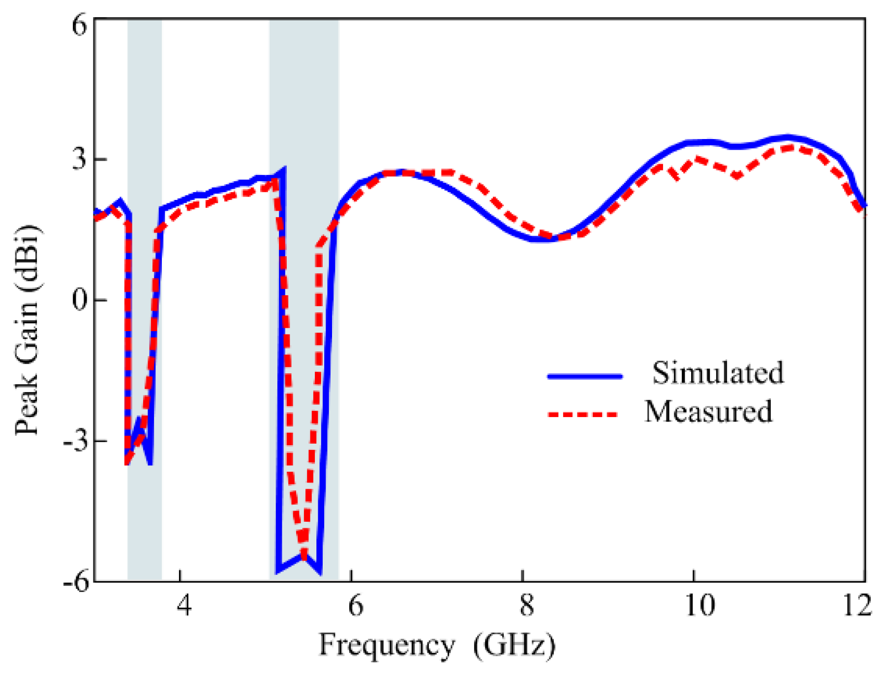
3. Results and Discussion
4. Conclusions
Author Contributions
Funding
Data Availability Statement
Conflicts of Interest
References
- Win, M.Z.; Dardari, D.; Molisch, A.F.; Wiesbeck, W.; Jinyun Zhang, W. History and Applications of UWB; Institute of Electrical and Electronics Engineers: Piscataway, NJ, USA, 2009. [Google Scholar]
- Win, M.Z. Spectral Density of Random Time-Hopping Spread-Spectrum UWB Signals with Uniform Timing Jitter. IEEE Commun. Lett. 1999, 2, 36–38. [Google Scholar] [CrossRef]
- Soerbakti, Y.; Syahputra, R.F.; Gamal, M.D.H.; Irawan, D.; Putra, E.H.; Darwis, R.S. Improvement of low-profile microstrip antenna performance by hexagonal-shaped SRR structure with DNG metamaterial characteristic as UWB application. Alex. Eng. J. 2022, 61, 4241–4252. [Google Scholar]
- Din, I.U.; Ullah, W.; Abbasi, N.A.; Ullah, S.; Shihzad, W.; Khan, B.; Jayakody, D.N.K. A Novel Compact Ultra-Wideband Frequency-Selective Surface-Based Antenna for Gain Enhancement Applications. J. Electromagn. Eng. Sci. 2023, 23, 108–121. [Google Scholar] [CrossRef]
- Srikanth, B.S.; Gurung, S.B.; Manu, S.; Gowthami, G.N.S.; Ali, T.; Pathan, S. A slotted UWB monopole antenna with truncated ground plane for breast cancer detection. Alex. Eng. J. 2020, 59, 3767–3780. [Google Scholar]
- Wang, L.; Li, Z.; Zheng, H. Investigation of Parallel and Orthogonal MIMO Antennas with Two-Notched Structures for Ultra-Wideband Application. Micromachines 2023, 14, 1406. [Google Scholar] [CrossRef] [PubMed]
- Abbas, A.; Hussain, N.; Jeong, M.J.; Park, J.; Shin, K.S.; Kim, T.; Kim, N. A Rectangular Notch-Band UWB Antenna with Controllable Notched Bandwidth and Centre Frequency. Sensors 2020, 20, 777. [Google Scholar] [CrossRef] [PubMed]
- Youn, S.; Jang, B.J.; Choo, H. Design of a UWB Antenna with Multiple Ports on a Single Circular Radiator for Direction-Finding Applications. J. Electromagn. Eng. Sci. 2023, 23, 63–68. [Google Scholar] [CrossRef]
- Vallappil, A.K.; Khawaja, B.A.; Rahim, M.K.A.; Iqbal, M.N.; Chattha, H.T.; Ali, M.F.B.M. A compact triple-band UWB inverted triangular antenna with dual-notch band characteristics using SSRR metamaterial structure for use in next-generation wireless systems. Fractal Fract. 2022, 6, 422. [Google Scholar] [CrossRef]
- Ding, Y.; Li, M.; Su, J.; Guo, Q.; Yin, H.; Li, Z.; Song, J. Ultrawideband Frequency-Selective Absorber Designed with An Adjustable and Highly Selective Notch. IEEE Trans. Antennas Propag. 2020, 69, 1493–1504. [Google Scholar] [CrossRef]
- Wang, C.H.; Shi, X.M. Miniaturized tri-notched wideband bandpass filter with ultrawide upper stopband suppression. Sci. Rep. 2021, 11, 13004. [Google Scholar] [CrossRef]
- Abbas, A.; Hussain, N.; Sufian, M.A.; Jung, J.; Park, S.M.; Kim, N. Isolation and Gain Improvement of a Rectangular Notch UWB-MIMO Antenna. Sensors 2022, 22, 1460. [Google Scholar] [CrossRef] [PubMed]
- Abbas, A.; Sufian, M.A.; Jung, J.; Uktam, A.; Lee, J.; Kim, N. A Triple Band Notched UWB MIMO Antenna with Improved Performance. In Proceedings of the 2022 Asia-Pacific Microwave Conference (APMC), Yokohama, Japan, 29 November–2 December 2022; pp. 482–484. [Google Scholar]
- Alazemi, A.J.; Alsaleh, Y.T. An ultrawideband antenna with two independently tunable notch bands. Alex. Eng. J. 2023, 79, 402–410. [Google Scholar] [CrossRef]
- Abbas, A.; Hussain, N.; Sufian, M.A.; Awan, W.A.; Jung, J.; Lee, S.M.; Kim, N. Highly Selective Multiple-Notched UWB-MIMO Antenna with Low Correlation Using an Innovative Parasitic Decoupling Structure. Eng. Sci. Technol. Int. J. 2023, 43, 101440. [Google Scholar] [CrossRef]
- Mabrouk, A.M.; Ibrahim, A.A.; Hamed, H.F. Reconfigurable antenna with frequency and beam switching using transformer oil and PIN-diode for microwave applications. Alex. Eng. J. 2022, 61, 1824–1833. [Google Scholar] [CrossRef]
- Awan, W.A.; Hussain, N.; Kim, S.; Kim, N. A Frequency-Reconfigurable Filtenna for GSM, 4G-LTE, ISM, and 5G Sub-6 GHz Band Applications. Sensors 2022, 22, 5558. [Google Scholar] [CrossRef] [PubMed]
- Abutarboush, H.F.; Nilavalan, R.; Cheung, S.W.; Nasr, K.M.; Peter, T.; Budimir, D.; Al-Raweshidy, H. A Reconfigurable Wideband and Multiband Antenna Using Dual-Patch Elements for Compact Wireless Devices. IEEE Trans. Antennas Propag. 2011, 60, 36–43. [Google Scholar] [CrossRef]
- Prabhu, P.; Subramani, M.; Kwak, K.S. Analysis of Integrated UWB MIMO And CR Antenna System Using Transmission Line Model with Functional Verification. Sci. Rep. 2022, 12, 14128. [Google Scholar] [CrossRef] [PubMed]
- Chao, Z.; Zitong, Z.; Pei, X.; Jie, Y.; Zhu, L.; Gaosheng, L. A Miniaturized Microstrip Antenna with Tunable Double Band-Notched Characteristics for UWB Applications. Sci. Rep. 2022, 12, 19703. [Google Scholar] [CrossRef] [PubMed]
- Hu, F.; Chen, B.; Zhu, K. Full Spectrum Sharing in Cognitive Radio Networks Toward 5G: A Survey. IEEE Access 2018, 6, 15754–15776. [Google Scholar] [CrossRef]
- Cabric, D.O.; Donnell, I.D.; Chen, M.W.; Brodersen, R.W. Spectrum Sharing Radios. IEEE Circuits Syst. Mag. 2006, 6, 30–45. [Google Scholar] [CrossRef]
- Boukarkar, A.; Rachdi, S.; Amine, M.M.; Sami, B.; Khalil, A.B. A Compact Four State Radiation-Pattern Reconfigurable Monopole Antenna for Sub-6 Ghz IoT Applications. AEU Int. J. Electron. Commun. 2023, 158, 154467. [Google Scholar] [CrossRef]
- Tang, X.L.; Zhang, Q.; Hu, S.; Ge, S.; Chen, Y.; Yu, H. Beam Steering Using Momentum Reconfigurable Goubau Meta-Line Radiators. Sci. Rep. 2018, 8, 11854. [Google Scholar] [CrossRef]
- Arshad, F.; Ahmad, A.; Amin, Y.; Abbasi, M.A.B.; Choi, D.Y. MIMO Antenna Array with The Capability of Dual Polarization Reconfiguration for 5G Mm-Wave Communication. Sci. Rep. 2022, 12, 18298. [Google Scholar] [CrossRef] [PubMed]
- Ushikoshi, D.; Higashiura, R.; Tachi, K.; Fathnan, A.A.; Mahmood, S.; Takeshita, H.; Homma, H.; Akram, M.R.; Vellucci, S.; Lee, J.; et al. Pulse-Driven Self-Reconfigurable Meta-Antennas. Nat. Commun. 2023, 14, 633. [Google Scholar] [CrossRef]
- Khan, M.S.; Iftikhar, A.; Shubair, R.M.; Capobianco, A.D.; Asif, S.M.; Braaten, B.D.; Anagnostou, D.E. Ultra-Compact Reconfigurable Band Reject UWB MIMO Antenna with Four Radiators. Electronics 2020, 9, 584. [Google Scholar] [CrossRef]
- Hussain, N.; Ghaffar, A.; Naqvi, S.I.; Iftikhar, A.; Anagnostou, D.E.; Tran, H.H. A Conformal Frequency Reconfigurable Antenna with Multiband and Wideband Characteristics. Sensors 2022, 22, 2601. [Google Scholar] [CrossRef]
- Modak, S.; Daasari, S.; Shome, P.P.; Khan, T. Switchable/Tunable Band-Notched Characteristics in UWB And UWB-MIMO Antennas: A Comprehensive Review. Wirel. Pers. Commun. 2023, 128, 2131–2154. [Google Scholar] [CrossRef]
- Bai, Y.; Gardner, P.; He, Y.; Sun, H. A Surrogate Modeling Approach for Frequency Reconfigurable Antennas. IEEE Trans. Antennas Propag. 2023, 71, 5498–5503. [Google Scholar] [CrossRef]
- Zaidi, A.; Ghaffar, A.; Alzaidi, M.S.; Alsharef, M.; Elkamchouchi, D.H.; Ghoneim, S.S.; Alharbi, T.E. A Low Profile Ultra-Wideband Antenna with Reconfigurable Notch Band Characteristics for Smart Electronic Systems. Micromachines 2022, 13, 1803. [Google Scholar] [CrossRef]
- Niture, D.V.; Mahajan, S.P. A Compact Reconfigurable Antenna for UWB and Cognitive Radio Applications. Wirel. Pers. Commun. 2022, 125, 3661–3679. [Google Scholar] [CrossRef]
- Anagnostou, D.E.; Chryssomallis, M.T.; Braaten, B.D.; Ebel, J.L.; Sepúlveda, N. Reconfigurable UWB Antenna With RF-MEMS For On-Demand WLAN Rejection. IEEE Trans. Antennas Propag. 2013, 62, 602–608. [Google Scholar] [CrossRef]
- Boudaghi, H.; Azarmanesh, M.; Mehranpour, M. A Frequency-Reconfigurable Monopole Antenna Using Switchable Slotted Ground Structure. IEEE Antennas Wirel. Propag. Lett. 2012, 11, 655–658. [Google Scholar] [CrossRef]
- Bahrami, S.; Moloudian, G.; Song, H.J.; Buckley, J.L. Reconfigurable UWB Circularly Polarized Slot Antenna with Three Modes of Operation and Continuous Tuning Rang. IEEE Trans. Antennas Propag. 2022, 70, 8542–8547. [Google Scholar] [CrossRef]
- Horestani, A.K.; Shaterian, Z.; Naqui, J.; Martin, F.; Fumeaux, C. Reconfigurable and Tunable S-Shaped Split-Ring Resonators and Application in Band-Notched UWB Antennas. IEEE Trans. Antennas Propag. 2016, 64, 3766–3776. [Google Scholar] [CrossRef]
- Kingsly, S.; Thangarasu, D.; Kanagasabai, M.; Alsath, M.G.N.; Palaniswamy, S.K.; Rao, T.R.; Subbaraj, S.; Selvam, Y.P.; Sambandam, P.; Ganesan, G. Tunable Band-Notched High Selective UWB Filtering Monopole Antenna. IEEE Trans. Antennas Propag. 2019, 67, 5658–5661. [Google Scholar] [CrossRef]
- Lakrit, S.; Das, S.; El Alami, A.; Barad, D.; Mohapatra, S. A Compact UWB Monopole Patch Antenna with Reconfigurable Band-Notched Characteristics for Wi-MAX And WLAN Applications. AEU Int. J. Electron. Commun. 2019, 105, 106–115. [Google Scholar] [CrossRef]
- Abbas, A.; Hussain, N.; Lee, J.; Park, S.G.; Kim, N. Triple Rectangular Notch UWB Antenna Using EBG and SRR. IEEE Access 2021, 9, 2508–2515. [Google Scholar] [CrossRef]
- Samineni, P.; Khan, T.; De, A. Modeling of electromagnetic band gap structures: A review. Int. J. RF Microw. Comput.-Aided Eng. 2017, 27, e21055. [Google Scholar] [CrossRef]
- Sharma, S.; Tripathi, C.C. Frequency reconfigurable U-slot antenna for SDR application. Prog. Electromagn. Res. Lett. 2015, 55, 129–136. [Google Scholar] [CrossRef]
- Dalal, K.; Singh, T.; Singh, P.K. A Low Profile Ultra-Wideband Antenna Design with Reconfigurable Notch-Bands for Wideband and Narrowband Applications. Wirel. Pers. Commun. 2022, 125, 1405–1423. [Google Scholar] [CrossRef]
- Sharma, K.; Karmakar, A.; Sharma, M.; Chauhan, A.; Bansal, S.; Hooda, M.; Kumar, S.; Gupta, N.; Singh, A.K. Reconfigurable Dual Notch Band Antenna on Si-Substrate Integrated with RF MEMS SP4T Switch For GPS, 3G, 4G, Bluetooth, UWB and Close-Range Radar Applications. AEU Int. J. Electron. Commun. 2019, 110, 152873. [Google Scholar] [CrossRef]
- Tewary, T.; Maity, S.; Mukherjee, S.; Roy, A.; Sarkar, P.P.; Bhunia, S. Design of High-Gain Broadband Microstrip Patch Antenna for UWB/X/Ku Band Applications. AEU Int. J. Electron. Commun. 2021, 139, 153905. [Google Scholar] [CrossRef]
- Sumana, L.; Sundarsingh, E.F.; Priyadharshini, S. Shape Memory Alloy-Based Frequency Reconfigurable Ultrawideband Antenna for Cognitive Radio Systems. IEEE Trans. Compon. Packag. Manuf. Technol. 2020, 11, 3–10. [Google Scholar] [CrossRef]
- Nan, J.; Zhao, J.; Gao, M.; Yang, W.; Wang, M.; Xie, H. A Compact 8-States Frequency Reconfigurable UWB Antenna. IEEE Access 2021, 9, 144257–144263. [Google Scholar] [CrossRef]
- Saha, C.; Shaik, L.A.; Muntha, R.; Antar, Y.M.; Siddiqui, J.Y. A Dual Reconfigurable Printed Antenna: Design Concept and Experimental Realization. IEEE Antennas Propag. Mag. 2018, 60, 66–74. [Google Scholar] [CrossRef]
- Jin, G.; Deng, C.; Xu, Y.; Yang, J.; Liao, S. Differential Frequency-Reconfigurable Antenna Based on Dipoles for Sub-6 Ghz 5G And WLAN Applications. IEEE Antennas Wirel. Propag. Lett. 2020, 19, 472–476. [Google Scholar] [CrossRef]
- Quddious, A.; Abbasi, M.A.B.; Antoniades, M.A.; Vryonides, P.; Fusco, V.; Nikolaou, S. Dynamically Reconfigurable UWB Antenna Using an FET Switch Powered by Wireless RF Harvested Energy. IEEE Trans. Antennas Propag. 2020, 68, 5872–5881. [Google Scholar] [CrossRef]


| States | D1 | D2 | D3 | D4 | Notch Bands | Characteristics |
|---|---|---|---|---|---|---|
| I | OFF | OFF | OFF | OFF | None | Entire UWB band |
| II | ON | ON | ON | ON | Dual notch band | Dual-notch-band UWB antenna |
| III | ON | ON | OFF | OFF | Single | Single-notch-band UWB antenna |
| IV | OFF | OFF | ON | ON | Single | Single-notch-band UWB antenna |
| States | D1 | D2 | D3 | D4 | Notch Bandwidth (GHz) | Characteristics |
|---|---|---|---|---|---|---|
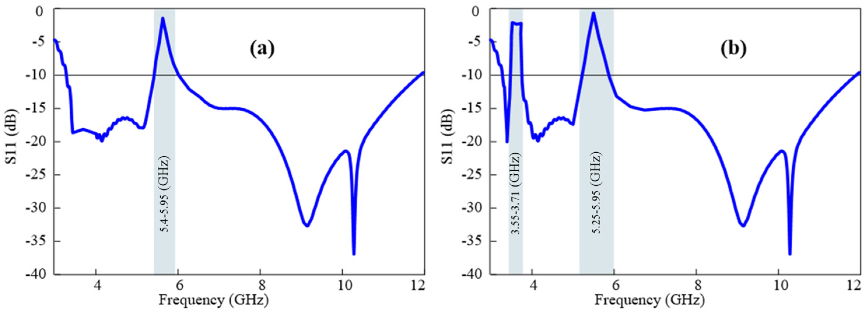
| I | OFF | OFF | OFF | ON | 5.4–5.95 | Conventional WLAN notched band |
| II | OFF | OFF | ON | OFF | 5–5.5 | Conventional WLAN notched band |
| III | OFF | ON | OFF | OFF | 3.55–3.71 | Conventional 5G notched band |
| IV | ON | OFF | OFF | OFF | 3.39–3.6 | Conventional 5G notched band |
| States | D1 | D2 | D3 | D4 | Notch Bandwidth (GHz) | Characteristics |
|---|---|---|---|---|---|---|
| I | ON | ON | ON | OFF | 3.4–3.8, 5–5.5 | Sharp 5G and regular WLAN notched |
| II | ON | ON | OFF | ON | 3.4–3.8, 5.4–5.95 | Sharp 5G and regular WLAN notched |
| III | ON | OFF | ON | ON | 3.55–3.71, 5.25–5.75 | Regular 5G and sharp WLAN notched |
| IV | ON | OFF | OFF | OFF | 3.39–3.6, 5.25–5.75 | Regular 5G and sharp WLAN notched |
| Ref. | Ant. Dimensions (mm2) | Bandwidth GHz | Notch Bandwidth GHz | Notch Selectivity | Notch Band Controllability | Notch Band Minimum Gain (dB) |
|---|---|---|---|---|---|---|
| [42] | 24 × 24 | 3.1–10.6 | 3.1–3.65 4.9–5.56 5.9–6.4 7.3–8.5 | low | no | −1 | −4 | −1 | 1 |
| [43] | 44.1 × 60 | 0.68–16.23 | 3.3–3.80 5.15–5.35 | low | no | −6 | −7 |
| [44] | 49.4 × 35 | 5–24.5 | N/A | low | no | Not provided |
| [45] | 58 × 60 | 3.4–10.2 | 4.7–5.1 5.3–6.0 | low | no | Not provided |
| [46] | 22 × 13 | 2.82–13.25 | 3.19–4.58 5.26–6.21 7.87–8.73 | low | no | −6 | −1 | −3 |
| [47] | 50 × 50 | 2.6–10.8 | 6.66, 8.34 9.85 | low | no | Not provided |
| [48] | 50 × 50 | 2.89–4.07 5.1–6.19 | N/A | N/A | N/A | Not provided |
| [49] | 27 × 33 | 5–6.1 | 5.6 | low | low | −1.5 |
| Prop. | 26 × 20 | 3–11.6 | 3.4–3.8 5.25–5.75 | high | yes | −3 | −5.8 |
Disclaimer/Publisher’s Note: The statements, opinions and data contained in all publications are solely those of the individual author(s) and contributor(s) and not of MDPI and/or the editor(s). MDPI and/or the editor(s) disclaim responsibility for any injury to people or property resulting from any ideas, methods, instructions or products referred to in the content. |
© 2024 by the authors. Licensee MDPI, Basel, Switzerland. This article is an open access article distributed under the terms and conditions of the Creative Commons Attribution (CC BY) license (https://creativecommons.org/licenses/by/4.0/).
Share and Cite
Abbas, A.; Hussain, N.; Sufian, M.A.; Awan, W.A.; Lee, J.; Kim, N. An Electronically Reconfigurable Highly Selective Stop-Band Ultra-Wideband Antenna Applying Electromagnetic Bandgaps and Positive-Intrinsic-Negative Diodes. Micromachines 2024, 15, 638. https://doi.org/10.3390/mi15050638
Abbas A, Hussain N, Sufian MA, Awan WA, Lee J, Kim N. An Electronically Reconfigurable Highly Selective Stop-Band Ultra-Wideband Antenna Applying Electromagnetic Bandgaps and Positive-Intrinsic-Negative Diodes. Micromachines. 2024; 15(5):638. https://doi.org/10.3390/mi15050638
Chicago/Turabian StyleAbbas, Anees, Niamat Hussain, Md. Abu Sufian, Wahaj Abbas Awan, Jaemin Lee, and Nam Kim. 2024. "An Electronically Reconfigurable Highly Selective Stop-Band Ultra-Wideband Antenna Applying Electromagnetic Bandgaps and Positive-Intrinsic-Negative Diodes" Micromachines 15, no. 5: 638. https://doi.org/10.3390/mi15050638