Article

Model Parameters and Degradation Mechanism Analysis of Indium Phosphide Hetero-Junction Bipolar Transistors Exposed to Proton Irradiation

1
School of Aviation Engineering, Air Force Engineering University, Xi’an 710051, China
2
School of Air Defense and Antimissile, Air Force Engineering University, Xi’an 710051, China
3
School of Nuclear Science and Technology, Xi’an Jiaotong University, Xi’an 710049, China
4
LONGi Green Energy Technology Co., Ltd., Xi’an 710018, China
*
Authors to whom correspondence should be addressed.
Electronics 2024, 13(10), 1831; https://doi.org/10.3390/electronics13101831
Submission received: 23 March 2024 / Revised: 26 April 2024 / Accepted: 5 May 2024 / Published: 9 May 2024

Abstract

:
The degradation properties of Indium phosphide hetero-junction bipolar transistors (InP HBTs) under proton irradiation are studied and modelled using a compact model for pre-irradiation, post-irradiation, and post-annealing. The variation rates of the model parameters, such as the base–emitter saturation current (ISE) and ideality factor in the ideal region (NE) in the forward Gummel characteristics, the zero-biased capacitance (Cje) and the grading factor (Mjer) in the BE junction capacitance, and the transit time parameter in the base region (Tfb), are analysed to delve into the degradation mechanism induced by proton irradiation. The displacement damage, induced by proton irradiation in the space charge region of the base–emitter junction and in the quasi-neutral bulk base region, is found to be responsible for the decrease in current gain and cut-off frequency. After annealing, the variation rates of the parameters decrease significantly compared to post-irradiation. This suggests that the recombination of unstable defects leads to a slight recovery in the degradation characteristics of InP HBTs after a period of annealing.

1. Introduction

Indium phosphide hetero-junction bipolar transistors (InP HBTs) are extensively used in aerospace systems, military communications and satellites owing to their exceptional material properties and high-frequency characteristics within various millimetre-wave devices [1,2,3]. However, in the harsh irradiation environment of space, InP HBTs are susceptible to single-event transients (SETs) triggered by heavy ions [4,5,6] and displacement damage induced by high-flux protons [7,8]. While our previous work has covered research on the single-event effect [9], this paper will concentrate on displacement damage.
Multiple energetic protons can induce displacement damage when striking microelectronic devices, particularly in aerospace systems operating within the inner Van Allen radiation belts over prolonged periods of time [10]. These displacement defects include host atoms displacement, lattice damage and the formation of deep-level traps [11,12]. The reported studies primarily delineated and analysed experimental phenomena [7,13,14], with limited literature delving into the irradiation-induced degradation mechanism through compact models. Lawal O M et al. discussed the Simulation Program with Integrated Circuit Emphasis (SPICE) model parameters of a pre- and post-irradiated silicon bipolar junction transistor (Si BJT) [15]. Petrosyants K et al. explored the SPICE model of a Si BJTs and silicon germanium (SiGe) hetero-junction bipolar transistor (HBTs), taking into account the total irradiation dose effects with gamma-ray, proton, neutron, and electron irradiation [16,17,18]. Van Uffelen M et al. studied the direct current (DC) characteristics of SiGe HBTs at gamma doses of up to 4 MGy using the SPICE model [19]. Zhang J C et al. investigated the impact of gamma irradiation on the DC and alternating current (AC) characteristics of gallium arsenide (GaAs) and InP hetero-junction bipolar transistors with the VBIC and Keysight models [20,21,22]. Thus, the relevant literature mainly focuses on model parameter analysis of gamma irradiation for Si BJTs, GaAs HBTs, SiGe HBTs and InP HBTs, while lacking the model parameter analysis of proton irradiation. Although the analysis method is similar, it is crucial that proton irradiation and gamma irradiation interact differently with semiconductor materials, resulting in distinct damage mechanisms and affecting the various model parameters. The effects of Gamma irradiation on devices cannot be used as an equivalent analysis for the effects of proton irradiation on InP HBT. The degradation characteristics reflected by the model parameters are different. Furthermore, based on the model parameters, the analysis of the influence of proton irradiation on the circuit are also different. Therefore, it is essential to study the compact model analysis of proton irradiation for InP HBTs.
Moreover, the compact model serves as a vital bridge between the device and circuit design. It not only helps to predict the radiation characteristics of a device, but also provides a potent tool for designing anti-radiation circuits. Therefore, in this paper, the influence of proton-induced displacement damage on the model parameters is studied to explore the degradation mechanisms for pre-irradiation, post-irradiation and post-annealing. The paper consists of four sections. The description of experiments is presented in Section 2. The introduction of the model and the analysis of degradation mechanism are discussed in Section 3. The conclusions are presented in Section 4.

2. Experiment Details

The devices under test (DUT) are provided by the Institute of Microelectronics in the Chinese Academy of Sciences. Figure 1a shows the detailed doping information and vertical layer thickness of the NPN-type InP HBT. Figure 1b shows the schematic diagram of the triple mesa process and bisbenzocyclobutene (BCB) planarisation passivation structure. For the NPN-type InP HBTs, the non-alloyed Ti/Pt/Au (15/15/400 nm) was used as an n-type Ohmic contact, and Pt/Ti/Pt/Au (2/15/15/120 nm) served as p-type Ohmic contact [23]. Additionally, a 2 µm layer of Au was deposited on the electrodes to act as pads. The emitter area of InP HBT is 1 × 15 µm2.
In the experiment, the irradiation was performed using 10 MeV protons with a fluence of 1 × 10¹² p/cm2 at the Institute of Heavy Ion Physics, Peking University. All terminals of the device were floated. The 10 MeV protons were incident vertically from the front of the device and could penetrate it, as simulated by the TRIM tool. After irradiation, the samples were self-annealed for 100 days. The DC and AC characteristics were measured at room temperature (T = 300 K) for pre-irradiation, post-irradiation and post-annealing. In the next section, the properties of InP HBT will be discussed with model parameter analysis, including the forward- and reverse-mode Gummel characteristics, resistances, capacitances, and frequency characteristics.

3. Model and Analysis

Numerous models have been proposed to describe and predict the properties of bipolar transistors, including the EM model, GP model, VBIC model, MEXTRAM model, HICUM model, and Agilent HBT model. Research studies have indicated that the Agilent HBT model could characterise the properties of InP HBT accurately [24,25,26,27]. Consequently, this model would be selected in this paper to examine the influence of proton irradiation on InP HBTs.
Figure 2 shows the schematic diagram of the Agilent HBT model. Notably, the diagram does not include the parasitic elements, such as the extrinsic capacitances CPBE, CPBC and CPCE, as well as the inductances LPB, LPE and LPC. These elements are typically eliminated using the Open-Short de-embedding technique. Due to the triple mesa process and the high doping density in the base region of InP HBT, the extrinsic base and collector current and charge are smaller than the intrinsic values. Consequently, the extrinsic base and collector current and charge could be disregarded, and the ABEX and ABCX parameters are set to their default values [20]. IBEi, QBEi, IBCi and QBCi represent the intrinsic base and collector current and charge, while ICE is the collector–emitter current. Additionally, RBx, RBi, RCx, and RCi correspond to the extrinsic and intrinsic resistances of the base and collector regions, respectively.
Parameter extraction begins with the elimination of parasitic elements using the Open-Short structure. Subsequently, the DC parameters are extracted from the forward- and reverse-mode Gummel characteristics, along with the output characteristics. Capacitance, resistance, and frequency characteristics are obtained from the de-embedded S-parameter. Detailed explanations of the model parameters can be found in Reference [28].
To investigate the proton-induced degradation mechanism of InP HBTs, the variation rate (VR) of the model parameters is defined as the ratio of the changes in the parameters after irradiation or annealing to the parameters before irradiation. The positive and negative signs of the variation rate represent an increase and decrease in parameter value, respectively.

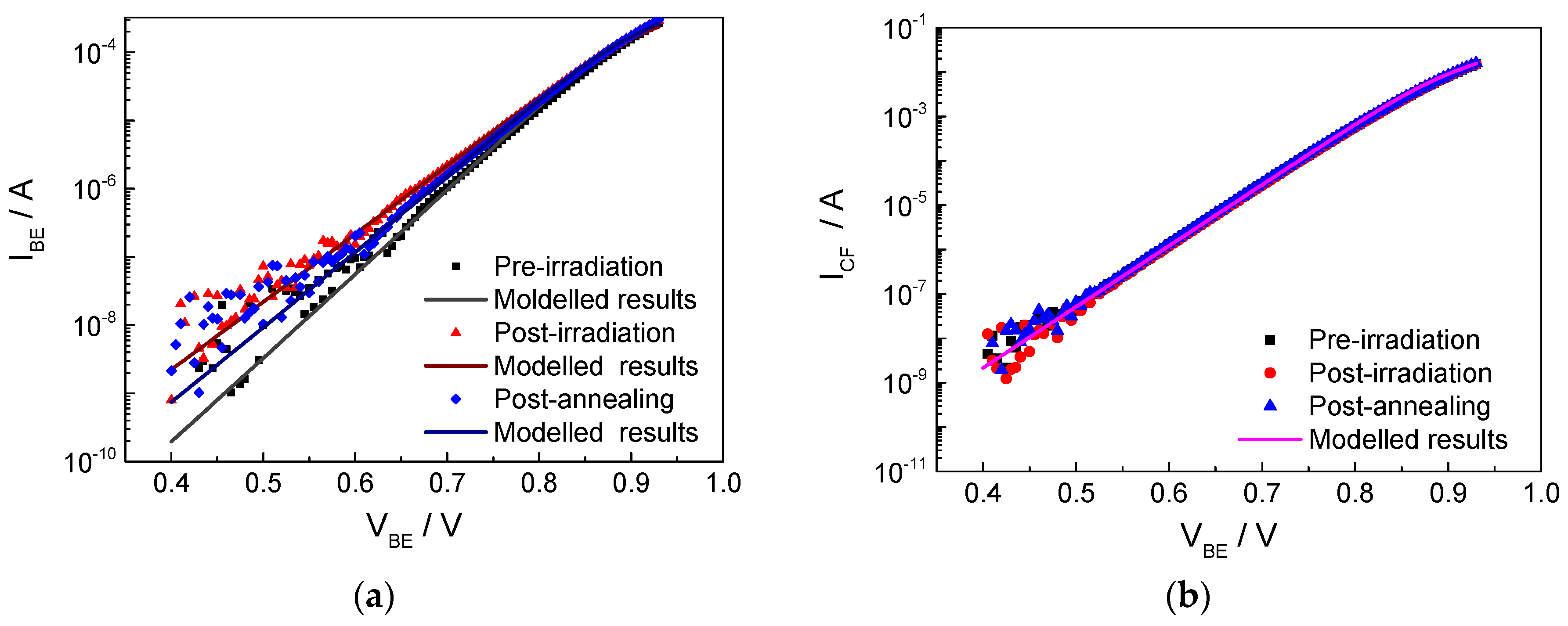
3.1. Forward-Mode Gummel Characteristics

The forward-mode Gummel characteristic, an essential input electrical property of bipolar transistors, effectively reflects the properties of the base–emitter (BE) junction. Figure 3a,b show the measured and modelled base and collector currents for the pre-irradiation, post-irradiation and post-annealing stages, with base and collector voltage varying from 0.4 V to 0.9 V. The base and collector current curves are discrete in the low-voltage range due to the electromagnetic interference, vibration, and temperature disturbance. After irradiation, the collector currents remain relatively stable, while the base currents show a significant increase, particularly noticeable when VBE is below 0.75 V.
In the Agilent HBT model, the collector current ICF in the forward-mode Gummel characteristic is expressed in Equation (1).
I CF = I S × ( exp ( q V BEi N F × k × T ) 1 )
where the parameters Is and NF are the collector saturation current and ideality factor, respectively, which can be obtained from the intercept and slope of the current curves. In addition, k is the Boltzmann constant, T is the temperature, VBEi is the voltage applied to the BE junction, and q is the electron charge.
The base–emitter current IBE is given by Equation (2).
I BE = q 3 mod G K D C × I SH ( exp ( q V BEi N H × k × T ) 1 ) + I SE ( exp ( q V BEi N E × k × T ) 1 )
where the parameters ISH and NH are the base–emitter saturation current and ideality factor in the ideal region (the high-voltage region), respectively, while the parameters ISE and NE are the base–emitter saturation current and ideality factor in the non-ideal region (the low-voltage region), respectively. The method of extracting the model parameters is similar to that of the collector current. The q3mod is an empirical parameter used to model a potential rise in the base current caused by the soft-knee effect. Since this phenomenon is not observed in the measured InP HBTs, the GKDC parameter is set to its default value of 0 [22]. The model parameters of forward Gummel characteristics are extracted and presented in Table 1. As shown in Figure 3, the modelled results demonstrate good agreement with the measured results across a wide voltage range, confirming the effectiveness of the extracted parameters.
In the BE junction, when both the base and collector voltages vary from 0.4 to 0.9 V simultaneously, the BE junction is forward biased while the BC junction is always zero biased. At low voltages, the BE junction is weakly forward biased, causing a small number of electrons diffusing from the emitter region to the base region to spend more time in the space charge region (SCR). This results in the base current at low voltages being primarily dominated by the recombination current in the SCR, which could be characterised by the model parameters ISE and NE. Furthermore, proton irradiation could exacerbate the non-ideal current behaviour shown in Figure 3a. As with the previous analysis in Ref. [8], the interaction of protons with material atoms in InP HBT generates acceptor traps of In vacancies, which act as recombination centres. These traps could reduce the lifetime of minority carriers and increase the recombination rate in devices. As shown in Table 1, the parameter with maximum VR is ISE, which indicates that a large number of irradiation defects are induced in the BE junction and on the InGaAs surface near the base region. Moreover, the value of Ne is generally between 1 and 2, which could characterise the property of recombination current in the SCR. A value of Ne closer to 2 indicates a higher recombination current. When compared to the parameters NF and NH, a higher NE suggests that the irradiation-induced defects lead to a significant recombination current in the SCR of the BE junction. It is most likely associated with the effect of trap-assisted tunnelling in the SCR and the formation of a surface channel near the base region. The band diagram under forward bias, as shown in Figure 4, is used to analyse the conduction mechanism of the BE junction. Irradiation-induced defects in the SCR of the BE junction not only contribute to the diffusion current and the hot carrier emission current but also directly participate in tunnelling process.
In the high-voltage region, the BE junction is strongly forward biased, resulting in a narrow space charge region (SCR). Consequently, the recombination current in the SCR of the BE junction can be disregarded. A large number of electrons diffuse from the emitter region to the base region. Some of these electrons recombine with holes in the quasi-neutral bulk base region (NBR), generating the recombination current, while the remaining electrons diffuse to the collector region boundary and are collected by the BC junction. Therefore, the recombination current in the NBR dominates the base current in the high-voltage region, which can be modelled using the parameters ISH and NH. In Table 1, the middle VR appearing in ISH and NH suggests that there is a minor amount of displacement damage induced by proton irradiation in the bulk base region compared to that induced in the SCR, resulting in a slight increase in the recombination current in the high-voltage region.
Based on the analysis of the base current, the increase in recombination current in the base region would theoretically cause a decrease in the total number of carriers collected by BC junction. However, this decrease is not clearly discernible in Figure 3b. Nevertheless, when examining the model parameters extracted in Table 1, it is found that the negative value of VR of collector saturation current IS implies a minor reduction in the collector current. Furthermore, the minimal VRs of collector saturation current IS and ideality factor NF indicate that the collection charge capability of BC junction is nearly saturated, with the collector current being marginally influenced by proton irradiation. Therefore, it is evident that the model parameters offer a more detailed insight into the effects of irradiation on the devices.
After annealing, the VRs of the parameters decrease significantly compared to the post-irradiation stage. This suggests that some defects generated by displacement damage are recombined after a period of annealing, leading to a slight recovery of the degraded characteristics. However, the remaining defects form stable traps that will have a long-term impact on the DC and AC characteristics of the device. Therefore, the degraded characteristics of post-annealing do not fully recover to the pre-irradiation state.
The current gain (β = ICF/IBE) of the InP HBT is shown in Figure 5. It is evident that the gain decreases after irradiation, which is also attributed to the increase in the recombination current of the BE junction induced by irradiation damage.

3.2. Reserve-Mode Gummel Characteristics

For NPN bipolar transistors, the electrical property of BC junction can be reflected by the reverse-mode Gummel characteristic. The measured and modelled results for pre-irradiation, post-irradiation, and post-annealing with the collector voltage varying from −0.2 V to −0.8 V, and the emitter and base electrodes grounded are shown in Figure 6a,b. The good agreement between the modelled results and experimental data across a wide range in Figure 6 confirms the accuracy of the extracted parameters.
In the compact model, the reverse collector current ICR and base current IBC are expressed in Equations (3) and (4), respectively.
I CR = I SR × ( exp ( q V BCi N R × k × T ) 1 )
I BC = I SRH ( exp ( q V BCi N RH × k × T ) 1 ) + I S C ( exp ( q V BCi N C × k × T ) 1 )
where the parameters include the collector saturation current ISR, ideality factor NR, base–collector saturation current IRSH, ideality factor NRH in the ideal region, as well as the base–collector saturation current ISC and ideality factor NC in the non-ideal region. VBCi stands for the applied voltage of BC junction. The saturation current and the ideality factor parameters are extracted from the intercept and slope of the different regions, as shown in Table 2.
In the reverse-mode Gummel characteristics, as the collector voltage varies from −0.2 to −0.8 V, the BC junction is forward biased while the BE junction is zero biased. Similar to the base current IBE in forward-mode Gummel characteristics, the base current IBC in the reverse characteristics is primarily determined by the recombination current in the space charge region of the BC junction (which can be characterised by parameters ISC and NC) and the recombination current in the quasi-neutral bulk base region (related to IRSH and NRH). As seen in Table 2, the VRs of the model parameters are all zero in the reverse Gummel characteristics, indicating a minimal impact of proton irradiation on the BC junction. This implies that the displacement damage induced in the SCR of the BC junction can be disregarded.
As the voltage of BC junction increases, the collector and base currents gradually saturate, which is attributed to the collector resistance caused by the low doping of the collector region. The voltage drop across the collector resistance in the high-voltage region limits the increase in current, known as the high-level injection effect. Compared to the pre-irradiation and post-annealing state, both the base and collector current decrease slightly after irradiation in the high-voltage region, which may be associated with the collector resistance.
In the model, the extrinsic emitter resistance RE, base resistance RBX and collector resistance RCX can be determined using the Open-Collector method, which involves extrapolating the curves of the real part of the Z-parameters as expressed in Equations (5)–(7) [29,30]. The intrinsic resistance RCI, RBI, along with the thermal resistance, can be obtained from fitting the output characteristics in Figure 7.
R b x = r e a l ( Z 11 Z 12 ) 1 / I b 0
R e = r e a l ( Z 12 ) 1 / I b 0
R c x = r e a l ( Z 22 Z 21 ) 1 / I b 0
As shown in Table 3, the intrinsic and extrinsic collector resistances RCI and RCX show the most significant changes compared to the other resistances with rates of 4.78% and 25.77%, respectively. Due to its large area and low doping, the collector region is susceptible to proton irradiation. As a result, irradiation-induced damage results in a slight increase in the collector resistance in the quasi-neutral bulk collector region. Therefore, due to the effect of the high-level injection, the increased collector resistance is responsible for the slight decrease in base and collector current in the high-voltage region after irradiation, as shown in Figure 6.
Figure 7 shows the comparison between measured and modelled output characteristics at base currents of 20 µA, 40 µA, 60 µA, and 80 µA for pre-irradiation, post-irradiation, and post-annealing, respectively. The strong consistency between measured and modelled results, with an error within 5%, validates the accuracy of the DC model and also demonstrates the effectiveness of the analysis. Moreover, at a fixed base current, the increased carrier recombination in the base region due to irradiation damage results in fewer carriers being collected by the BC junction. Consequently, the collector current decreases after irradiation, with the model parameter analysis of the forward Gummel characteristics.

3.3. Capacitance Characteristics

The characteristics of the defects can also be evaluated by observing their influence on the capacitance. When the BE and BC junction are reverse biased or weakly positive biased (with the base voltage varying from −3 V to 0.4 V), the S-parameters are measured. Then, the junction capacitance can be calculated from the imaginary part of the Y-parameters (converted from S-parameters) in Equations (8) and (9) [31,32].
C b e = i m a g ( Y 11 + Y 12 ) ω
C b c = i m a g ( Y 12 ) ω
Figure 8a,b show the capacitance of the base–emitter junction (CBE) and base–collector junction (CBC) before irradiation, after irradiation, and after annealing. The great agreement between the measured and modelled results for both the BE and BC junctions confirms the accuracy of the extracted model parameters. As shown in Figure 8, the CBE increases after irradiation and then decreases slightly after annealing, while the CBC is hardly affected by proton irradiation. This differs from the capacitance behaviour of InP HBT under gamma irradiation, as reported in Reference [22], where both CBE and CBC show an increase.
In the compact model, the equations for the junction capacitances can be found in the Reference [28]. CBE is characterised by several parameters, namely the zero-biased capacitance Cje, maximum value in forward bias Cemax, built-in voltage Vje, grading factor Mje, punch-through voltage Vpte, and grading factor beyond punch-through Mjer. Similarly, CBC also has analogous parameters, including Cjc, Ccmax, Vjc, Mjc, Vptc and Mjcr, which are listed in Table 4.
Apart from Cje and Mjer, no changes were observed in the other parameters. This implies that the irradiation-induced degradation mainly takes place in the BE junction rather than the BC junction, which is consistent with the analysis of the parameters in the forward and reverse Gummel characteristics. In the BE junction, the defects induced by proton irradiation could capture or release carriers with the changes in applied voltage, which is equivalent to the effect of charging or discharging, thus resulting in an increase in CBE after irradiation [33]. Furthermore, the absolute rate of VR for Mjer is higher compared to Cje. Mjer, defined as the grading factor beyond punch-through, is the parameter that describes the slope of the punch-through region for the base–emitter junction. It can not only reflect changes of CBE, but is also associated with the tunnel phenomenon, confirming the trap-assisted tunnelling mechanism in the recombination current of the BE junction.
In addition, the VRs of the model parameters decrease after annealing, indicating a recovery of the defects in the BE junction compared to the post-irradiation state. However, this is different from the capacitance property of GaAs HBT under gamma irradiation in Reference [21], where further degradation was reported after annealing compared to the post-irradiation condition.

3.4. Frequency Characteristics

The cut-off frequency (Ft) is the frequency at which the current gain drops to unity in a common-emitter transistor, which is a crucial parameter in characterising the AC performance of high-frequency devices. To determine Ft, the S-parameters and collector current are measured as the base current varies from 10 μA to 150 μA with the collector voltage fixed at 1.7 V. By extrapolating the H(2,1) curves derived from S-parameters at different collector currents, the cut-off frequency can be calculated. The measured and modelled results of the cut-off frequency for pre-irradiation, post-irradiation, and post-annealing are shown in Figure 9a. It is observed that the cut-off frequency exhibits more pronounced variations with increasing collector current.
Actually, the cut-off frequency is primarily determined by the transit time in the devices, as expressed in Equation (10). A longer transit time results in a lower cut-off frequency. The total transit time (τ) is the sum of several individual transit times, including the charging time in the emitter region (τe), the transit time in the base region (τb), the transit time in the depletion region of the BC junction (τsc) and the charging time in the collector region (τc), as described in Equations (11)–(14). The cut-off frequency can be improved effectively by optimising these transit times.
f T = 1 2 π τ = 1 2 π ( τ e + τ b + τ c + τ sc )
τ e = k T q I C ( C BE + C BC )
τ b = T B 2 2 D nB
τ sc = T dep 2 v eff
τ c = ( R E + R C ) · C BC
where T is the temperature, CBE and CBC are the BE and BC junction capacitance, respectively, TB is the thickness of the base region, DNB is the electron diffusion coefficient in the base region, Tdep is the width of the BC junction depletion region, veff is the electron average rate in the depletion region of BC junction, and RE and RC are the emitter and collector resistances, respectively.
Nevertheless, in the compact model, three types of transit time are considered. The base region (τb) and BC junction (τsc) transit time correspond to Equations (12) and (13), respectively. Additionally, if the cut-off frequency decreases at the high current injection, the excess delay due to the Kirk effect (τke) must be considered; otherwise, default parameters would be used. Detailed equations and descriptions of these transit time parameters can be found in Reference [26]. These transit times, along with the transit time caused by capacitance and resistance in Equations (11) and (14), collectively determine the total transit time (τ), as shown in Figure 9b. The error between the measured and modelled results is within 3%, validating the accuracy of the AC model. The extracted model parameters are listed in Table 5.
As seen in Table 5, it is evident that only the base transit time parameter Tfb exhibits significant changes before and after irradiation. For a heavily doped base, it is reasonable to approximate that the transit time in the base region (τb) is a constant at low and medium currents (below Kirk effect), which could be modelled by the parameter Tfb [26]. As analysed in the forward-mode Gummel characteristics, the changes in parameters ISH and NH before and after irradiation suggest that the amount of displacement damage is induced in the quasi-neutral bulk base region (NBR). This could lead to an increased carrier recombination rate and a decreased diffusion coefficient (DNB) in the NBR, resulting in an increase in the base transit time (τb) according to Equation (12). In addition, based on the analysis of reverse-mode characteristics, the impact of proton irradiation on the collector junction can be neglected. Therefore, the VR of the related model parameters (Tfc0, Tcmin, Itc, Itc2, Vtc0lnv, Vtr0, Vmx0 and Vtmin) are zero in Table 5.
Finally, the proton irradiation, the increase in collector resistance, capacitance of the BE junction, as well as the base transit time (τb), collectively result in a reduction in the cut-off frequency.

4. Conclusions

The DC and AC characteristics in InP HBT have been studied and modelled using a compact model for pre-irradiation, post-irradiation, and post-annealing. The degradation mechanism could be reflected by the change in model parameters. In the forward and reverse Gummel characteristics, the parameter with the maximum variation rate is ISE, which is related to the recombination current around the BE junction. It indicates that the space charge region of the BE junction and the InGaAs surface near the base region are more significantly affected by proton irradiation. The change in the ISH and NH parameters before and after irradiation suggests that a minor amount of displacement damage is induced in the quasi-neutral bulk base region (NBR). Based on the previous analysis, acceptor traps of In vacancies are generated by the collision of protons with material atoms, which act as recombination centres and decrease the minority carriers lifetime, resulting in a significant recombination current in the BE junction.
In the AC characteristics, the radiation degradation around the BE junction results in an increase in the CBE and a decrease in the cut-off frequency after irradiation. The variation rate of parameter Mjer validates the trap-assisted tunnelling mechanism in the recombination current of the BE junction. The significant changes in the base region transit time parameter Tfb before and after irradiation are consistent with the analysis of degradation in the quasi-neutral bulk base region (NBR).
After annealing, the variation rates of the parameters decrease significantly, which indicates a reduction in defect density compared to post-irradiation. Some unstable defects in the BE junction are recombined and disappear after a period of annealing, while the remaining stable traps will have a long-term influence on the device characteristics.
Finally, the good agreement between the modelled and measured results of DC and AC characteristics confirms the accuracy and effectiveness of the extracted model parameters. This lays the foundation for the establishment of an irradiation compact model to predict device characteristics and also provides a powerful tool to design anti-radiation circuits in future work.

Author Contributions

Conceptualisation, X.Z.; methodology, X.Z.; software, X.Z.; validation, X.Z.; formal analysis, Y.C.; investigation, S.C.; resources, Y.Z.; data curation, X.W.; visualisation, Y.B. and S.S.; supervision, H.W. and F.P.; project administration, X.Z.; funding acquisition, X.Z.; writing—original draft, X.Z.; writing—review and editing, G.T. and Y.Y. All authors have read and agreed to the published version of the manuscript.

Funding

This research was funded by National Natural Science Foundation of China (Grant No. 62104260).

Data Availability Statement

All the data are shown in the paper.

Acknowledgments

The authors would like to acknowledge the Institute of Microelectronics of the Chinese Academy of Sciences for providing test samples and Institute of Heavy Ion Physics of Peking University for providing experimental equipment.

Conflicts of Interest

Author Shaowei Sun was employed by the company LONGi Green Energy Technology Co., Ltd. The remaining authors declare that the research was conducted in the absence of any commercial or financial relationships that could be construed as a potential conflict of interest.

References

  1. Urteaga, M.; Griffith, Z.; Seo, M.; Hacker, J.; Rodwell, M.J. InP HBT technologies for THz integrated circuits. Proc. IEEE 2017, 105, 1051–1067. [Google Scholar] [CrossRef]
  2. Yun, J.; Oh, S.J.; Song, K.; Yoon, D.; Son, H.Y.; Choi, Y.; Huh, Y.M.; Rieh, J.S. Terahertz reflection-mode biological imaging based on InP HBT source and detector. IEEE Trans. Terahertz Sci. Technol. 2017, 7, 274–283. [Google Scholar] [CrossRef]
  3. Yun, J.; Kim, J.; Rieh, J.S. A 280-GHz 10-dBm Signal Source Based on InP HBT Technology. IEEE Microw. Wirel. Compon. Lett. 2017, 27, 159–161. [Google Scholar] [CrossRef]
  4. Hansen, D.L.; Chu, P.; Meyer, S.F. Effects of data rate and transistor size on single event upset cross-sections for InP-based circuits. IEEE Trans. Nucl. Sci. 2005, 52, 3166–3171. [Google Scholar] [CrossRef]
  5. Hansen, D.L.; Marshall, P.W.; Lopez-Aguado, R.; Jobe, R.K.; Carts, M.A.; Marshall, C.J.; Meyer, S.F. A study of the SEU performance of InP and SiGe shift registers. IEEE Trans. Nucl. Sci. 2005, 52, 1140–1147. [Google Scholar] [CrossRef]
  6. Chu, P.; Hansen, D.L.; Doyle, B.L.; Jobe, K.; Lopez-Aguado, R.; Shoga, M.; Walsh, D.S. Ion-microbeam probe of high-speed shift registers for SEU Analysis-part II: InP. IEEE Trans. Nucl. Sci. 2006, 53, 1583–1592. [Google Scholar] [CrossRef]
  7. Li, C.H.; Lu, H.L.; Zhang, Y.M.; Liu, M.; Zhao, X.H. Proton-Induced Degradation of InP/InGaAs HBTs Predicted by Nonionizing Energy Loss Model. IEEE Trans. Nucl. Sci. 2015, 62, 1336–1340. [Google Scholar] [CrossRef]
  8. Zhao, X.H.; Lu, H.L.; Zhao, M.L.; Zhang, Y.M.; Zhang, Y.M. The Study of Deep Level Traps and Their Influence on Current Characteristics of InP/InGaAs Heterostructures. Nanomaterials 2019, 9, 1141. [Google Scholar] [CrossRef]
  9. Zhao, X.H.; Lu, H.L.; Zhang, Y.M.; Zhang, Y.M.; Wei, Z.C. The impact of laser energy, bias and irradiation positions on single event transients of InP HBT. J. Phys. D Appl. Physic. 2020, 53, 145104. [Google Scholar] [CrossRef]
  10. Wei, J.N.; He, C.H.; Li, P.; Li, Y.H.; Guo, H.X. Impact of displacement damage on single event transient charge collection in SiGe HBTs. Nucl. Instrum. Methods Phys. Res. Sect. A Accel. Spectrometers Detect. Assoc. Equip. 2019, 938, 29–35. [Google Scholar] [CrossRef]
  11. Meng, X.T.; Yang, H.W.; Kang, A.G.; Wang, J.L.; Jia, H.Y.; Chen, P.Y.; Tsien, P.H. Effects of neutron irradiation on SiGe HBT and Si BJT devices. J. Mater. Sci. Mater. Electron. 2003, 14, 199–203. [Google Scholar] [CrossRef]
  12. Petrosyants, K.; Vologdin, E.; Smirnov, D.; Torgovnikov, R.; Kozhukhov, M. Si BJT and SiGe HBT performance modeling after neutron radiation exposure. In Proceedings of the 2011 9th East-West Design & Test Symposium (EWDTS), Sevastopol, Ukraine, 9–12 September 2011; pp. 267–270. [Google Scholar]
  13. Zhang, X.; Li, Y.; Guo, Q.; Feng, J. Low energy proton irradiation effects on InP/InGaAs DHBTs and InP-base frequency dividers. Young Sci. Forum 2017, 10710, 65–70. [Google Scholar]
  14. Zhang, X.Y.; Zhang, X.; Li, Y.; Guo, Q.; Liao, B.; Yang, S.; Yang, Z.; He, C. Displacement damage effects and anneal characteristic on InP/InGaAs DHBTs. In Proceedings of the 2018 International Conference on Radiation Effects of Electronic Devices (ICREED), Beijing, China, 16–18 May 2018; pp. 1–5. [Google Scholar]
  15. Lawal, O.M.; Liu, S.; Huang, T. Extraction and analysis of gamma irradiated Si BJT SPICE model. ECS J. Solid State Sci. Technol. 2019, 8, 51. [Google Scholar] [CrossRef]
  16. Petrosyants, K.O.; Kozhukhov, M.V.; Dvomikov, O.V.; Savchenko, E.M.; Budyakov, A.S. SPICE-model of SiGe HBT taking into account radiation effects. In Proceedings of the 2018 Moscow Workshop on Electronic and Networking Technologies (MWENT), Moscow, Russia, 14–16 March 2018; pp. 1–4. [Google Scholar]
  17. Petrosyants, K.O.; Kozhukhov, M.V. TCAD-SPICE Two Level Simulation of Si BJTs and SiGe HBTs Taking into Account Radiation Effects. Dev. Issues Adv. Microelectron. Nanoelectron. Syst. (MES) 2017, 2, 2–10. [Google Scholar]
  18. Petrosyants, K.; Kozhukhov, M. SPICE model parameters extraction taking into account the ionizing radiation effects. In Proceedings of the 2014 Proceedings of IEEE East-West Design & Test Symposium, Kiev, Ukraine, 26–29 September 2014; pp. 1–4.
  19. Van Uffelen, M.; Geboers, S.; Leroux, P.; Berghmans, F. SPICE modelling of a discrete COTS SiGe HBT for digital applications up to MGy dose levels. In Proceedings of the 2005 8th European Conference on Radiation and Its Effects on Components and Systems, Cap d’Agde, France, 19–23 September 2005; pp. PF4-1–PF4-5. [Google Scholar]
  20. Zhang, J.; Zhang, Y.; Lu, H.; Zhang, Y.; Yang, S. The model parameter extraction and simulation for the effects of gamma irradiation on the DC characteristics of InGaP/GaAs single heterojunction bipolar transistors. Microelectron. Reliab. 2012, 52, 2941–2947. [Google Scholar] [CrossRef]
  21. Zhang, J.; Xu, K.; Wang, J.; Liu, M.; Zhang, L.; Liu, B. Modeling and analysis for the effects of gamma irradiation on the DC and AC performance in InGaP/GaAs SHBTs. Radiat. Eff. Defects Solids 2020, 175, 492–503. [Google Scholar] [CrossRef]
  22. Zhang, J.; Cao, L.; Liu, M.; Liu, B.; Cheng, L. Gamma-induced degradation effect of InP HBTs studied by Keysight model. Nucl. Sci. Eng. 2021, 195, 173–184. [Google Scholar] [CrossRef]
  23. Jin, Z.; Su, Y.B.; Cheng, W.; Liu, X.Y.; Xu, A.H.; Qi, M. High current multi-finger InGaAs/InP double heterojunction bipolar transistor with the maximum oscillation frequency 253 GHz. Chin. Phys. Lett. 2008, 25, 3075–3078. [Google Scholar]
  24. Zhang, J.C.; Liu, M.; Wang, J.; Zhang, L.; Liu, B. Modeling of InP HBTs with an Improved Keysight HBT Model. Microw. J. 2019, 62, 56. [Google Scholar]
  25. Zhang, A.; Gao, J. An improved nonlinear model for millimeter-wave inp hbt including dc/ac dispersion effects. IEEE Microw. Wirel. Compon. Lett. 2021, 99, 465–468. [Google Scholar] [CrossRef]
  26. Iwamoto, M.; Root, D.E.; Scott, J.B.; Cognata, A.; Asbeck, P.M.; Hughes, B.; D’Avanzo, D.C. Large-signal HBT model with improved collector transit time formulation for GaAs and InP technologies. In Proceedings of the IEEE MTT-S International Microwave Symposium Digest, Philadelphia, PA, USA, 8–13 June 2003; Volume 2, pp. 635–638. [Google Scholar]
  27. Johansen, T.K.; Midili, V.; Squartecchia, M.; Zhurbenko, V.; Nodjiadjim, V.; Dupuy, J.Y.; Riet, M.; Konczykowska, A. Large-Signal Modeling of Multi-Finger InP DHBT Devices at Millimeter-Wave Frequencies. In Proceedings of the International Workshop on Integrated Nonlinear Microwave and mmWave Circuits, Graz, Austria, 20–21 April 2017; pp. 1–3. [Google Scholar]
  28. UCSD HBT Model. Available online: http://hbt.ucsd.edu (accessed on 1 December 2023).
  29. Wei, C.J.; Hwang, J.C.M. Direct extraction of equivalent circuit parameters for heterojunction bipolar transistors. IEEE Trans. Microw. Theory Tech. 1995, 43, 2035–2040. [Google Scholar]
  30. Bousnina, S.; Mandeville, P.; Kouki, A.B.; Surridge, R.; Ghannouchi, F.M. Direct parameter-extraction method for HBT small-signal model. IEEE Trans. Microw. Theory Tech. 2002, 50, 529–536. [Google Scholar] [CrossRef]
  31. Lee, K.; Choi, K.; Kook, S.H.; Cho, D.H.; Park, K.W.; Kim, B. Direct parameter extraction of SiGe HBTs for the VBIC bipolar compact model. IEEE Trans. Electron Devices 2005, 52, 375–384. [Google Scholar] [CrossRef]
  32. Samelis, A.; Pavlidis, D. DC to high-frequency HBT-model parameter evaluation using impedance block conditioned optimization. IEEE Trans. Microw. Theory Tech. 1997, 45, 886–897. [Google Scholar] [CrossRef]
  33. Zhao, X.H.; Lu, H.L.; Zhang, Y.M.; Zhang, Y.M. Impact of proton irradiation with different fluences on the characteristics of InP/InGaAs heterostructure. Radiat. Eff. Defects Solids 2019, 174, 697–707. [Google Scholar] [CrossRef]
Figure 1. The structure diagram of InP/InGaAs HBT. (a) The doping and thickness of layers. (b) The process technology (The red, green, and blue regions are emitter, base, and collector ohmic contacts, respectively. The yellow area is the metal deposited so that the electrodes are at the same height).
Electronics 13 01831 g001
Figure 2. The Agilent HBT model without the parasitic elements.
Electronics 13 01831 g002
Figure 3. Measured and modelled forward-mode Gummel characteristics for pre-irradiation, post-irradiation and post-annealing of 10 MeV (proton). (a) Base current. (b) Collector current.
Electronics 13 01831 g003
Figure 4. The band diagrams under forward bias (The green symbols represents electrons).
Electronics 13 01831 g004
Figure 5. Current gain (β) for pre-irradiation, post-irradiation, and post-annealing of 10 MeV (proton).
Electronics 13 01831 g005
Figure 6. Measured and modelled reverse-mode Gummel characteristic for pre-irradiation, post-irradiation, and post-annealing of 10 MeV (proton). (a) Collector current. (b) Base current.
Electronics 13 01831 g006
Figure 7. Measured and modelled output characteristics before irradiation, after irradiation, and after annealing of 10 MeV (proton).
Electronics 13 01831 g007
Figure 8. Measured and modelled base–emitter and base–collector junction capacitance for pre-irradiation, post-irradiation, and post-annealing. (a) BE junction capacitance (CBE); (b) BC junction capacitance (CBC).
Electronics 13 01831 g008
Figure 9. Measured and modelled results for pre-irradiation, post-irradiation, and post-annealing of 10 MeV (proton). (a) Cut-off frequency (Ft). (b) Transit time (τ).
Electronics 13 01831 g009
Table 1. The current parameters of forward-mode Gummel characteristics for pre-irradiation, post-irradiation, and post-annealing.
Pre-IrradiationPost-IrradiationVRPost-AnnealingVR
IS (A)6.83 × 10−156.80 × 10⁻¹⁵−0.44%6.81 × 10⁻¹⁵−0.31%
NF1.221.230.82%1.220
ISH (A)2.41 × 10−163.00 × 10−1624.48%2.20 × 10⁻¹⁶−8.71%
NH1.291.354.65%1.300.77%
ISE (A)2.45 × 10−152.50 × 10−1310,104.08%3.30 × 10−141246.94%
NE1.411.7121.28%1.5610.64%
Table 2. The current parameters of reverse-mode Gummel characteristics for pre-irradiation, post-irradiation, and post-annealing.
Pre-IrradiationPost-IrradiationVRPost-AnnealingVR
ISR (A)2.47 × 10−122.47 × 10−1202.47 × 10−120
NR1.201.2001.200
ISRH (A)6.72 × 10−166.72 × 10−1606.72 × 10−160
NRH1.031.0301.030
ISC (A)2.49 × 10−112.49 × 10−1102.49 × 10−110
NC1.311.3101.310
Table 3. The resistance parameters of resistances for pre-irradiation, post-irradiation, and post-annealing.
Pre-IrradiationPost-IrradiationVRPost-AnnealingVR
RBX (Ω)0.310.323.22%0.310
RBI (Ω)0.10.100.10
RE (Ω)2.12.102.10
RCX (Ω)3.884.8825.77%3.880
RCI (Ω)2.092.194.78%2.090
Rth1 (Ω)0.10.100.10
Rth2 (Ω)0.10.100.10
Table 4. The capacitance parameters for pre-irradiation, post-irradiation, and post-annealing.
Pre-IrradiationPost-IrradiationVRPost-AnnealingVR
Cje (F)1.672 × 10−141.677 × 10−140.3%1.674 × 10−140.12%
Cemax (F)6.06 × 10−146.06 × 10−1406.06 × 10−140
Vje (V)0.64 V0.64 V00.64 V0
Mje0.780.7800.780
Vpte0.110.1100.110
Mjer0.0700.067−4.28%0.068−2.94%
Cjc (F)1.35 × 10−131.35 × 10−1301.35 × 10−130
Ccmax (F)2.01 × 10−132.01 × 10−1302.01 × 10−130
Vjc (V)0.67 V0.67 V00.67 V0
Mjc0.960.9600.960
Vptc2.222.2202.220
Mjcr0.010.0100.010
Table 5. The transit time parameters for pre-irradiation, post-irradiation, and post-annealing.
Pre-IrradiationPost-IrradiationVRPost-AnnealingVR
Tfb (S)4.60 × 10−135.40 × 10−1317.4%5.10 × 10−1310.9%
Tfc0 (S)1.33 × 10−111.33 × 10−1101.33 × 10−110
Tcmin (S)3.20 × 10−143.20 × 10−1403.20 × 10−140
Itc (A)7.60 × 10−47.60 × 10−407.60 × 10−40
Itc2 (A)7 × 10−47 × 10−407 × 10−40
Vtc0lnv33030
Vtr0 (V)22020
Vmx0 (V)0.50.500.50
Vtmin (V)1.21.201.20
Disclaimer/Publisher’s Note: The statements, opinions and data contained in all publications are solely those of the individual author(s) and contributor(s) and not of MDPI and/or the editor(s). MDPI and/or the editor(s) disclaim responsibility for any injury to people or property resulting from any ideas, methods, instructions or products referred to in the content.

