Article

Modeling and Mitigating Output-Dependent Modulation in Current-Steering DAC Based on Differential-Quad Switching Scheme

1
State Key Laboratory of Materials for Integrated Circuits, Shanghai Institute of Microsystem and Information Technology, Chinese Academy of Sciences, Shanghai 200050, China
2
University of Chinese Academy of Sciences, Beijing 100049, China
3
Center of Materials Science and Optoelectronics Engineering, University of Chinese Academy of Sciences, Beijing 100049, China
*
Author to whom correspondence should be addressed.
Electronics 2024, 13(10), 1992; https://doi.org/10.3390/electronics13101992
Submission received: 15 April 2024 / Revised: 13 May 2024 / Accepted: 16 May 2024 / Published: 20 May 2024
(This article belongs to the Special Issue Advanced Analog and Mixed-Mode Integrated Circuits)

Abstract

:
This brief presents a comprehensive analysis of the output-dependent modulation (ODM) in a current-steering digital-to-analog converter (CS-DAC) based on the differential-quad switching (DQS) structure. A mathematical model is proposed to accurately describe ODM, which is categorized into two types: output transition errors and boundary effect errors. A novel approach of adding isolation devices is introduced and reinterpreted to mitigate the effect of ODM. The simulation results indicate that the inclusion of isolation devices efficiently suppresses the odd harmonics at mid-to-high frequency by a value that is 13 dB lower than before. Experimental validation is conducted on a 16-bit 250 MS/s CS-DAC fabricated in a 180 nm process.

1. Introduction

CS-DACs have been widely used in wireless communication systems for their excellent speed performance. The dynamic performance of CS-DACs, particularly the SFDR, has attracted significant attention in engineering. Prior works [1,2,3] have developed analytical models and examined the relationship between the SFDR and output impedance. However, high-speed DACs may still experience performance degradation when converting high-frequency signals, even with ideal current sources.
Currently, various techniques have been proposed to enhance the SFDR, including dynamic element matching (DEM) [4,5,6], differential-quad switching (DQS) [7,8,9], and the combination of these approaches [10,11]. The DEM technique eliminates the mapping between the digital input code and the corresponding current elements of DAC, minimizing the impact of mismatch between current elements on the SFDR. Nevertheless, studies have shown that DACs still suffer from harmonic distortion with the DEM scheme [12], as they are also affected by output-dependent modulation (ODM). Conventional DEM only deals with mismatches of an individual DAC; a new time-interleaving DEM (T-DEM) that randomizes the residual offset, gain, and skew mismatches is introduced in [13]. T-DEM tackles the mismatches between the two DACs, reducing the constraint of TI spur on the performance of high-speed TI DACs.
The DQS structure, first introduced in [7], eliminates the code-dependent distortion by incorporating a pair of complementary switches. Similarly, the switching process in the DQS structure is also modulated by the output signal, and the mismatch between switches can deteriorate the dynamic performance of DACs [11]. Work [10] applies the novel grouped random rotation thermometer code (GRTC) and differential-quad switching (DQS) and has good dynamic performance without calibrations. This is because the GRTC suppresses the harmonics caused by element mismatches, while the DQS reduces the output-dependent distortion to achieve a high SFDR. The GRTC relies on intricate digital logic for its implementation, and its design challenges and performance are closely linked to the segmentation method of DACs.
Up to now, many novel calibration schemes and circuit structures have been proposed to improve the linearity and dynamic performance of DACs. Work [14] presents a Nyquist-rate CS-DAC that achieves a peak SFDR of better than 87 dB, which is enabled by a fully integrated digital calibration technique that measures and cancels both static and dynamic mismatch errors over the first Nyquist band.
In [15,16], a switching-glitch compensation (SGC) technique greatly reduced the code-dependent switching glitch effect: thus, the SFDR performance at high Fout is improved. The SGC is realized with glitch duplicators and is proposed to generate a complementary amount of switching glitch at the DAC output, which results in significant area consumption. An output impedance compensation (OIC) technique [17] using a compensation resistor, implemented by a PMOS with code-dependent gate voltage control, is proposed to remedy the nonlinearity induced by the insufficient output impedance of the non-cascoded current cells. The DAC achieves > 65 dBc SFDR over the entire Nyquist bandwidth at 10 GS/s. While the circuit structure of this technology is simple, it requires ingenious design, which often leads to an increase in certain costs.
To mitigate the effects of ODM, a new theoretical model for describing ODM is introduced and validated. Additionally, an approach utilizing isolation devices is suggested in this brief, which can reduce output-dependent errors by a factor of 4–5 and maximize the reduction of third harmonic components at high signal frequencies by 13 dB, significantly improving the SFDR of DACs based on the DQS structure.
The structure of this brief is as follows: Section 2 analyzes the mechanism of ODM in DQS-based DACs and presents the harmonic analysis model. Section 3 outlines the CS-DAC architecture and the circuit implementations. Section 4 reports the measured results. The conclusion is drawn in Section 5.

2. Output-Dependent Modulation Based on DQS Structure

The circuit and timing sequence of DQS structure are depicted in Figure 1. In terms of the number of switches, the DQS structure consists of four switches, while the normal structure only has two switches. The typical feature of the DQS structure is that during each conversion, only one pair of switches undergoes switching in a single switched current source. The DQS structure effectively eliminates code-dependent distortion, but ODM that can compromise the system’s dynamic performance remains. In this brief, ODM mainly involves two types of errors: those caused by output transition as well as the different output boundaries before and after conversion.
This section presents a comprehensive model of ODM utilizing a seven-bit DQS-based CS-DAC with a full temperature encoder. The model can be easily extended to various DACs encoded in binary as well as hybrid encoding.

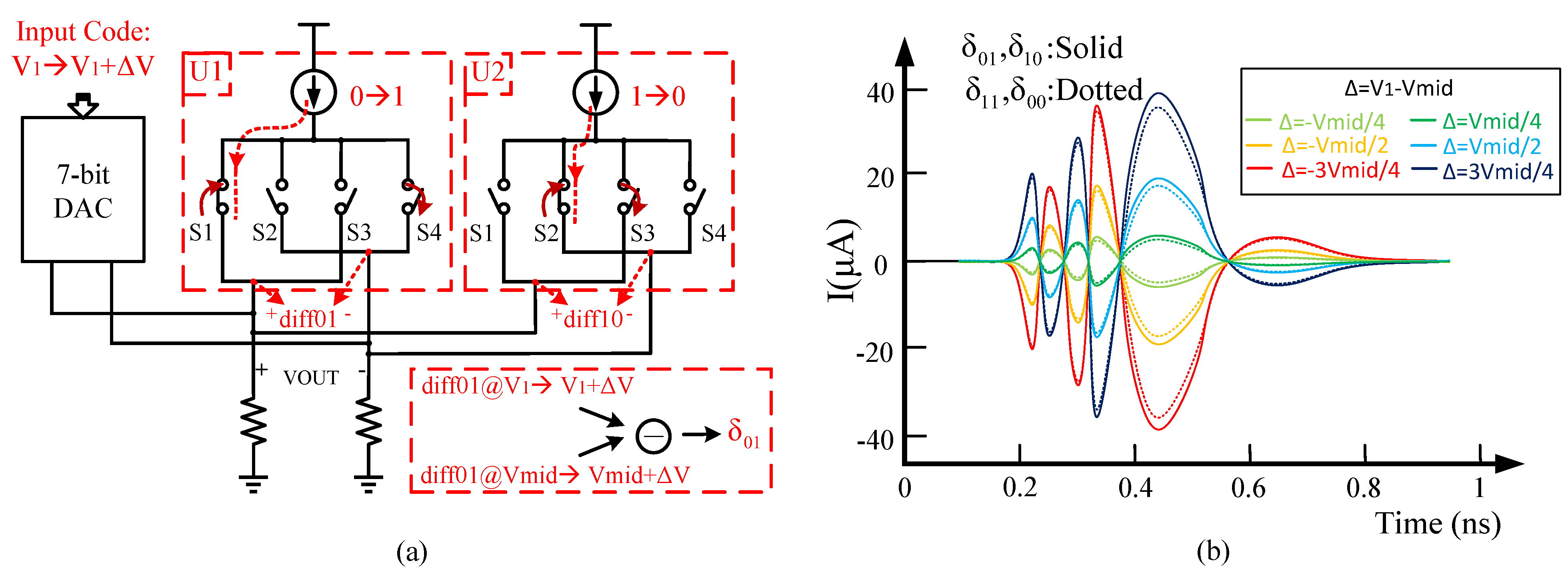
2.1. Opposite-Side Switching Errors (OSEs)

With the circuit configuration mentioned in [12], this work initially investigates the switching distortion caused by output transition through SPICE simulation. As shown in Figure 2a, for transitions from zero to one (U1: S1 or S3 is on, S2 or S4 is off) and from one to zero (U2: S1 or S3 is off, S2 or S4 is on), we define the differences in output current between the unit with output transition and the unit without it as δ 01 and δ 10, respectively, representing the switching errors on opposite sides.
For transitions from one to one (S1 and S3 alternate conducting, S2 and S4 are always off) and from zero to zero (S1 and S3 are always off, S2 and S4 alternate conducting), similarly, the corresponding differences can be expressed as δ 11 and δ 00, respectively, representing the switching errors on same side.
For the code transition from V 1 to V 2 , we set:
V 1 = V m i d
where V m i d denotes the value of middle code of the input sequence. Specifically, for a seven-bit DAC, the value of V m i d is equivalent to 64 (b’1000000).
During each conversion, both δ 01 and δ 10 exhibit the same multiplicative effect with the magnitude of output transition Δ V ( Δ V = V 2 V 1 ), as illustrated in Figure 2b. However, there is a slight difference between them, and the waveform of δ 01– δ 10 is in the inset. The error is independent of the transition direction and can be represented by an even function f Δ V . Its size increases with the absolute value of Δ V , but it is not a simple linear relationship. Due to its relatively low energy, the tiny errors cannot be considered as a major source of distortion.
To facilitate analysis of switching errors, we summarize a general model by directly correlating the switching events with the OSEs. Before analyzing the impact of OSEs on SFDR, the following assumptions are necessary:
(1)
Assume that δ 11 ( δ 00) and δ 01 ( δ 10) have the same output dependency.
(2)
Ignore the influence of initial and final output voltages on errors; the OSEs are solely related to output transition.
During each conversion from V 1 to V 2 , the total number of switching events is equal to the current elements’ number, defined as N. The OSEs are completely opposed to each other under the constant Δ V conditions, as follows:
δ 01 V m i d , V m i d + Δ V = δ 10 V m i d , V m i d Δ V
Thus, the OSEs can be expressed as follows:
δ 01 = δ 11 = ε O 1 · Δ V + f Δ V 2
δ 10 = δ 00 = ε O 1 · Δ V f Δ V 2
where ε O 1 represents the unit switching error when the output increases by 1 LSB, and Δ V denotes the amplitude of the output transition. In a DQS structure, the distortion introduced by OSEs can be expressed as:
E r r O S 1 = V 1 δ 11 + N V 2 δ 00 + Δ V δ 01 , i f V 1 < V 2
E r r O S 2 = V 2 δ 11 + N V 1 δ 00 Δ V δ 10 , i f V 1 > V 2
Based on (1)–(6), it can be proved that (Details are provided in Appendix A):
E r r O S , D Q S = E r r O S 1 = E r r O S 2 = V 2 N 2 · f Δ V + ε O 1 · N V 2 V 1
Clearly, the first term of Equation (7) contains third harmonic components. If the input signal contains the offset error, even harmonics will emerge, which is consistent with the conclusion in work [12]. And the unit switching error ε O 1 pertaining to OSEs does not introduce harmonic components.
In a normal structure, the distortion introduced by OSEs can be expressed as:
E r r O S , N O R = q · V 2 N 2 2 ε O 1 + V 2 N 2 · f Δ V 2
where aiming for simplicity, q is introduced:
q t = V 2 V 1 V 2 V 1
Compared with the DQS structure, the first term of Equation (8) shows that the normal structure is affected by OSEs, leading to the incorporation of additional odd harmonics. Therefore, the DQS structure exhibits better dynamic performance, which is attributed to the code independence of the DQS structure itself.

2.2. Same-Side Switching Errors (SSEs)

Actually, Assumption (1) in Section 2.1 is invalid due to the distinct external environments of the opposite-side switches and the same-side switches, i.e., δ 11 ≠ δ 01, δ 00 ≠ δ 10. It is expected that they will exhibit varying impacts from the output transition. The opposite-side switching can be transformed into the same-side switching by modifying the switch logic of U1 and U2 to direct current towards the same resistor. Subsequently, the SSEs δ 11 and δ 00 can be obtained under the initial condition V 1 = V m i d .
Figure 3 illustrates the differences between the OSEs and SSEs under the same Δ V , i.e., δ 00– δ 10 and δ 11– δ 01, whose magnitudes are directly proportional to Δ V and whose signs follow the direction of Δ V . Therefore, the SSEs in (3) and (4) can be reformulated as:
δ 11 = δ 01 + ε O 2 · Δ V
δ 00 = δ 10 + ε O 2 · Δ V
where ε O 2 represents δ 00– δ 10 and δ 11– δ 01 when the output increases by 1 LSB.
Rewriting (7), E r r O , S includes the effects of both OSEs and SSEs:
E r r O , S , D Q S = V 2 N 2 · f Δ V q · ε O 2 V 2 V 1 2 + ε O 1 + ε O 2 · N V 2 V 1
As we can see from (12), one of the primary sources of odd harmonics in the DQS structure is ε O 2 , the difference between SSEs and OSEs. By substituting the sine input signals V 1 = N 2 s i n w t + N 2 , V 2 = N 2 s i n w t + T s + N 2 into the second term, we can derive the third harmonic distortion; the remaining odd-order components are too minor to be considered significant:
H D 3 = 4 N 2 1 c o s w T s ε O 2 15 π · c o s 3 w t + T s 2
When ε O 2 doubles, HD3 increases by 6 dB in a DQS structure. However, for the normal structure of a current element with a pair of switches, ε O 1 s are the primary sources of distortion. Ultimately, this difference leads to the DAC with the DQS structure being less affected by ODM.
Through MATLAB simulation, the influence of output transition on the SFDR of a full thermometer-coded 16-bit DAC with a normal structure can be obtained under different output signal frequencies, as shown in Figure 4.
Figure 4a depicts the DAC spectrum with the introduction of OSEs due to output transitions when the input signal frequency is 41MHz. It can be observed that there are distinct third harmonics present. Figure 4b illustrates the curve of the DAC’s SFDR varying with the output signal frequency under the condition of N ε O 1 = 5 × 10 8 . In practical circuit design, due to the low amplitude limit, it is difficult to directly observe the unit error. However, the error waveform can be obtained through simulation utilizing the property of the output transition error being related to Δ V .

2.3. Boundary Effect Errors (BEEs)

Except for output transition, the ODM also includes the influence of output voltages before and after the conversion, that is, the boundary effect. This effect is an inescapable factor for estimating errors. The simulation configuration is depicted in Figure 5a. Taking the initial condition V 1 = V m i d as a reference, simulations are carried out for different V 1 (such as N/8, N/2, 3N/4, etc.). The BEEs are obtained by subtracting this referred error from the switching errors corresponding to different V 1 .
As shown in Figure 5b, the magnitude and direction of the BEEs are nearly linearly related to Δ = V 1 V m i d under a constant Δ V . We also compare the BEEs under different output transition and find that the BEEs are unrelated to Δ V .
Due to the symmetry of the current element, the errors for opposite-side switching (i.e., δ 01 and δ 10) or same-side switching (i.e., δ 00 and δ 11) are affected by the same boundary effect. For the two cases, the unit BEE with Δ = 1LSB is defined as ε f 1 or ε f 2 . Based on the above analysis, we analyze the distortion solely caused by the boundary effect:
δ 01 = δ 10 = ε f 1 · V 1 V m i d
δ 11 = δ 00 = ε f 2 · V 1 V m i d
With (5) and (6), the distortion introduced by the boundary effect can be expressed as:
E r r f , D Q S = q ε f 1 ε f 2 V 2 V 1 V 1 V m i d + ε f 2 · N V 1 V m i d
E r r f , N O R = q · ε f 1 V 2 V 1 V 1 V m i d
Equations (16) and (17) demonstrate that in DACs with the DQS structure, the odd-order harmonic distortion is proportional to ε f 1 ε f 2 , whereas in DACs with the normal structure, it is solely proportional to ε f 1 . Consequently, the smaller amplitude of the former results in less distortion.
There are two prerequisites for the validity of the above model: the integrity of ODM, including the output transition and boundary effect, and the symmetry of errors. For both DQS and normal structure, the symmetry can be expressed as follows:
δ 01 ( 11 ) V 1 , V 2 = δ 10 ( 00 ) N V 1 , N V 2
Figure 6 illustrates the impact of ODM on SFDR in DQS and normal structures based on a 16-bit DAC. The deterioration of the SFDR in the DQS structure is smaller than that in the normal structure due to the fact that the former (latter) is dominated by ε O 2 ( ε O 1 ) and the energy of ε O 1 is much bigger than ε O 2 . However, a large ε O 1 will slightly increase the noise floor in the DQS structure. On the other hand, the OSEs and SSEs are independent on the output impedance of the current source, indicating that the harmonic distortion (e.g., (13)) cannot be reduced by increasing output impedance. As depicted in Figure 6a, SFDR attenuation from ε f 1 is notably worse at low frequencies compared with ε O 1 , yet ε O 1 ’s attenuation intensifies more steeply as frequency rises.
Figure 6b shows that the DQS structure eliminates the role of ε f 1 and uses ε f 1 ε f 2 as the source of harmonics. For ease of comparing the effects of BEEs and SSEs, we set ε f 1 ε f 2 = ε O 2 . The degeneration of the SFDR caused by ε O 2 is greater than that by ε f 1 ε f 2 with the input signal frequency increasing. However, the latter’s attenuation effect on the SFDR is manifested at lower frequencies in the DQS structure. Both of them contribute to HD3 in practice.
Overall, compared with the normal structure, the advantage of DQS-based DACs is that their harmonic component is only associated with the difference of switching errors ε O 2 , ( ε f 1 ε f 2 ) with lower energy, rather than ε O 1 , ε f 1 . Therefore, DQS-based DACs typically exhibit better SFDRs in theory.
We have delved into the output-dependent errors of the DAC, exploring the effects of output transition errors (both OSEs and SSEs) and errors caused by different initial output magnitude (BEEs) on the MSB’s current error. δ 01 , δ 10 , δ 00 , and δ 01 reflect the unit current error under four switching directions in the DQS scheme. However, the DAC with the normal two-switch structure in the switched current source only has two types of switching directions, δ 01 and δ 10 , which leads to differences in performance between the two structures under the influence of output-dependent errors. The entire model is based on Equations (7), (8), (12), (16) and (17).
In the MATLAB model, we have defined ε O 1 , ε O 2 , and ε f separately to represent the smallest units of current error, distinguishing OSEs, SSEs (which only appear in the DQS structure), and BEEs ( ε f 1 in the normal structure, ε f 1 and ε f 2 in DQS structure). As shown in Figure 6, we have modeled the impact of different error sources individually based on a 16-bit thermometer-coded current-steering DAC, aiming to more intuitively reflect the magnitude and speed of SFDR degradation caused by them as the output signal frequency increases.
Figure 7 shows the block diagram of overall model. E r r V m i d , V m i d represents the inherent glitch introduced by the switching operation, which is output-independent because the output has not changed. E r r V m i d , V m i d + Δ V represents the current errors that occur when the output transition takes place, and E r r V 1 , V 1 + Δ V represents the total current errors under different initial output magnitudes.

3. DAC Architecture and Implementation of Circuits

The structure of the overall DAC is depicted in Figure 8. This work presents a “7 bit MSBs+4 bit ISBs+5 bit LSBs” segmented current-steering DAC, whose supply voltage is 3.3 V and full-scale output current is 20 mA. When calibration is activated, I S U M n and I R E F serve as the inputs of the calibration circuit and are connected to it via switches. I O U T P and I O U T N are externally connected to a 50 Ω output load.
The MSB unit (U1-U127) consists of a gain-boosted cascoded current source, the DQS array, and a pair of always-on switches serving as the isolation devices. Prior works have utilized the always-on switches [12,18,19,20] to reduce parasitic capacitance. However, this structure also plays a crucial role in minimizing output-dependent errors in practice. Despite the dynamic external environment of switches, the impact of ODM is effectively suppressed to a certain extent due to the effect of isolation devices. During each conversion, the always-on switches operating in saturation provide a stable DC level for the drain of switches and a significantly higher output impedance. To achieve a ±1 V swing amplitude, this work avoids the two-cascode structure in [21].
The MSBs and ISBs are thermometer-coded, and the LSBs are binary-coded. MP0 and MP1 have the same size, and the lower nine bits are implemented by splitting MP0. ISBs and LSBs are gain-boosted by a single operational amplifier to enhance their output impedance while incorporating DQS structures and isolation devices to guarantee the precise matching of the DAC’s internal circuit.
As shown in Figure 9a, a calibration circuit is employed to enhance the static performance of the DAC. The calibration scheme of this structure is as follows: initially, taking I S U M 1 as the reference, I R E F is calibrated to I R E F = I S U M 1 + I O S (the offset current) through the internal comparator. Subsequently, taking I R E F as the reference, I S U M n is successively calibrated to ensure I S U M n = I S U M 1 , effectively eliminating I O S [22]. Figure 9b outlines the basic circuit of the calibration DAC, where the upper two bits are thermometer-coded and the lower four bits are binary-coded. The output I O P is directly connected to the output terminal of the MSBs current source for calibration purposes, and the excess current I O M is absorbed. Once all MSBs have undergone thorough calibration, the full-scale output current is fine-tuned by accurately measuring the output current and adjusting the bias voltage VBP accordingly.
To verify the effect of isolation devices, this paper compares the magnitudes of output-dependent errors between two different structures: the two-cascode structure and the DQS structure with isolation devices. As shown in Figure 10a, when the output transition is N/8, the magnitudes of the SSEs for the unit employing the two-cascode structure are approximately 8 μA. However, with the unit utilizing the isolation devices introduced in this paper, the magnitudes of the SSEs are significantly reduced to approximately 2 μA, and the magnitudes of errors that are proportional to Δ V are diminished to one-fourth of their original size. Similarly, as depicted in the Figure 10b, the magnitudes of BEEs are reduced to one-fifth of their original size after adopting isolation devices.
Implementing isolation devices reduces the amplitudes of both SSEs and BEEs by a factor of 4–5 compared with the two-cascode structure under the same output environment. With the appropriate low-cross-point design for the switch drive circuits, the speed before and after employing isolation devices remains unaffected.
Based on the preceding analysis, the third harmonic distortion caused by output-dependent errors can be suppressed. Consequently, this paper proceeds to compare the harmonic energy and SFDR of the DAC in the two structures, as depicted in Figure 11.
Figure 11a shows the comparison of harmonic distortions with and without isolation devices in the simulation results. As output signal frequency increases, the HD3 of the DAC with isolation devices begins to level off beyond 20 MHz, whereas the HD3 without isolation devices monotonously increases from −93 dB to −79 dB. At 60 MHz, the primary distortion in the case of employing isolation devices begins to mutate into the second harmonics (HD2) instead of HD3, unlike the without-isolation devices case wherein HD3 is always larger than HD2. At high frequencies of 80 MHz to 120 MHz, the HD3 is effectively suppressed by an average of 10dB compared with the case without isolation, even reaching 13 dB at 93 MHz.
Figure 11b shows the simulation results of the SFDR at different frequencies. The shift of the primary harmonic component with increasing frequency further affects the SFDR and results in a maximum improvement of 6.6 dB at 60 MHz.

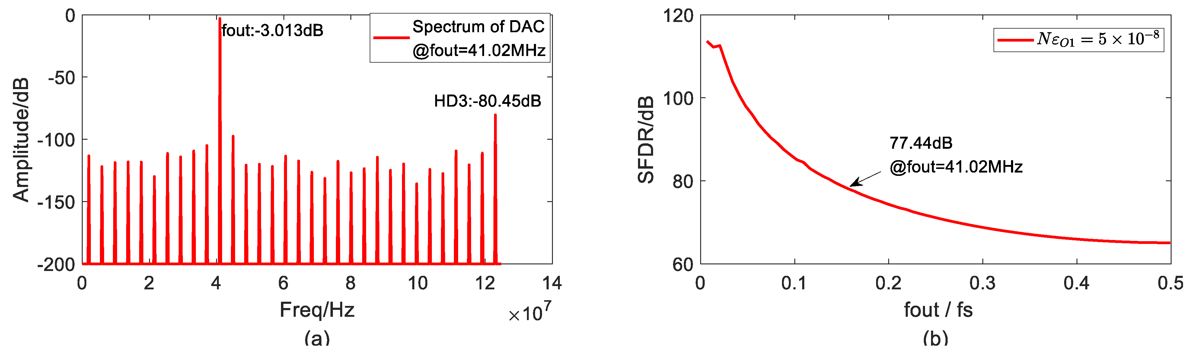
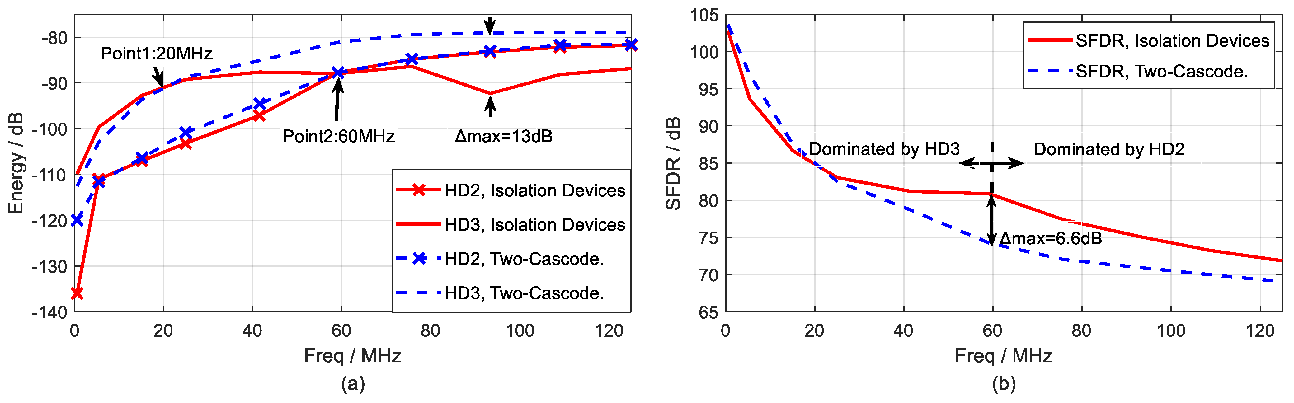
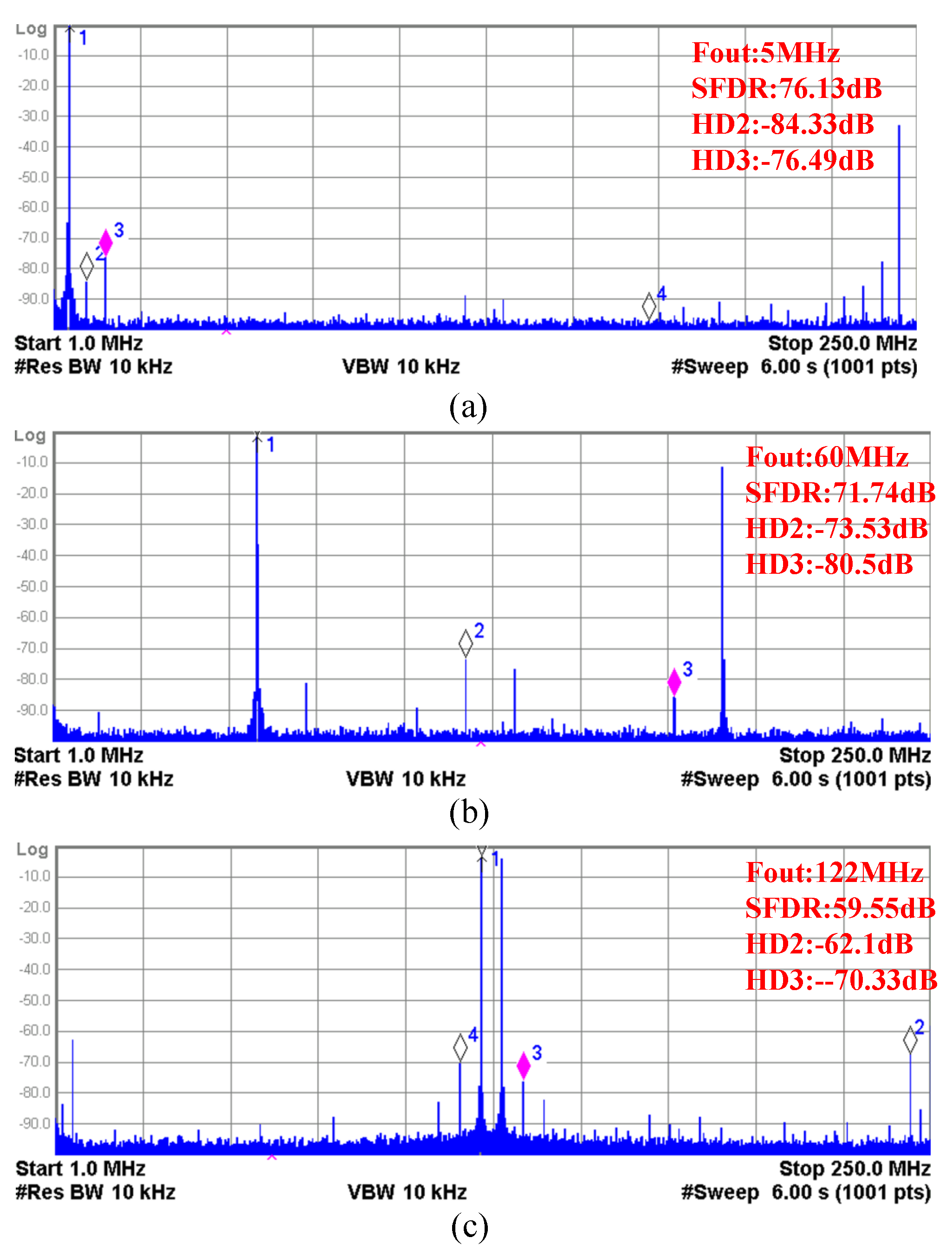
4. Measurement Results

Figure 12 illustrates the die micrograph and the layout of the proposed DAC. The area occupied by a single DAC is 3.06 mm × 2.14 mm. In this design, the current source array adopts a common centroid layout, and a large number of dummy devices are added to ensure the symmetry of the layout. Additionally, the AUX DAC can be programmed to either source or sink current, enabling it to effectively eliminate the DC offset of this DAC.
Figure 13 displays the measured curves of the DAC’s DNL and INL when the proposed calibration method was off. The DNL and INL are ±3LSB and ±13LSB, respectively. when the proposed calibration method was on, the DNL and INL of the DAC are within the ranges of ±2LSB and ±4LSB, as illustrated in Figure 14. Evidently, this calibration scheme significantly improves the linearity of the DAC.
Figure 15 shows the test spectrum of DAC at 5 MHz, 60 MHz, and 122 MHz, respectively. At 5 MHz, HD3 is approximately 8dB higher than HD2; meanwhile, at 60 MHz and the Nyquist frequency, HD3 is 7–8 dB lower than HD2. Comparing the spectra within the first Nyquist zone, at low-frequency outputs, HD3 is higher than HD2, determining the SFDR of the DAC. However, in the mid-to-high-frequency range, the new structure suppresses output-dependent errors, resulting in HD3 being lower than HD2 and thus no longer dominating the SFDR.
As depicted in Figure 16a, at an output frequency of 60MHz, the primary harmonic that dominates the DAC’s SFDR transitions from HD3 to HD2. Furthermore, when the output frequency exceeds 60 MHz, HD3 averages approximately 6 dB lower than HD2, suggesting that the isolation device effectively suppresses the influence of odd harmonics. When considering the third harmonic component alone, a significant suppression of the third harmonic can be observed in the mid-frequency range. This finding is consistent with the trends observed in simulation results and corroborates our previous analysis. In Figure 16b, the solid line represents the test results for the SFDR, and the dashed line depicts the attenuation curve due to the limited output impedance of the DAC as the frequency increases. It can be observed that the SFDR is elevated in the mid-to-high frequency range, indicating that the combination of the DQS structure and isolation components enhances the dynamic performance of the DAC in this frequency range.
Nevertheless, in this study, while the suppression of odd harmonics remains unaffected, the amplitude of HD2 is unexpectedly high in both simulation and measurement. The key factor contributing to this issue is the DQS structure, which comprises four switches that demand a high level of synchronization in their control signals. As discussed in work [23], the asymmetry among the switches can trigger the emergence of even harmonics.
A comparison of the performance of the proposed DAC with that of the state-of-the-art designs is presented in Table 1. Dummy circuits are added to each DQS switch to ensure the synchronization of the switches. These dummy circuits make the driving signal’s load the same, resulting in an increase in the area consumption of the entire DAC. Furthermore, the employment of calibration circuits and isolation devices necessitates a certain degree of area consumption. In this design, the low-frequency SFDR of the DAC is lower than that of work [19] and higher than that of work [15]. This is due to a slight decrease in the output impedance of the unit current source after adopting isolation devices. At the Nyquist frequency, the SFDR is superior to work [9] and is close to work [20,24].
Comparing with work [10], the scheme presented in this paper is not dependent on segmentation, making it significantly easier to design. The work [19] applies the same calibration scheme as this work, utilizing thermometer DEM to tackle voltage and time errors, thus achieving a better INL.
None of the other works incorporate calibration schemes and consequently fail to present the DNL and INL performance of the DAC. This ultimately accounts for the relatively smaller product area.

5. Conclusions

This work has analyzed the mechanism of output-dependent modulation in DACs based on a DQS structure. A comprehensive mathematical model has been developed, which theoretically explains the impact of originally ambiguous output-dependent errors on CS-DACs. Based on this model, a 16-bit 250 MS/s current-steering DAC is proposed.
A calibration scheme for improving the static performance of DAC has been proposed, enabling the DAC to achieve linearity with a DNL and INL of ±2LSB and ±4LSB, respectively.
Additionally, a novel switched current source structure is introduced, which integrates the DQS structure with always-on switches. The simulation results show that this structure suppresses odd harmonics caused by output-dependent errors by up to 13 dB, making the second-order harmonic dominant when calculating the spurious-free dynamic range (SFDR), resulting in a maximum improvement of the SFDR of 6.6dB, thereby significantly improving the dynamic performance of the DAC. The measurement results show that the SFDR of the DAC at the low-frequency output is 76.13 dB, 71.74 dB at 60 MHz, and 59.55 dB at 122 MHz after adopting the novel structure. The third harmonic is significantly suppressed in the mid-to-high frequency range, exhibiting the same trend to the simulation results, which is also in agreement with the proposed model.

Author Contributions

Conceptualization, Y.S. (Yingchao Sun); Methodology, Y.S. (Yingchao Sun); validation, Y.S. (Yingchao Sun) and Z.Z.; writing—original draft, Y.S. (Yingchao Sun); formal analysis, L.L. and Z.Z.; writing—review and editing, Z.Z., Y.D. and L.L.; supervision, Y.S. (Yi Shan) and Y.D.; project administration, Y.S. (Yi Shan) and Y.D.; funding acquisition, Y.S. (Yi Shan), L.L. and Y.D. All authors have read and agreed to the published version of the manuscript.

Funding

This work is supported by the Research Foundation of Strategic Priority Research Program of the Chinese Academy of Sciences (XDA18030100) and by the Shanghai Sailing Program (22YF1456400).

Data Availability Statement

Data are contained within the article.

Conflicts of Interest

The authors declare no conflicts of interest.

Appendix A

The derivation of the formula for distortion resulting from OSEs is presented as follows:
During each conversion, V 1 and V 2 represent the initial and final values of the DAC output, respectively. The output transition can be expressed as:
Δ V = V 2 V 1
Substituting Equations (A1) into (3) and (4), the OSEs can be reformulated as:
δ 01 = δ 11 = ε O 1 · V 2 V 1 + f Δ V 2
δ 10 = δ 00 = ε O 1 · V 2 V 1 f Δ V 2
Substituting Equations (A2) and (A3) into (5) and (6), the distortion introduced by OSEs can be reformulated as:
E r r O S , D Q S = E r r O S 1 = E r r O S 2 = V 2 N 2 · f Δ V + ε O 1 · N V 2 V 1
Considering the differences in switch transitions between DQS and normal structures, DACs with normal structures only includes two switching directions, δ 01 and δ 10 . Therefore, the distortion caused by the OSEs can be expressed as:
E r r O S 1 , N O R = Δ V δ 01 , i f V 1 < V 2
E r r O S 2 , N O R = Δ V δ 10 , i f V 1 > V 2
Substituting Equations (A2) and (A3) into (A5) and (A6), the distortion introduced by OSEs can be reformulated as:
E r r O S , N O R = q · V 2 V 1 2 ε O 1 + V 2 V 1 · f Δ V 2
where q can be expressed as:
q = 1 , i f V 2 > V 1 1 , i f V 2 < V 1
Represent q using V 1 and V 2 :
q = V 2 V 1 V 2 V 1
where V 1 = N 2 s i n w t + N 2 , V 2 = N 2 s i n w t + T s + N 2 .
To perform a trigonometric expansion on q:
q = n = 1 4 ( 2 n 1 ) π s i n [ ( 2 n 1 ) ( ω t + φ ) ]
where φ = a r c t a n s i n ω T S c o s ω T S 1 .
In Equation (A7), ( V 2 V 1 ) 2 can be described as:
V 2 V 1 2 = N 2 s i n 2 ω T S 2 s i n 2 ω t + φ
By utilizing Formulas (A10) and (A11), the SFDR performance degradation caused by the OSEs can be easily calculated and plotted. Similarly, the error analysis for SSEs and BEEs is also conducted in the same manner.

References

  1. van den Bosch, A.; Steyaert, M.; Sansen, W. SFDR-bandwidth limitations for high speed high resolution current steering CMOS D/A converters. In Proceedings of the ICECS’99—Proceedings of ICECS ’99. 6th IEEE International Conference on Electronics, Circuits and Systems (Cat. No.99EX357), Paphos, Cyprus, 5–8 September 1999; Volume 3, pp. 1193–1196. [Google Scholar] [CrossRef]
  2. Luschas, S.; Lee, H.S. Output impedance requirements for DACs. In Proceedings of the 2003 International Symposium on Circuits and Systems, Bangkok, Thailand, 25–28 May 2003; Volume 1. [Google Scholar] [CrossRef]
  3. Chen, T.; Gielen, G. Modelling of the impact of the current source output impedance on the SFDR of current-steering CMOS D/A converters. In Proceedings of the 2004 IEEE International Symposium on Circuits and Systems (ISCAS), Vancouver, BC, Canada, 23–26 May 2004; Volume 1. [Google Scholar] [CrossRef]
  4. Galton, I. Why Dynamic-Element-Matching DACs Work. IEee Trans. Circuits Syst. II Express Briefs 2010, 57, 69–74. [Google Scholar] [CrossRef]
  5. Lee, D.H.; Kuo, T.H.; Wen, K.L. Low-Cost 14-Bit Current-Steering DAC With a Randomized Thermometer-Coding Method. IEEE Trans. Circuits Syst. II Express Briefs 2009, 56, 137–141. [Google Scholar] [CrossRef]
  6. Tong, X.; Liu, D. High SFDR Current-Steering DAC with Splitting-and-Binary Segmented Architecture and Dynamic-Element-Matching Technique. IEEE Trans. Circuits Syst. II Express Briefs 2022, 69, 4233–4237. [Google Scholar] [CrossRef]
  7. Park, S.; Kim, G.; Park, S.C.; Kim, W. A digital-to-analog converter based on differential-quad switching. IEEE J. Solid-State Circuits 2002, 37, 1335–1338. [Google Scholar] [CrossRef]
  8. Schafferer, B.; Adams, R. A 3 V CMOS 400 mW 14b 1.4GS/s DAC for multi-carrier applications. In Proceedings of the 2004 IEEE International Solid-State Circuits Conference (IEEE Cat. No.04CH37519), San Francisco, CA, USA, 15–19 February 2004; Volume 1, pp. 360–532. [Google Scholar] [CrossRef]
  9. Engel, G.; Kuo, S.; Rose, S. A 14b 3/6GHz current-steering RF DAC in 0.18 μm CMOS with 66 dB ACLR at 2.9 GHz. In Proceedings of the 2012 IEEE International Solid-State Circuits Conference, San Francisco, CA, USA, 19–23 February 2012; pp. 458–460. [Google Scholar] [CrossRef]
  10. Liu, M.; Zhu, Z.; Yang, Y. A High-SFDR 14-bit 500 MS/s Current-Steering D/A Converter in 0.18 μm CMOS. IEEE Trans. Very Large Scale Integr. (VLSI) Syst. 2015, 23, 3148–3152. [Google Scholar] [CrossRef]
  11. Wang, F.; Wang, Z.; Liu, J.; Yu, F. A 14-Bit 3-GS/s DAC Achieving SFDR >63dB Up to 1.4 GHz With Random Differential-Quad Switching Technique. IEEE Trans. Circuits Syst. II Express Briefs 2022, 69, 879–883. [Google Scholar] [CrossRef]
  12. Lai, L.; Li, X.; Fu, Y.; Liu, Y.; Yang, H. Demystifying and Mitigating Code-Dependent Switching Distortions in Current-Steering DACs. IEEE Trans. Circuits Syst. I Regul. Pap. 2019, 66, 68–81. [Google Scholar] [CrossRef]
  13. Tseng, W.H.; Lin, W.; Hsu, C.W.; Huang, C.Y.; Lin, Y.S.; Huang, H.Y.; Chen, H.; Liao, S.H.; Chen, K.D.; Strange, J.; et al. 17.3 A 14b 16 GS/s Time-Interleaving Oirect-RF Synthesis OAe with T-OEM Achieving −70dBc IM3 up to 7.8 GHz in 7 nm. In Proceedings of the 2023 IEEE International Solid-State Circuits Conference (ISSCC), San Francisco, CA, USA, 19–23 February 2023; pp. 268–270. [Google Scholar] [CrossRef]
  14. Kong, D.; Rivas-Rivera, K.; Galton, I. A 600-MS/s DAC with over 87-dB SFDR and 77-dB Peak SNDR Enabled by Adaptive Cancellation of Static and Dynamic Mismatch Error. IEEE J. Solid-State Circuits 2019, 54, 2219–2229. [Google Scholar] [CrossRef]
  15. Huang, H.Y.; Chen, X.Y.; Kuo, T.H. A 10-GS/s NRZ/Mixing DAC With Switching-Glitch Compensation Achieving SFDR >64/50 dBc over the First/Second Nyquist Zone. IEEE J. Solid-State Circuits 2021, 56, 3145–3156. [Google Scholar] [CrossRef]
  16. Huang, H.Y.; Chen, X.Y.; Kuo, T.H. A 177 mW 10GS/s NRZ DAC with Switching-Glitch Compensation Achieving > 64 dBc SFDR and <−77 dBc IM3. In Proceedings of the 2020 IEEE Symposium on VLSI Circuits, Honolulu, HI, USA, 16–19 June 2020; pp. 1–2. [Google Scholar] [CrossRef]
  17. Huang, H.Y.; Kuo, T.H. A 0.07-mm2 162-mW DAC Achieving >65 dBc SFDR and < −70 dBc IM3 at 10 GS/s with Output Impedance Compensation and Concentric Parallelogram Routing. IEEE J. Solid-State Circuits 2020, 55, 2478–2488. [Google Scholar] [CrossRef]
  18. Lin, C.H.; van der Goes, F.; Westra, J.; Mulder, J.; Lin, Y.; Arslan, E.; Ayranci, E.; Liu, X.; Bult, K. A 12b 2.9GS/s DAC with IM3 ≪-60dBc beyond 1GHz in 65nm CMOS. In Proceedings of the 2009 IEEE International Solid-State Circuits Conference—Digest of Technical Papers, San Francisco, CA, USA, 8–12 February 2009; pp. 74–75, 75a. [Google Scholar] [CrossRef]
  19. Lin, C.H.; Wong, K.L.J.; Kim, T.Y.; Xie, G.R.; Major, D.; Unruh, G.; Dommaraju, S.R.; Eberhart, H.; Venes, A. A 16b 6GS/S nyquist DAC with IMD <−90 dBc up to 1.9 GHz in 16nm CMOS. In Proceedings of the 2018 IEEE International Solid-State Circuits Conference—(ISSCC), San Francisco, CA, USA, 11–15 February 2018; pp. 360–362. [Google Scholar] [CrossRef]
  20. Van de Vel, H.; Briaire, J.; Bastiaansen, C.; van Beek, P.; Geelen, G.; Gunnink, H.; Jin, Y.; Kaba, M.; Luo, K.; Paulus, E.; et al. 11.7 A 240 mW 16b 3.2 GS/s DAC in 65 nm CMOS with <−80 dBc IM3 up to 600 MHz. In Proceedings of the 2014 IEEE International Solid-State Circuits Conference Digest of Technical Papers (ISSCC), San Francisco, CA, USA, 9–13 February 2014; pp. 206–207. [Google Scholar] [CrossRef]
  21. Mercer, D.A. Low-Power Approaches to High-Speed Current-Steering Digital-to-Analog Converters in 0.18-μm CMOS. IEEE J. Solid-State Circuits 2007, 42, 1688–1698. [Google Scholar] [CrossRef]
  22. Dongmei, Z.; Dongbing, F.; Jiangang, S.; Kaicheng, L. Digital static calibration technology used for 400MSPS, 16-bit DAC. In Proceedings of the 2009 IEEE International Conference of Electron Devices and Solid-State Circuits (EDSSC), Xi’an, China, 25–27 December 2009; pp. 91–94. [Google Scholar] [CrossRef]
  23. Andersson, K.; Vesterbacka, M. Modeling of glitches due to rise/fall asymmetry in current-steering digital-to-analog converters. IEEE Trans. Circuits Syst. I Regul. Pap. 2005, 52, 2265–2275. [Google Scholar] [CrossRef]
  24. Su, S.; Chen, M.S.W. A 16b 12GS/S single/dual-rate DAC with successive bandpass delta-sigma modulator achieving <−67 dBc IM3 within DC-to-6 GHz tunable passbands. In Proceedings of the 2018 IEEE International Solid-State Circuits Conference—(ISSCC), San Francisco, CA, USA, 11–15 February 2018; pp. 362–364. [Google Scholar] [CrossRef]
Figure 1. The (a) circuit and (b) timing sequence of the DQS structure.
Electronics 13 01992 g001
Figure 2. (a) Simulation configuration and (b) results of the OSEs.
Electronics 13 01992 g002
Figure 3. (a) Simulation configuration and (b) results of the SSEs.
Electronics 13 01992 g003
Figure 4. The impact of output transition on SFDR with different output frequencies: (a) spectrum and (b) SFDR.
Electronics 13 01992 g004
Figure 5. (a) Simulation configuration and (b) results of the BEEs.
Electronics 13 01992 g005
Figure 6. Simulation results of the impact of ODM on SFDR in (a) normal and (b) DQS structures.
Electronics 13 01992 g006
Figure 7. Block diagram of the overall model.
Electronics 13 01992 g007
Figure 8. Structure of the proposed DAC.
Electronics 13 01992 g008
Figure 9. (a) Calibration scheme and (b) circuit of calibration of the DAC.
Electronics 13 01992 g009
Figure 10. Suppressing effects of isolation devices on (a) SSEs and (b) BEEs.
Electronics 13 01992 g010
Figure 11. The simulation results of (a) harmonics and (b) SFDR of DACs adopting the two structures separately.
Electronics 13 01992 g011
Figure 12. Die micrograph and layout of the proposed DAC.
Electronics 13 01992 g012
Figure 13. Measured (a) DNL and (b) INL when the proposed calibration method was off.
Electronics 13 01992 g013
Figure 14. Measured (a) DNL and (b) INL when the proposed calibration method was on.
Electronics 13 01992 g014
Figure 15. The test spectrum of the DAC at (a) Fout = 5 MHz; (b) Fout = 60 MHz; (c) Fout = 110 MHz.
Electronics 13 01992 g015
Figure 16. The test results of (a) harmonics and (b) SFDR of the proposed DAC.
Electronics 13 01992 g016
Table 1. Comparison with precious studies.
This WorkISSCC [9]ISSCC [20]VLSI [10]JSSC [15]ISSCC [19]ISSCC [24]
Resolution (bit)16141614141616
Process (nm)18018065180281665
Supply (V)1.8/3.31.8/31.2/3.33.31.11.0/3.3-
F c l k (MS/s)2502900320050010,000600012,000
Area (mm2)6.554-0.550.10.525
DNL/INL(LSB)±2/±4-----/±0.25-
S F D R b e s t (dB)76.13848483.774.38876
S F D R n y q (dB)59.55525868.964.56759
F o m [6] (GHz/mW)
2 N · F S / P t o t a l 95.4136.5873.8121925.61123446.8
Disclaimer/Publisher’s Note: The statements, opinions and data contained in all publications are solely those of the individual author(s) and contributor(s) and not of MDPI and/or the editor(s). MDPI and/or the editor(s) disclaim responsibility for any injury to people or property resulting from any ideas, methods, instructions or products referred to in the content.

