
Implementing Demons and Ratchets

ThermaWatts, LLC, Renton, WA 98057, USA
*
Author to whom correspondence should be addressed.
Entropy 2017, 19(1), 34; https://doi.org/10.3390/e19010034
Submission received: 30 November 2016
/
Revised: 5 January 2017
/
Accepted: 6 January 2017
/
Published: 14 January 2017
(This article belongs to the Special Issue Limits to the Second Law of Thermodynamics: Experiment and Theory)
Abstract
:Experimental results show that ratchets may be implemented in semiconductor and chemical systems, bypassing the second law and opening up huge gains in energy production. This paper summarizes or describes experiments and results on systems that effect demons and ratchets operating in chemical or electrical domains. One creates temperature differences that can be harvested by a heat engine. A second produces light with only heat input. A third produces harvestable electrical potential directly. These systems share creating particles in one location, destroying them in another and moving them between locations by diffusion (Brownian motion). All absorb ambient heat as they produce other energy forms. None requires an external hot and cold side. The economic and social impacts of these conversions of ambient heat to work are, of course, well-understood and huge. The experimental results beg for serious work on the chance that they are valid.
1. Introduction
This paper is intended to assist understanding possible second law exceptions, so that readers might be moved to examine them carefully.
The second law of thermodynamics was first expressed more than 190 years ago to show that there is an upper limit to the efficiency of a heat engine, which converts heat to mechanical energy or other work. Simply put, such conversion always suffers inefficiency. The second law has been thoroughly tested, restated and confirmed many times since then [1].
Scientists have shifted away from the notion of “laws” to ideas about “models” to explain and predict behaviors, because laws imply completeness, whereas models acknowledge their incompleteness. This gives freedom to expand our range of thinking, including that on the second law. A small set of researchers has made the transition to models as they develop experiments that point to new energy possibilities. They seem to be driven by the potentially huge value to humanity for finding such possibilities [2].
We present below three cases of systems that may be demonstrating demons and ratchets. These were chosen because:
- They are supported by test results;
- We believe they are conceptually clean and easily explained; and
- They may have commercial application.
We believe that if any one of these demonstrations is valid (we believe all are), it opens up a range of practical methods for turning ambient heat directly into electrical energy. This matters because such direct conversion can be perfectly sustainable, since it does not require fuels or otherwise cause environmental damage.
The cases are:
- Epicatalysis: Tests demonstrate that opposing catalysts can create a temperature differential needed for a heat engine heat.
- LEDs: Emission measurements show that unbiased light emitting diodes (LED’s) emit a small amount of light.
- Doped semiconductor structure: A sandwich-like structure of semiconductors presents a persistent, harvestable voltage. We call this an ambient thermal electric converter (ATEC).
The demonstration systems have two features in common: particles are created and destroyed, and these actions take place at different locations.
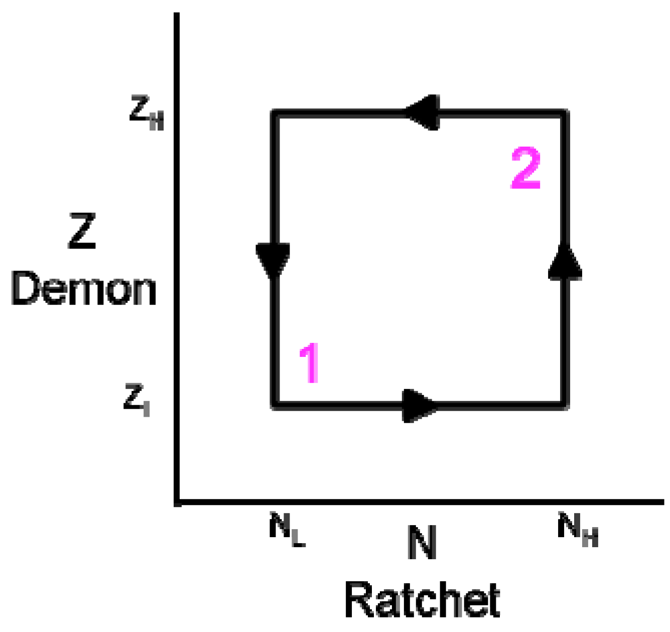
Figure 1 shows the general concept for a cycle that would create an exception to the second law. Z represents some potential or work function. It could be gravity, electric potential or some other function. N represents the number of particles in the system.
The flow is as follows:
- The bottom line represents the creation of particles at Location 1.
- Some particles move across the potential to Location 2, driven by thermal energy through diffusion. This creation process fills the role of Maxwell’s demon.
- Some of those particles are then destroyed.
- Remaining particles return to Location 1.
The changing number of particles fills the role of a Brownian ratchet. There is much flexibility in implementing this cycle, as described below. The directional bias is essential.
The overall cycle converts thermal energy into some other form of energy and then prevents the reverse transition by removing the particles involved. Cheating the laws of physics once is not enough; we have to do it twice: both Maxwell’s demon and a Brownian ratchet are required.
The general concept that captures the objection to the cycle of Figure 1 is “detailed balance”. The principle of detailed balance says that both paths between 1 and 2 should be in equilibrium. In that regard, the principle of detailed balance is the most narrowly focused reason why such cycles should not work. In other words, the principle of detailed balance is a corollary to the second law.
Note: this paper only summarizes the methods and results of epicatalysis, part of the LED emissions experiments and the doped semiconductor structure (ATEC) to permit the reader to see the similarities of the systems without getting lost in the details. Thus, the reader is encouraged to examine the Supplemental Materials and references for further depth of understanding.
2. Materials and Methods
The subsections below describe the setup and processes we used to test the hypotheses that certain systems convert heat to work without a cold side. We intend that the information in this section and our “A Report on Testing of ThermaWatts Prototype Ambient Thermal Electric Converter Devices” document, accessible through the Supplementary Materials, are sufficient for replication of our work by others.
2.1. LEDs
Two methods are described that we used to capture the effect of unbiased LEDs emitting light.
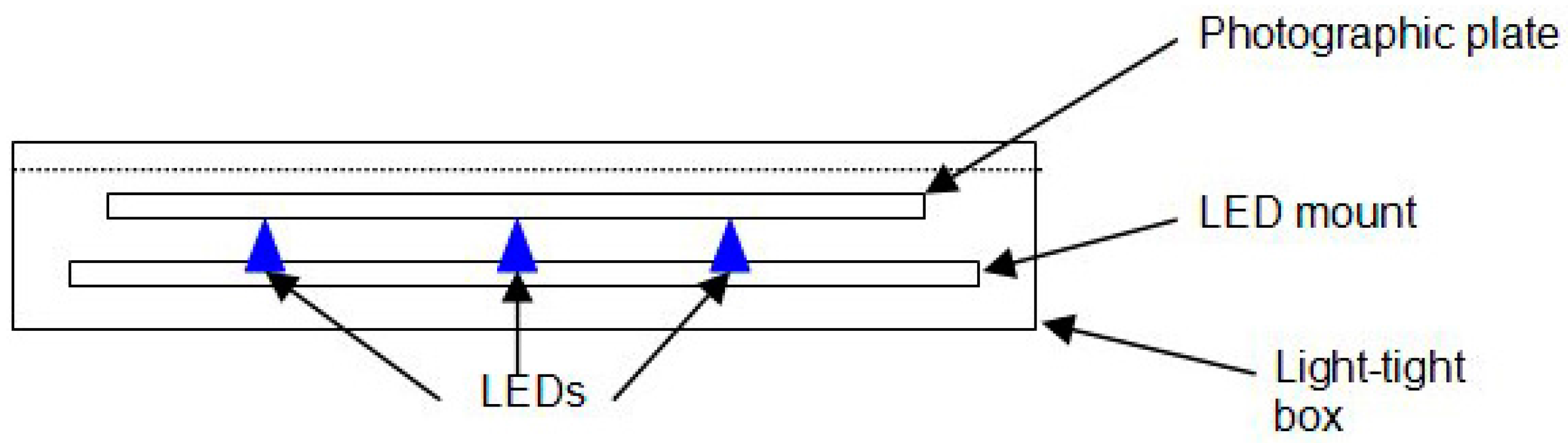
2.1.1. Direct Film Exposure
In 2007–2008, Peter Orem set up a simple apparatus to try to record photons that might be emitted from an unbiased LED upon photo-recombination of electrons and holes.
The apparatus is as shown in Figure 2. Several LEDs of various types were mounted on a printed circuit board, each with its contact leads shorted together. High speed (Fuji Superia 3200, Tokyo, Japan) color film was mounted in parallel to the board with LEDs. Working in a dark room, that assembly was put together in a light-tight plastic box (Hammond 1594EBK, Guelph, ON, Canada), which in turn was sealed with black tape. The assembly sat on a shelf for several months, after which the film was extracted (again in a dark room). The film was then taken to a commercial service for development.
Sample exposures are shown in Section 3.
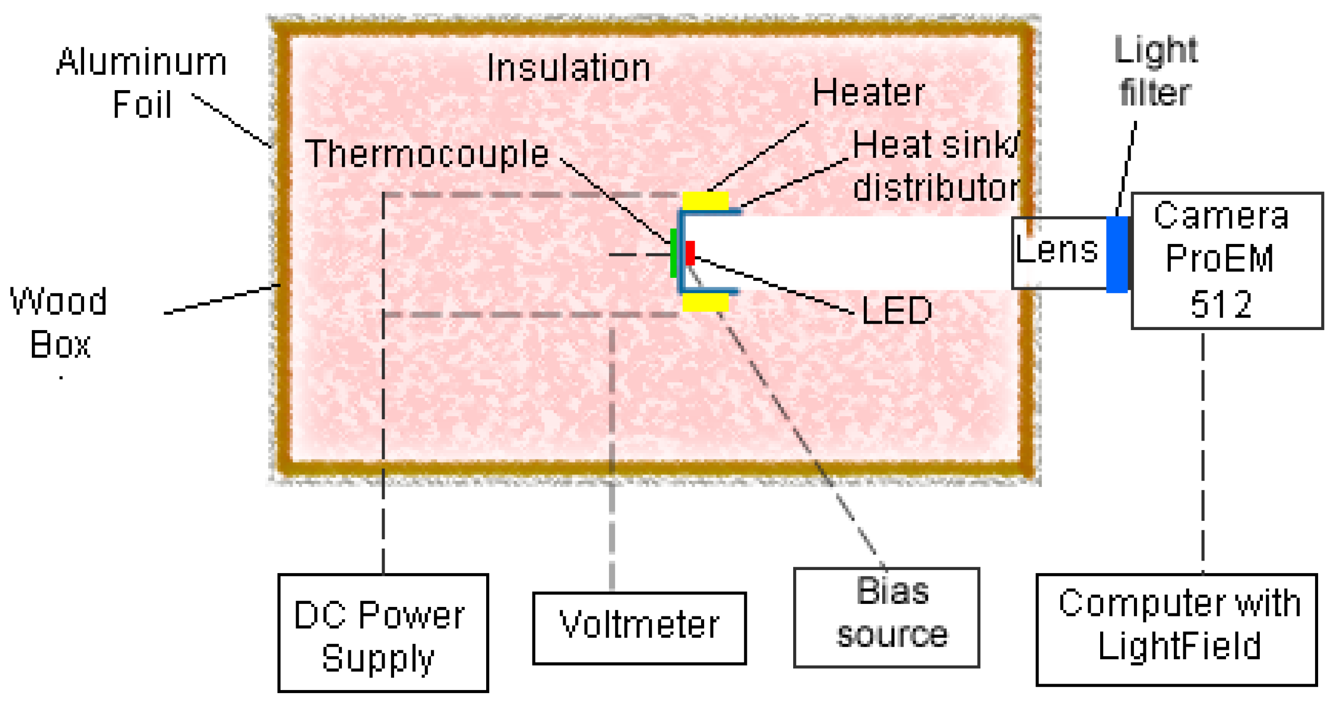
2.1.2. Digital Imaging of Heated, Unbiased LED
Like the direct film exposure above, the apparatus was devised to capture photons that might be emitted from an unbiased LED upon recombination of electrons and holes. The apparatus is shown in Figure 3.
The camera is a ProEM 512® from Princeton Instruments (Trenton, NJ, USA). It uses their lowest pixel resolution to minimize the exposure time needed for each pixel. It has a relatively high quantum efficiency to capture near infrared from the LED. A light filter is mounted in the lens. A computer with Princeton Instrument’s LightSource® software Version 6.0 drives camera operation and captures image output. The LED is held against a heat sink/distributor (for good heat transfer) by a spring clip. Twisted conductors are run from the LED leads to a switchable bias source (open, shorted, +1.5 V, 1.5 V). The heat sink/distributor has heating resistors attached (2 × 20 Ω in parallel, 50 W), which are in turn driven at up to 90 watts from a variable DC power supply. Temperature at the heat sink/distributor is measured by a thermocouple. The heat sink/distributor, heater and LED assembly is housed in a fiberglass-filled wood box and covered with aluminum foil. The camera and box are mounted firmly together to maintain focal distance to the LED. Tests are run in a dark room.
The light filter and target LED are selected to have matching wavelengths at 940 nm. The light filter is a ThorLabs bandpass filter, CWL = 940, FWHM = 10 (centered at 940 nm, with a width of ±10 nm). The LED is a Fairchild semiconductor QEB363ZR—LED IR EMITTING 940 NM 2MM ZB T/R (Digikey QEB363ZRCT-ND, Phoenix, AZ, USA).
The tests may be run with the heat sink/distributor held at a temperature (per thermocouple/voltmeter) in steady state at up to 196 °C. Exposure times are typically up to an hour long per frame.
Sample exposures are shown in the Results.
2.2. Doped Semiconductor Structures (ATEC)
An ATEC is a semiconductor sandwich of high and low density semiconductors, with alternate n-doped and p-doped layers between, as described in Section 4.2.
2.2.1. The ATEC Structure
Several prototype ATECs were built at Stanford University per the specifications listed in the Supplemental Materials, Test Results, Section 2: Conceptual Design.
Figure 4 shows one of the ATEC prototypes we had fabricated.
- It is 10 ½ cycles of AlGaAs with either 33% or 50% Al, 5.5 µm thick
- It is on a base of n-GaAs, 0.5 mm thick and 75 mm (3”) in diameter
- It has a gold conductor final layer. The surface features you see are reflections of the room.
2.2.2. Simulation Tools
Modeling used Silvaco’s Atlas 5.16.3.R, which includes simulation software and semiconductor materials’ data.
2.2.3. Laboratory Test Tools
The custom test jig and tools were developed to address the considerable challenges of testing (see the Supplemental Materials, Test Results, and Section 3: Model Results). Primary challenges are listed below.
- Costs: since our prototype ATEC material set was constrained by costs, we could look for only microvolt outputs, which are hard to measure without high-end equipment (also cost-constrained)
- Seebeck effect
- Voltage across the ATEC from electrical noise induced through wiring and the ATEC and then rectified by the ATEC, which is inherently a diode
- Meter bias
We are looking for any output voltage across the ATEC at zero input.
To establish confidence and credibility for our test method, we collected data points either side of zero input: a sweep. The sweep order was programmed to run from a small positive voltage to maximum positive voltage and from small negative voltage down to maximum negative voltage. There was a 40-s delay from sweep voltage setting to voltage measurement mitigating the effects of system capacitance. The zero sweep voltage point output should fall on the straight line of outputs from the rest of the sweep. Interim data were recorded and inspected for stability. All sweep data are available at the ThermaWatts, LLC website [3].
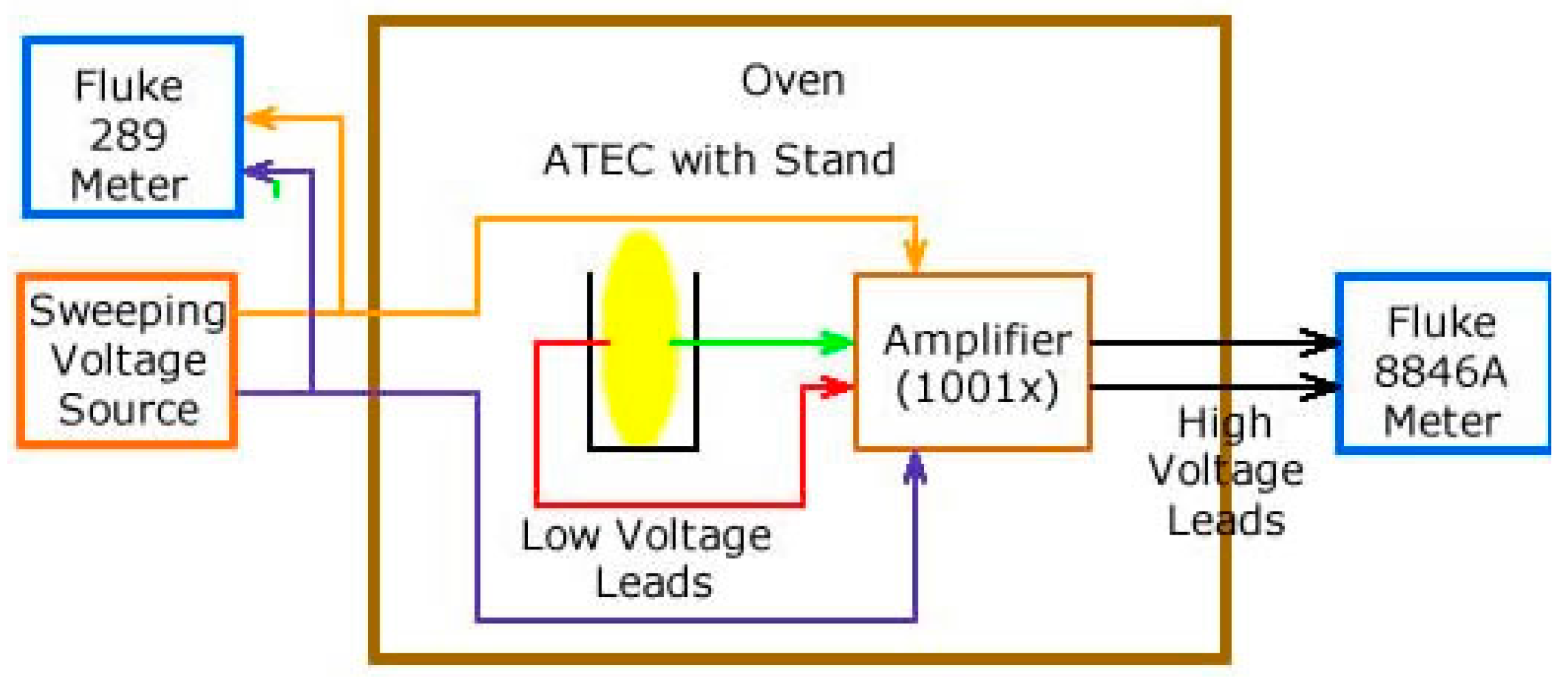
Figure 5 is the top-level view of the test apparatus. It shows the source of sweep voltage and the measurement of net voltage (sweep voltage plus any contribution by the ATEC) across the ATEC.
Our approach to tackle the several challenges was to:
- Apply a known sweep voltage to the ATEC and a known resistor in series
- Amplify the voltage across the known resistor to bring it from the microvolt to millivolt range
- Put the test target, measurement circuitry and wiring (as much as possible) into the oven (environmental chamber)
- Design all low voltage signals such that they are in a small region at a uniform temperature, with short wires; longer runs were amplified (or not yet divided) by 1000 or 4000, respectively.
Figure 6 shows a somewhat more detailed view of the test jig used to meet these challenges while finding the zero sweep voltage output of the ATEC.
The complete circuit for driving the sweep voltage and detecting net voltage is shown in Figure 7. It is described in the Supplemental Materials, Test Results, and Section 5: Test Setups and Procedures.
Figure 8 shows:
- ATEC on a stand, with wiring, inside an environmental chamber.
- ATEC on a custom ceramic stand, with contact wires.
- Relay control board and Arduino processor for sweep control logic.
3. Results
The results of the two experimental areas identified in the Materials and Methods are summarized here:
- Unbiased LEDs emitting light
- Harvestable voltage across a doped semiconductor structure (ATEC)
Additional data are available in the Supplemental Materials, Test Results, and Section 4: Test Results.
3.1. LEDs
Test results to determine if unbiased LEDs emit light consist of photographic images collected by different methods (direct film exposure and digital images).
3.1.1. Direct Film Exposure
In our first experiment on LED emissions, a strip of film was exposed to a set of LEDs (each with its leads tied together) for a period of several months (see Section 2.1.1 in the Materials and Methods). When developed, the film showed frames like the one in Figure 9 (which contains the clearest effect we were looking for, while containing no obvious flaws). The glowing areas, one small and focused, one large and blurred, are arguably the result of photons emitted from two LEDs.
3.1.2. Digital Imaging of Heated, Unbiased LED
Images from our second experiment for LED emissions, set up per 2.1.2 in the Materials and Methods, are shown and described below.
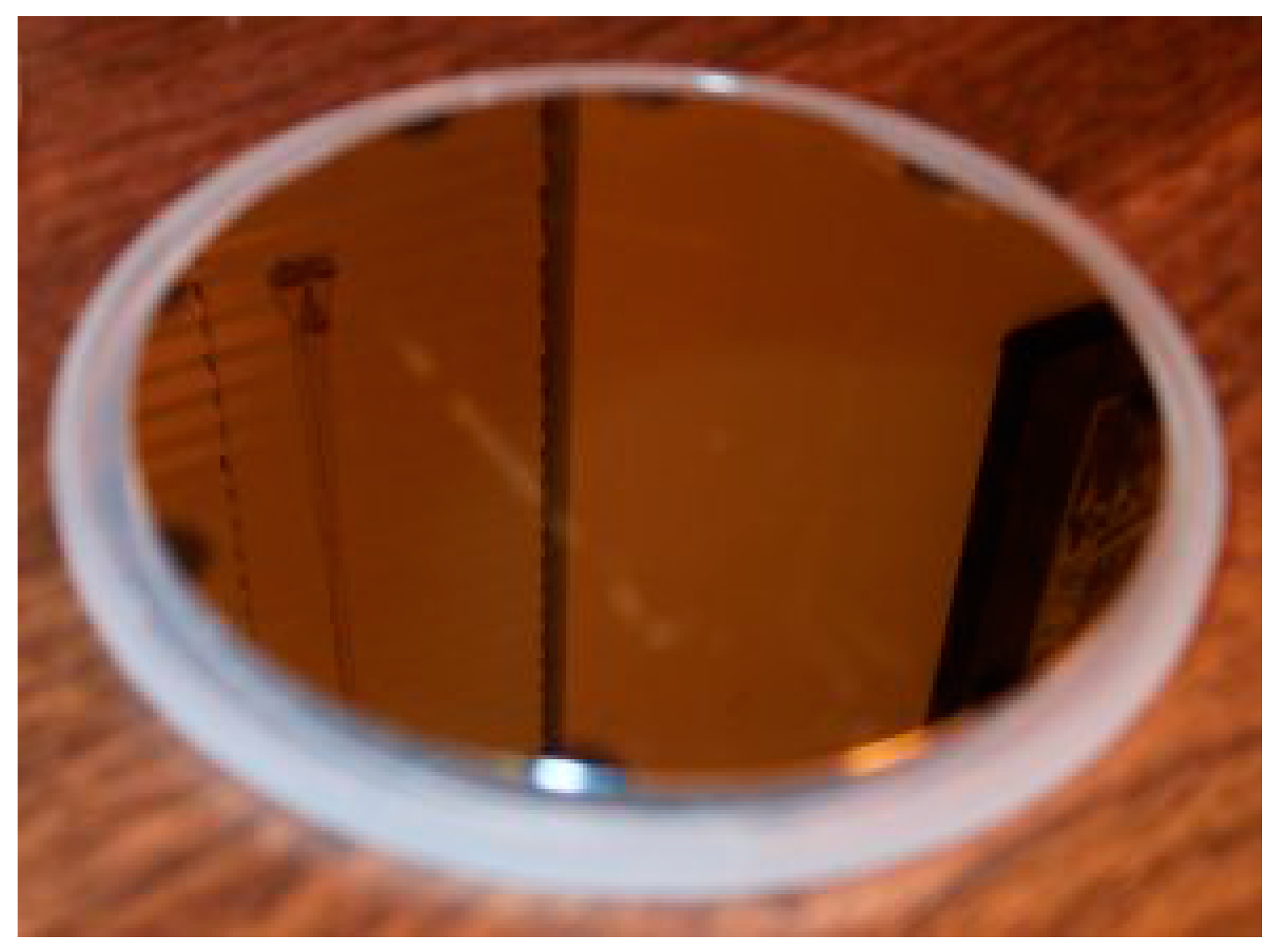
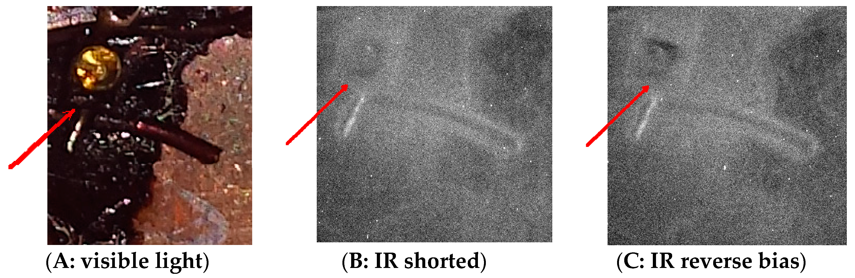
Figure 10 shows the camera view of a 940-nm LED mounted on the heat sink/distributor within the digital imaging box. Frame A was taken by a digital camera in room lighting. The LED is the golden circle, upper left. The black material is rosin from soldering. Frames B and C show the view as seen by the Princeton Instruments ProEM 512® camera through LightField® 6.0 software, with the heat sink/distributor warmed to 196 °C. The test room was dark. Exposure time for each was 30 min. The only known differences between the images in Frames B and C is the connection of the LED leads. For Frame B, the leads are open. For Frame C, the leads are connected to battery that applies a 1.5-V reverse bias.
The images in Frames B and C are distinctly different in the region of the LED (above the red arrow) and otherwise quite similar. In Frame C, there appears to be less light at the LED.
3.2. Doped Semiconductor Structure
Testing of our ATEC consisted of modeling the structure and then running extensive measurements against prototype ATECs.
3.2.1. Simulation
Before we had the prototype ATEC fabricated, we ran models on its structure and materials.
Figure 11 shows modeled behavior of AlGaAs in the configuration for an ATEC. The graph shows a non-zero flow of electrons and holes through the ATEC. Additional results are in the Supplemental Materials, Test Results, and Section 3: Model Results.
These results encouraged us to move to prototyping and laboratory tests.
3.2.2. Laboratory Tests
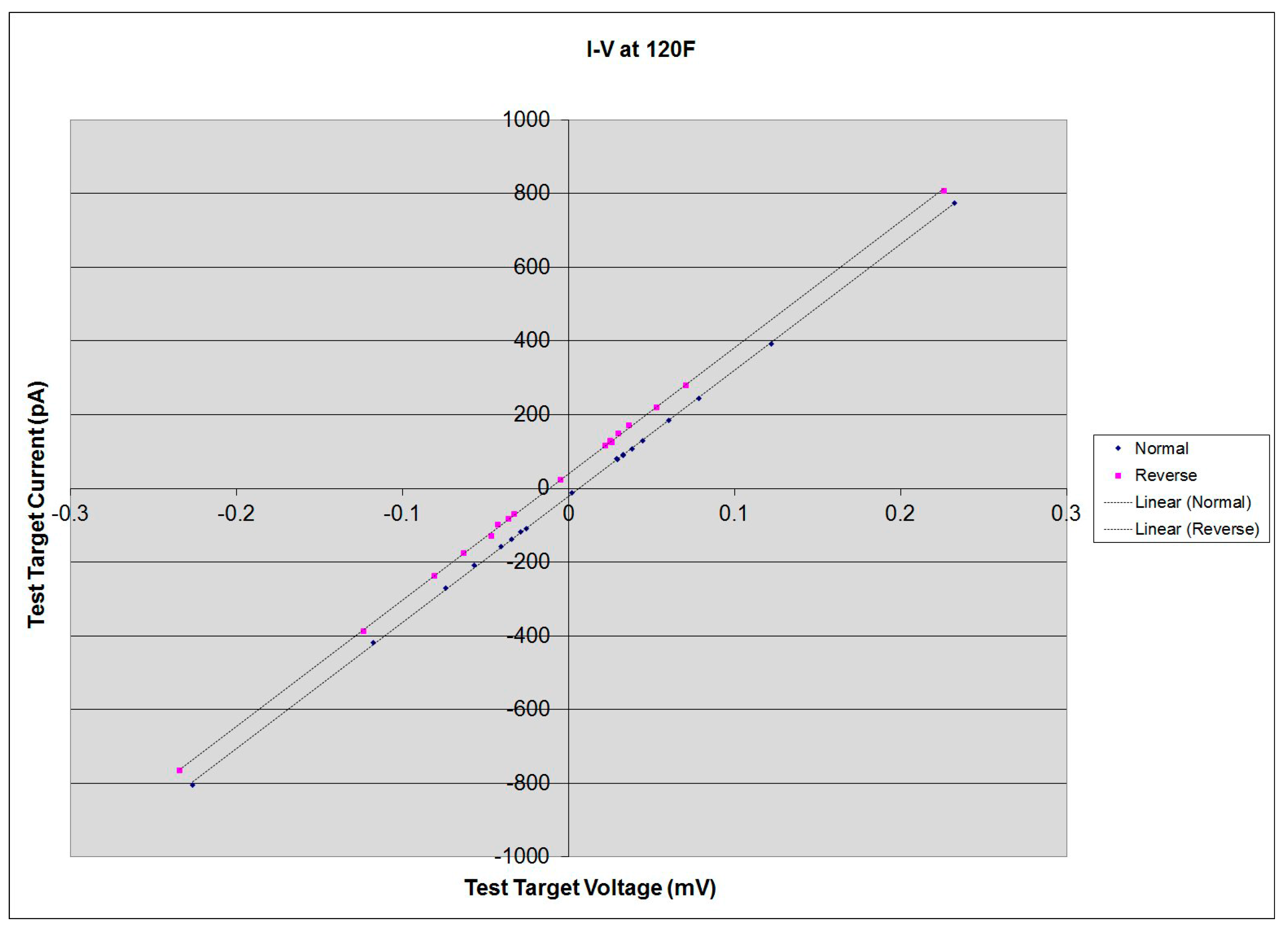
Prototype ATECs were tested, with considerable care given to holding sources of error to negligible levels. As an imposed voltage was swept across a prototype, the measured output voltage was consistently different from the imposed voltage (see the Supplemental Materials, Test Results, and Section 4: Test Results).
We held temperature steady, so there should be no Seebeck effect, applied a bias sweep, and measured current. At zero bias, we remove all power near the oven/cage so that there was very little opportunity for EMI to be rectified to enter the measurement.
The graph shows:
- Parallel lines across the sweep of bias, one for each orientation of the ATEC. The blue dots are from the “normal” ATEC orientation, and the red dots are for “reverse.”
- Linear offset of voltage across the target.
The plots for voltage across the ATEC do not pass through zero current at zero voltage. The offsets between those plots are opposite and about equal at zero bias.
This strongly suggests that the prototype contributed its own voltage (half the distance between the lines), either with or in opposition to the imposed voltage, depending on which way the prototype was turned.
We take the difference as twice the contribution to voltage made by the target ATEC
Figure 13 shows the results from runs made at 160 °F with an ATEC and then with resistors of 160 K Ohm and 220 K Ohm.
- The ATEC normal and reverse run results are again separated and again do not pass through zero current at zero voltage;
- The resistor plots both pass through zero (at this scale) and have different slopes, as expected.
We also ran tests for photosensitivity, flooding the target with AC noise and the effects of flexing the target (see the Supplemental Materials, Test Results, and Section 4: Test Results). The results were consistent with the models.
We conclude that the target ATEC is producing electricity and surmise that it is absorbing heat to satisfy the conservation of energy.
4. Discussion
This section describes systems under test that demonstrate conversion of ambient heat to useful work.
4.1. Epicatalysis
Catalysts have been used to assist in chemical reactions for about 200 years. They may speed up a reaction and lower energy requirements, but do not change the chemical equilibrium (completeness of a reaction). While they participate in reactions, they are not consumed.
The term “epicatalysis” is used to identify pairs of catalysts that oppose each other in assisting a chemical reaction, such that their chemical equilibrium points are different. The idea has been around for more than 100 years, with several supporting experiments.
If one puts two catalysts with opposing characteristics in contact with a bath of chemical reactants, per Figure 14, three things will occur:
- Catalyst 1 one will create Reactant Set A in favor of Reactant Set B, and Catalyst 2 will create Reactant Set B in favor of Reactant Set A.
- By diffusion, the bath will tend to equalize the reactants in the reverse direction, B diffusing toward Catalyst 1 and A toward Catalyst 2.
- One of the reactions (A => B or B => A) will generate more net heat (be exothermic) than the other, so the catalyst surface will warm, and the other will absorb more net heat (be endothermic).
The difference in net heat (and therefore temperature) may be used to drive a heat engine with no external cold side.
Since the reactants and the catalysts are not consumed, the process will continue indefinitely. If heat is added to the bath, the temperature difference at the catalysts may be harvested, perhaps as electricity using the Seebeck effect, indefinitely.
Dr. Daniel Sheehan [4,5,6] and David Miller [7] have experimental data on temperature differences created by epicatalysis. Such differences should support a heat engine operating only with ambient heat (no cold side).
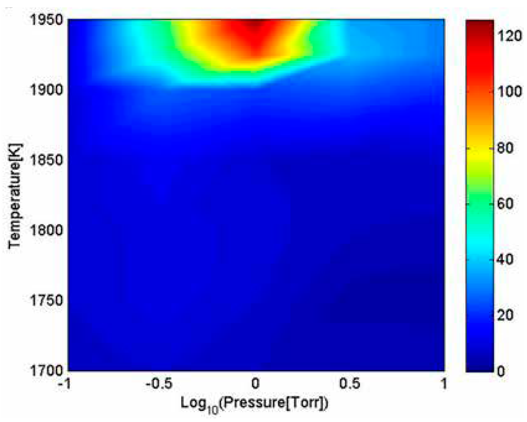
Sheehan used hydrogen as the bath and catalysts of rhenium (Re) and tungsten (W). The reactions were molecular hydrogen H2 to atomic hydrogen H at the rhenium catalyst and H to H2 at the tungsten catalyst, as shown in Figure 15. See [6] for complete interpretation of Figure 15.
Because these reactions only take place significantly at high temperatures, the bath and measurement apparatus were heated to 1950 °K. Sheehan measured the difference in temperature at the catalysts at up to 126 °K (see Figure 16, which shows the temperature difference between catalysts as temperature increases, and see [6] for complete interpretation of Figure 16). This temperature difference could be harvested as electricity indefinitely, with heat supplied as part of maintaining bath temperature.
David Miller [7] is working toward parallel results using formic acid and other low-strength hydrogen bond chemicals with catalyst surfaces, such as Teflon, and at typical environmental temperatures. He has achieved a temperature differential of about 0.2 °C. His work continues to explore combinations of materials and catalysis surfaces.
These two demonstrations are elegant and conclusive and alone should be sufficient to excite the energy world.
4.2. LED Emissions at Zero Bias
LEDs with a zero bias may continually emit photons, as shown in our and others’ experiments and for the reasons explained below.
4.2.1. Direct Film Exposure
Photon emissions of unbiased LEDs seem a plausible explanation for the glow spots captured by direct film exposure. There are, however, alternate explanations to consider.
- Photographic film is actually tricky stuff. It is sort of a chemical bath. It reacts to photons, but the chemical images therefrom degrade over time, smearing and fading. It may be that the long exposure time used actually led to reduced image capture.
- Some of the frames had large crescent images, which did not seem to correspond to LEDs. These may have resulted from bending the film during mounting or dismounting, so we discounted those images.
- The “light-tight box” may not have been so. We discount this because of the box assembly and because the shape and location of images are inconsistent with how light might have leaked in.
- The film may have interacted chemically with the LED lens. We discount that because such an interaction should have occurred with many of the LEDs, which seems not to be reflected in the images.
- The LED tails might be acting as antenna to electrical noise, providing an oscillating pump across the LEDs. Although the tails are small and twisted together, we cannot discount this possibility. Were we to rerun this experiment, we would want to put the box in a Faraday cage (perhaps a wrap of metal foil or mesh); or we could perhaps measure the antenna effect of similarly-sized wires across a diode.
In balance, although the experiment was informal and incomplete, the results were sufficient to encourage further work.
4.2.2. Over-Unity LED Output
A team at MIT [8,9] set up precise measurements of electrical power input to and light output from an LED in a temperature-controlled environment. The test consisted of putting a carefully-measured amount of power (as electricity) into the LED and measuring its light output. The key results for tests made at three temperatures are shown in Figure 17. The circled point in Figure 17, at very nearly zero input, shows the light output exceeding the power input and rising as input neared zero. We know of no reason why there would be a discontinuity in light output between the last-measured bias and zero bias. Lacking such discontinuity, a reasonable explanation for the experimental results is that emissions continue through (and past) the zero bias point.
The MIT results tend to corroborate our own testing of unbiased LED for photon emissions.
4.2.3. Digital Imaging of Heated, Unbiased LED
Largely because the direct film exposure test was lengthy and therefore hard to reproduce, we developed an equivalent test for LED emissions using a high-sensitivity camera. Even with such a camera, it is necessary to heat an LED to bring its light output up to the camera’s range for practical exposure times.
The LED light output consists of blackbody emissions resulting from various emissivities of materials in the target area and, arguably, emissions from recombination photon emissions. The output curves for these as a function of temperature are similar, making the separation of effects difficult to detect. Our solution was to:
- Choose an LED with a wavelength where its output is strongest at a high temperature (therefore, some red).
- Balance that wavelength against the quantum efficiency of the camera, so that drop-off would not be too severe.
- Filter the output of the LED (blackbody and possible recombination emission) to the camera at a wavelength matching the LED.
- Observe the image captured for open and closed connection to the LED leads and with reverse bias on the leads. Sufficient reverse bias will surely block electron leaps across the LED junction. If there are photons being generated at no bias, the image with reverse bias should be different from the other two.
The images shown in Section 3.1.2 show such a difference. The comparison of Frames B and C of Figure 10 shows that we reduced the light by blocking LED operation with a reverse bias. We conclude that the blocked light was from the LED emitting light without bias, as was to be demonstrated.
There are sources of error and misinterpretation in these test results:
- The temperatures of test runs with and without reverse bias could differ. We discount this because considerable care was taken to control temperature, and settling time was allowed. This might be improved further with automated control of the heater.
- The exposure time could vary between test runs. We discount this because exposure times were software controlled.
- The setup does not completely control the location of its image in the field. While true, the LED shape is pretty clearly identifiable, so this appears not to be a problem.
- Noise could be creating the apparent differences in images. We discount this because noise tends to be uniformly distributed across the field, whereas the area of the LED image is clearly consistently locatable.
The images can be improved to decrease noise, either by:
- Post-processing the images with any of several techniques
- Using a yet-more-sensitive camera, perhaps a liquid nitrogen-cooled camera, such as Princeton Instrument’s Pylon® CCD BRX (Trenton, NJ, USA).
4.2.4. Rationale for Light Emissions from Unbiased LEDs
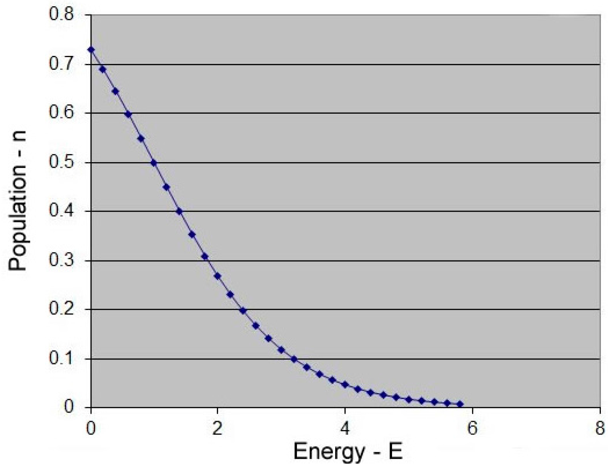
Light emission at the zero-biased LED arises from the random behavior of electrons within their semiconductor materials. Figure 18 shows a generally-accepted distribution of electron energy in semiconductors. It says that some of the electrons have higher energy than average. Carriers are created at the metal contacts, and some of them acquire enough energy from the lattice to reach the direct recombination regions of the LED, where they release some of their energy as a photon. The LED must cool to reflect this energy loss, but is rewarmed from its environment. Thus, heat is converted to light.
4.3. Doped Semiconductor Structure (ATEC)
Our measurements for voltage across an ATEC show consistently (absolute) positive results.
Operation of an ATEC starts with “churning” of carriers (dynamic equilibrium) at a heterojunction of semiconductors of differing intrinsic carrier densities. Churning is our term for what must be happening at the heterojunction. We have not measured it directly (only indirectly through ATEC performance). Physics does not talk about it much (there has been no apparent reason to). Yet, it has to be happening because:
- Generation in a semiconductor material at a given temperature is a function of the bandgap.
- The recombination rate in a semiconductor material is a function of carrier density and band structure.
- Generation and recombination produce an intrinsic (equilibrium) carrier density, which is a function of the bandgap and band structure.
- Some materials have band structures that support higher carrier densities than others, independent of the bandgap.
- Carriers move by diffusion from higher density to lower density regions (given no electrical force on them), including across a heterojunction.
- If two materials with different band structures are joined at a heterojunction, the transport across the junction will typically be out of equilibrium with the internal generation/recombination equilibrium of each material.
- Each material will move to balance at its intrinsic density (for a given temperature) through a change in rate of recombination.
We have a numerical model for the flow of carriers in churning, thanks to Yang et al., 1993 [11]. They only identify the transport model, not the full process with generation and recombination.
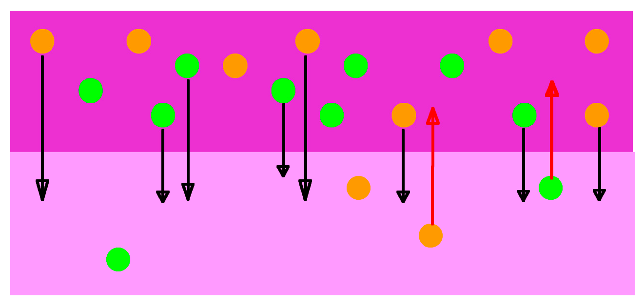
Graphically, churning might look like this: Figure 19 is a simple representation of semiconductors with differing intrinsic densities, not joined.
Figure 20 depicts the results of diffusion as the differing semiconductor materials are joined. Immediately, some of the carriers diffuse to the other material. It is exaggerated for explanatory purposes, showing one half of carriers moving across. The point is that density differences (resulting from band structure) drive the net flow.
As diffusion occurs, carrier densities change. Generation in each semiconductor continues, essentially unaffected by density change. Recombination drops in the higher density material as carriers diffuse away and rises in the lower density material as carriers arrive. Thus, each semiconductor responds to restore it to its intrinsic density. Diffusion continues. Generation and recombination continues. We call this continuous cycle “churning”.
We can calculate the net flow of carriers from high carrier density to low carrier density materials that we used in ATEC prototypes, AlGaAs with 0.5 and 0.33 Al, respectively, based on Yang et al. [11]. The following equations from the paper for electron and hole motion are evaluated in Table 1.
Material values are from Silvaco’s ATLAS, except for affinity, where we used the 60/40 rule.
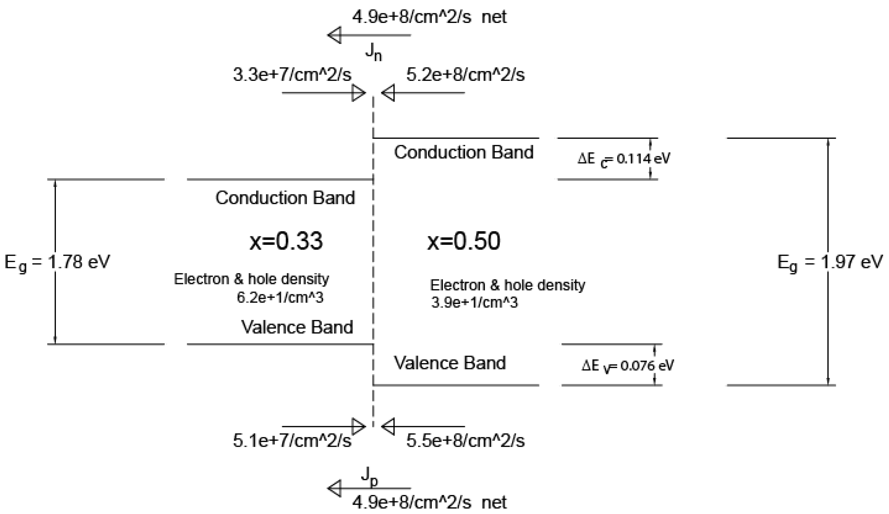
We can relate the current of an ATEC prototype with the current computed above. Net Jn and Jp are nearly equal in count at about 4.9 × 10⁷ carriers per cm2 s or about 7.9 × 10⁻¹¹ A/cm2. Because the charges are opposite, this works out to roughly zero net current. The prototype area is about 35 cm2, and the current was about 2.3 × 10⁻¹¹ A or 6.5 × 10⁻¹² A/cm2. The lower prototype current is accounted for in part by the effect of doped layers and the limited thickness of x = 0.50 layers. Figure 21 below relates these quantities.
For churning, we further note that:
- While there is a flow of carriers, there is no net flow of charge.
- There must be a flow of heat in the opposite direction of carriers, since generation is endothermic and recombination is exothermic. Because this creates a temperature differential, it is in itself an exception to the second law. The temperature difference measurement was cited by George Levy [12], which references offsets encountered by Iwanaga et al. [13].
- This is a generally useless and sometimes annoying feature of heterojunctions (so far).
Here is another way of looking at churning, as though a temperature phenomenon. Let us imagine that the carrier density difference was the result of a temperature difference, rather than a band structure difference. Effectively, a material with a higher C acts as if it is hotter than a material with a lower C. From the intrinsic carrier density:
n*p = C*T3*exp(−Eg/kB*T)
Let us suppose the currents are the result of different carrier densities in the same material due to different temperatures. What temperature would produce the same current ratio?
where T0 = 310 K, Eg is 1.78 eV (for x = 0.33) and the currents are taken from Table 1. Solving numerically, we get a temperature of 334.5 K.
(n*p)/(n0*p0) = (Jn*Jp)/(Jn0*Jp0) = C0*T3*exp(−Eg0/kB*T)/C0*T03*exp(−Eg0/kB*T0)
Given a temperature difference, we can use the Seebeck effect across interposed doped layers to produce a voltage, as shown in Figure 22. This is done using doping to control the Seebeck coefficient: p-doping giving a positive coefficient, such that holes flow from “hot” to “cold”, and n-doping, giving the reverse effect (similar to a hot point probe).
In the AlGaAs sample, most of the ratio is taken up by the exponent term. For x = 0.33 at 310 K, the exponent is −66, so a small percentage change in the exponent has a large change in the value. For our HgCdTe models, the exponent is less than −10, which results in much larger effective temperature differences.
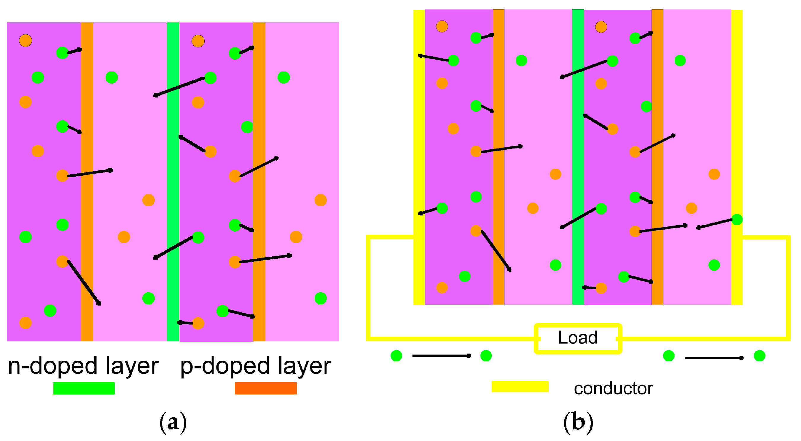
We made a semiconductor sandwich of high and low density semiconductors, with alternate n-doped and p-doped layers between, as shown in Figure 23. The carriers try to churn, but the doping forces electrons only to the left and holes only to the right, as shown in Figure 23a. After an initial surge of churning, a balance is reached (like that which creates a built-in potential in an LED), but there is no net flow across layers because carriers have nowhere to go. If the sandwich has a conductor layer added at each end and connected, electrons may flow from the left conductor, through a load, to the right conductor, as shown in Figure 23b.
5. Conclusions
We have presented experimental results from three systems, each of which indicates that those systems draw heat from their environments and turn it into harvestable work. While the LED direct film exposure experiment is admittedly light, the other experiments were serious, careful work. Each of them contributes to the picture that we need to move from laws to relevant models:
- Epicatalysis created a harvestable temperature difference. That, alone, is enough to prove we must move past laws.
- The light emitted by unbiased LEDs, as captured by the experiments, could in theory be harvested. While not as dramatic as epicatalysis, it also proves the point.
- Consistent voltage measurements from a doped semiconductor structure also demand looking forward.
We believe that implementing demons and ratchets is possible. We believe the open question now is whether it leads to practical results. There may be many more ways to implement them; Figure 1 should prove a useful tool for hunting them.
5.1. Interpretation
We see a huge practical potential for the ATEC. Let us look at some numbers to see where this might go.
- For AlGaAs, the largest bandgap that we used in the ATEC construction is 1.79 eV.
- The test results for our AlGaAs prototypes are, we think, significant. However, they do not scream “useful”. We remind you that we used AlGaAs because many shops could fabricate it.
But consider HgCdTe (Mercat), for which we are looking at a largest bandgap of 0.21 eV.
With Mercat, it should be possible to achieve about 1013 improvement in output or kilowatts per cubic centimeter of the layered material. It is enough that the limiting factor is heat transport into the lattice. In terms of power output, it does not look like a battery so much as a thermally-charged capacitor, able to release rapidly its thermal energy down to a low temperature. Production costs may reach as low as pennies per watt capacity.
5.2. Areas for Research and for Engineering
There is much work to do to bring to life the principles identified. We see:
- Replicating experiments in epicatalysis, LEDs and ATECs;
- Using better material sets for ATECs and lower temperature epicatalysis;
- Developing application-specific packages at least for ATECs (largely an engineering process);
- Looking for other instances of particle creation and destruction, coupled with opportunities for the diffusion of particles (demons and ratchets), for other useful exceptions to the second law.
Supplemental Materials
The following is available online at www.mdpi.com/1099-4300/19/1/34/s1. A Report on Testing of ThermaWatts Prototype Ambient Thermal Electric Converter Devices, V1.1, Peter Orem, 12/2013.
Acknowledgements
Funding for this work came from Frank and Judy Orem and from Peter Orem. Princeton Instruments has graciously loaned cameras to us. We have received questions and ideas from the Oregon State University Physics Department.
Author Contributions
Peter Orem was the major contributor to this work, from conception to test methods and testing. Frank Orem contributed suggestions on testing and was the principal writer.
Conflicts of Interest
The authors declare no conflict of interest.
References
- Nikulov, A.V.; Sheehan, D.P. Special Issue on Quantum Limits to the Second Law of Thermodynamics. Entropy 2004, 6, 1–10. [Google Scholar] [CrossRef]
- Sheehan, D.P. Second law of thermodynamics: Status and challenges. In Proceedings of the AIP Conference, San Diego, CA, USA, 14–15 June 2011.
- ThermaWatts, LLC. Available online: http://www.ThermaWatts.com (accessed on 11 January 2017).
- Sheehan, D.P. Nonequilibrium heterogenous catalysis in long term mean-free-path regime. Phys. Rev. E 2013, 88, 032125. [Google Scholar] [CrossRef] [PubMed]
- Sheehan, D.P.; Garamella, J.T.; Mallin, D.J.; Sheehan, W.F. Steady-state non-equilibrium temperature gradients in hydrogen gas-metal systems: Challenging the second law of thermodynamics. Phys. Scr. 2012, 2012, 014030. [Google Scholar] [CrossRef]
- Sheehan, D.P.; Mallin, D.J.; Garamella, J.T.; Sheehan, W.F. Experimental Test of a Thermodynamic Paradox. Found. Phys. 2014, 44, 235–247. [Google Scholar] [CrossRef]
- Miller, D. Apparatus and Procedures for Detecting Temperature Differentials with Epicatalytic Materials. Entropy 2017. submitted. [Google Scholar]
- Santhanam, P.; Gray, D.J.; Ram, R.J. Thermoelectrically pumped light emitting diodes operating above unity efficiency. Phys. Rev. Lett. 2012, 108, 097403. [Google Scholar] [CrossRef] [PubMed]
- Gray, D. Thermal Pumping of Light Emitting Diodes. Master’s Thesis, Massachusetts Institute of Technology, Cambridge, MA, USA, 2011. [Google Scholar]
- Santhanam, P.; Dodd, J.G.; Ram, R.J. Thermo-Electrically Pumped Light-Emitting Diodes. U.S. Patent US 20140159582, 12 June 2014. [Google Scholar]
- Yang, K.Y.; East, J.R.; Haddad, G.I. Numerical Modeling of Abrupt Heterojunctions Using a Thermionic-Field Emission Boundary Condition. Solid State Electron. 1993, 36, 321–330. [Google Scholar] [CrossRef]
- Levy, G.S. Thermoelectric Effects under Adiabatic Conditions. Entropy 2013, 15, 4700–4715. [Google Scholar] [CrossRef]
- Iwanaga, S.; Toberer, E.S.; LaLonde, A.; Snyder, G.J. A High Temperature Apparatus for Measurement of Seebeck Coefficient. Rev. Sci. Instrum. 2011, 82, 063905. [Google Scholar] [CrossRef] [PubMed]
Figure 1.
A cycle that would create a second law exception.

Figure 2.
Apparatus for recording photons from unbiased LEDs.

Figure 3.
Apparatus for recording from heated LED.

Figure 4.
Prototype ambient thermal electric converter (ATEC).

Figure 5.
ATEC with sweeping voltage source.
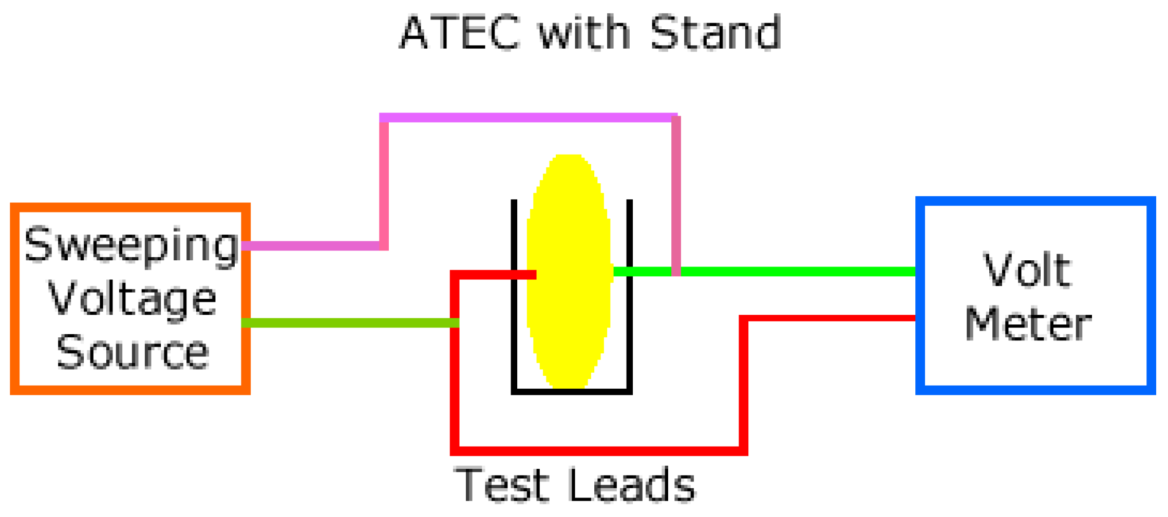
Figure 6.
Test jig.

Figure 7.
Test jig circuitry.

Figure 8.
Sample test jig apparatus.
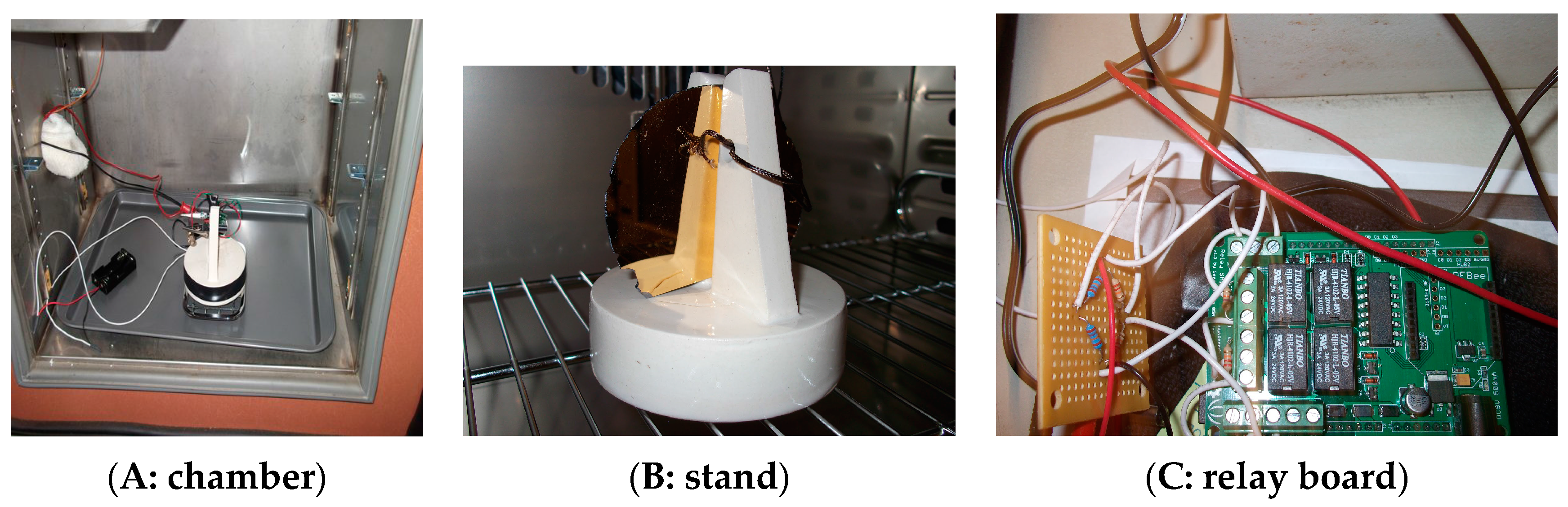
Figure 9.
Film exposed to shorted LED.

Figure 10.
Images from experiment on digital imaging of heated LED. Red Arrows touch rectangular base of LED, lens is above arrow tip.
Figure 10.
Images from experiment on digital imaging of heated LED. Red Arrows touch rectangular base of LED, lens is above arrow tip.

Figure 11.
Modeled flow of electrons and holes.
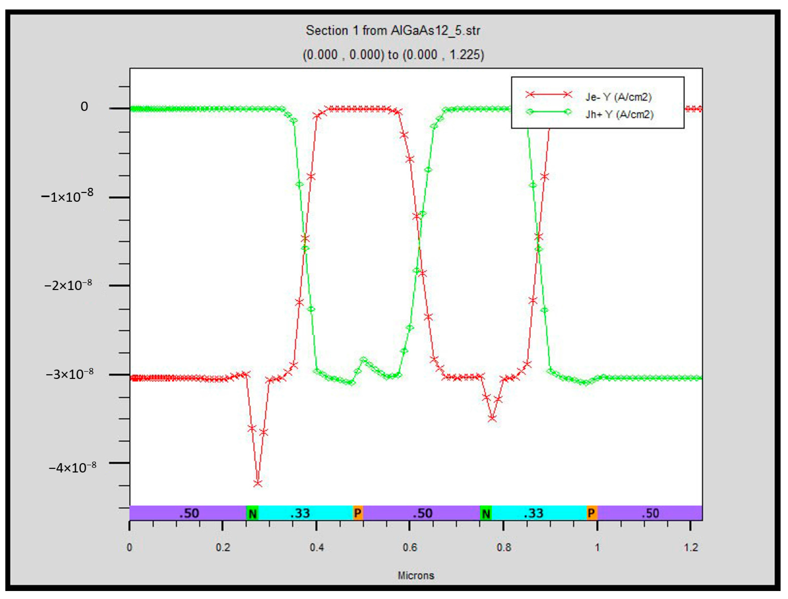
Figure 12.
Current/Voltage Plot for ATEC R2 Prototype at 120 °F.

Figure 13.
Current vs. Voltage Plot for ATEC R2 Prototype and resistors at 160 °F.
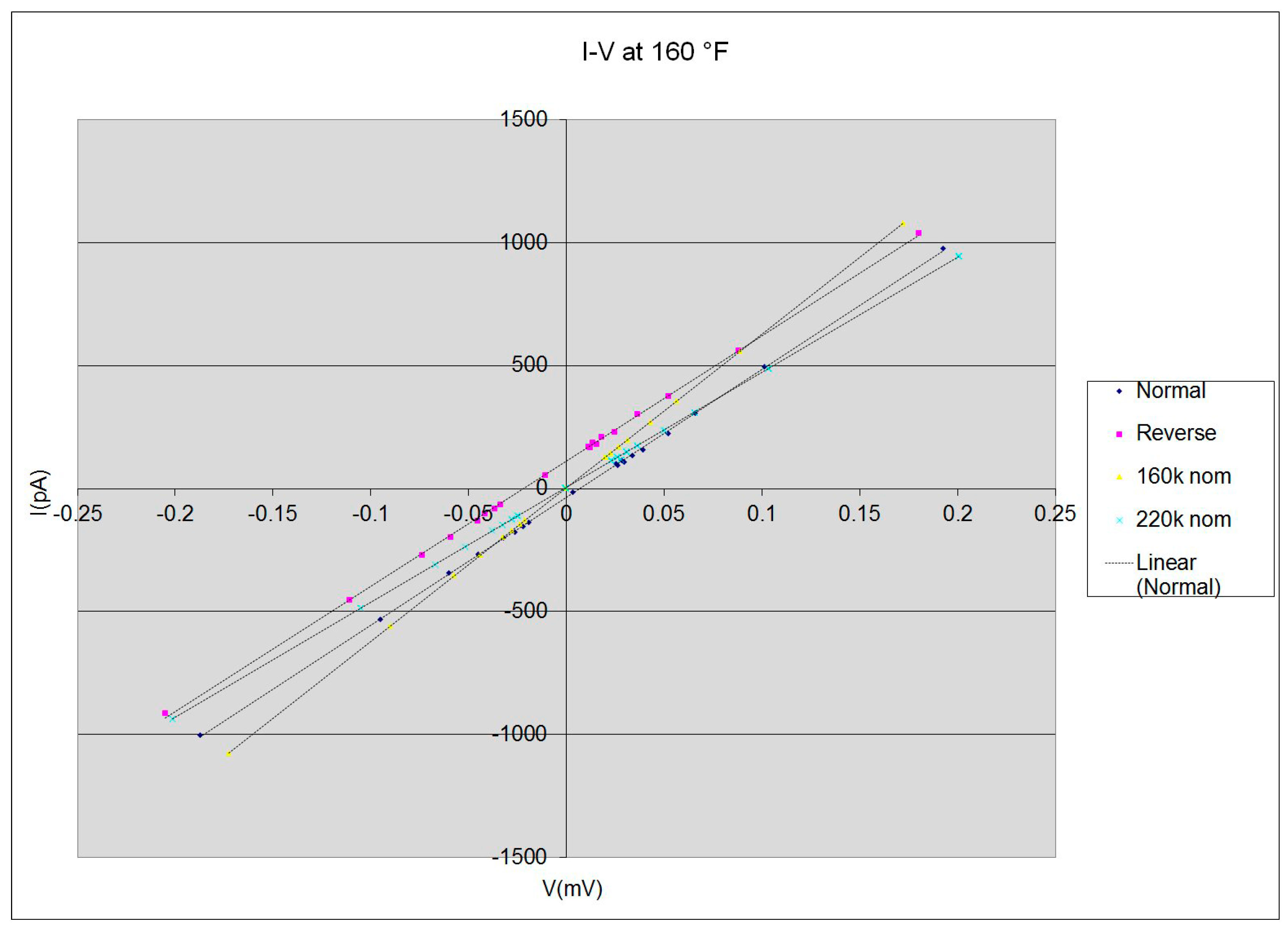
Figure 14.
A view of epicatalysis.

Figure 15.
Setup for epicatalysis tests. (a) Overview of test bed heating and temperature measurement; (b) Detail with catalytic surfaces inside chamber. Have got the permission of Springer.
Figure 15.
Setup for epicatalysis tests. (a) Overview of test bed heating and temperature measurement; (b) Detail with catalytic surfaces inside chamber. Have got the permission of Springer.
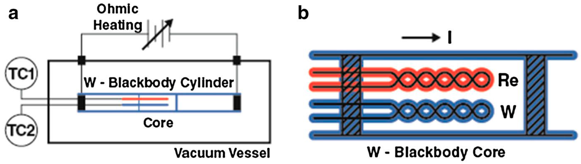
Figure 16.
Temperature differences between catalysts [6]. Have got the permission of Springer.
Figure 16.
Temperature differences between catalysts [6]. Have got the permission of Springer.

Figure 17.
Over-unity efficiency of LED near zero bias [10].
Figure 17.
Over-unity efficiency of LED near zero bias [10].
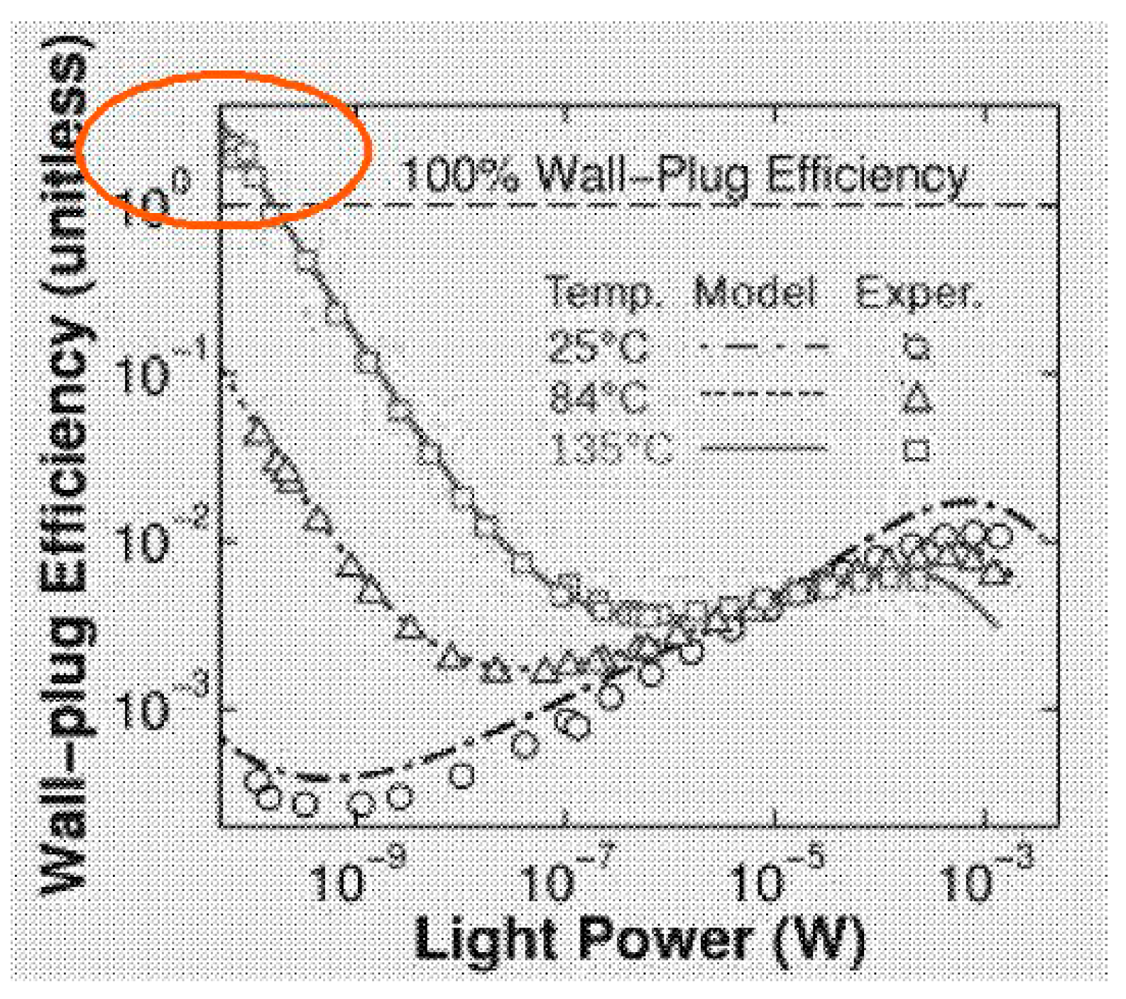
Figure 18.
Distribution of electron energy (Fermi–Dirac).

Figure 19.
Semiconductors of different intrinsic carrier densities.
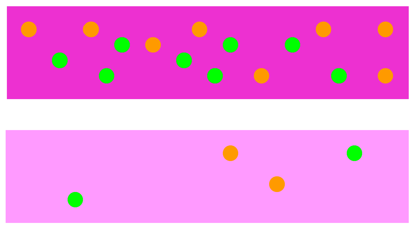
Figure 20.
Diffusion across a heterojunction.

Figure 21.
AlGaAs Heterojunction Bands and Currents.

Figure 22.
Seebeck effect across doped layers.
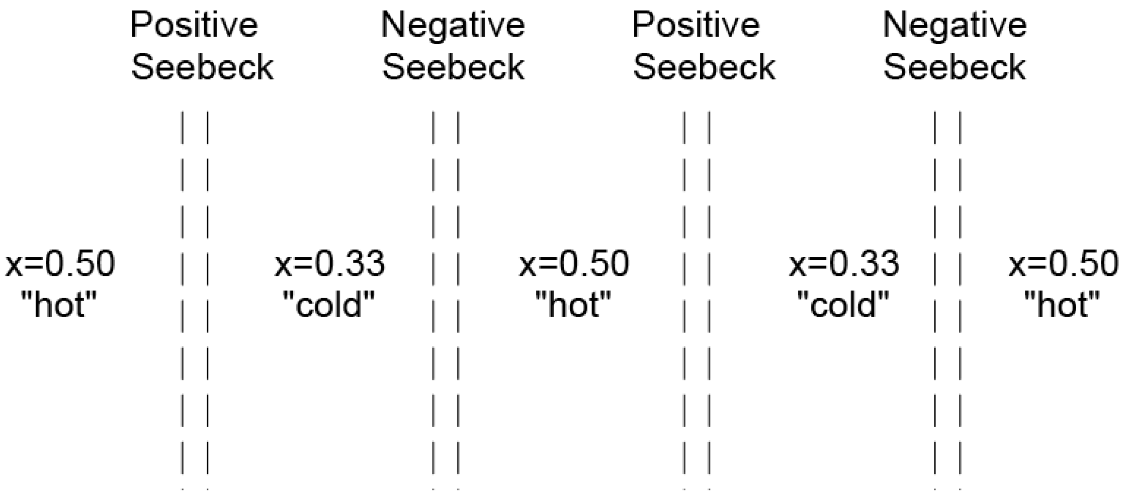
Figure 23.
Churning with doped layers. (a) High and low density layers with n-doped and p-doped layers added; (b) Complete assembly of layers with contacts and load added.
Figure 23.
Churning with doped layers. (a) High and low density layers with n-doped and p-doped layers added; (b) Complete assembly of layers with contacts and load added.


| Al Fractions | Units | Notes and References | |||
|---|---|---|---|---|---|
| 0.33 | 0.5 | - | - | ||
| ni | 3.82 × 10³ | 1.52× 10³ | /cm3 | Carrier density at 310 K, per ATLAS | |
| Eg | 1.78 | 1.97 | 0.19 | eV | Per ATLAS |
| ∆Ec | - | 0.6 | 0.114 | eV | 60/40 rule for AlGaAs |
| ∆Ev | - | 0.4 | 0.076 | eV | 60/40 rule for AlGaAs |
| kBT | - | - | 0.0267138 | eV | kB from ATLAS |
| ∆Ec/kBT | - | - | 4.27 | - | - |
| ∆Ev/kBT | - | - | 2.84 | - | - |
| exp(∆Ec/kBT) | - | - | 1.40 × 10⁻² | - | - |
| exp(∆Ev/kBT) | - | - | 5.81 × 10⁻² | - | - |
| vn | 3.86 × 10⁷ | 1.34 × 10⁸ | - | cm/s | Yang [11] Equations (5) and (9) |
| vp | 1.42 × 10⁷ | 1.40 × 10⁸ | - | cm/s | Yang [11] Equations (12) and (13) |
| Densities | - | - | - | - | - |
| n | 6.18 × 10 | 3.90 × 10 | - | /cm3 | - |
| p | 6.18× 10 | 3.90 × 10 | - | /cm3 | - |
| Currents | - | - | Net | - | - |
| Jn | −3.34 × 10⁷ | 5.22 × 10⁸ | 4.89 × 10⁸ | /cm2/s | Net of 0.33 => 0.50 minus 0.50 => 0.33 for electrons |
| Jp | 5.10 × 10⁷ | −5.46 × 10⁸ | −4.95 × 10⁸ | /cm2/s | Net of 0.33 => 0.50 minus 0.50 => 0.33 for holes |
© 2017 by the authors; licensee MDPI, Basel, Switzerland. This article is an open access article distributed under the terms and conditions of the Creative Commons Attribution (CC-BY) license (http://creativecommons.org/licenses/by/4.0/).
Share and Cite
MDPI and ACS Style
Orem, P.M.; Orem, F.M. Implementing Demons and Ratchets. Entropy 2017, 19, 34. https://doi.org/10.3390/e19010034
AMA Style
Orem PM, Orem FM. Implementing Demons and Ratchets. Entropy. 2017; 19(1):34. https://doi.org/10.3390/e19010034
Chicago/Turabian StyleOrem, Peter M., and Frank M. Orem. 2017. "Implementing Demons and Ratchets" Entropy 19, no. 1: 34. https://doi.org/10.3390/e19010034
Note that from the first issue of 2016, this journal uses article numbers instead of page numbers. See further details here.