High Photoelectric Conversion Efficiency of Metal Phthalocyanine/Fullerene Heterojunction Photovoltaic Device

Abstract
:1. Introduction
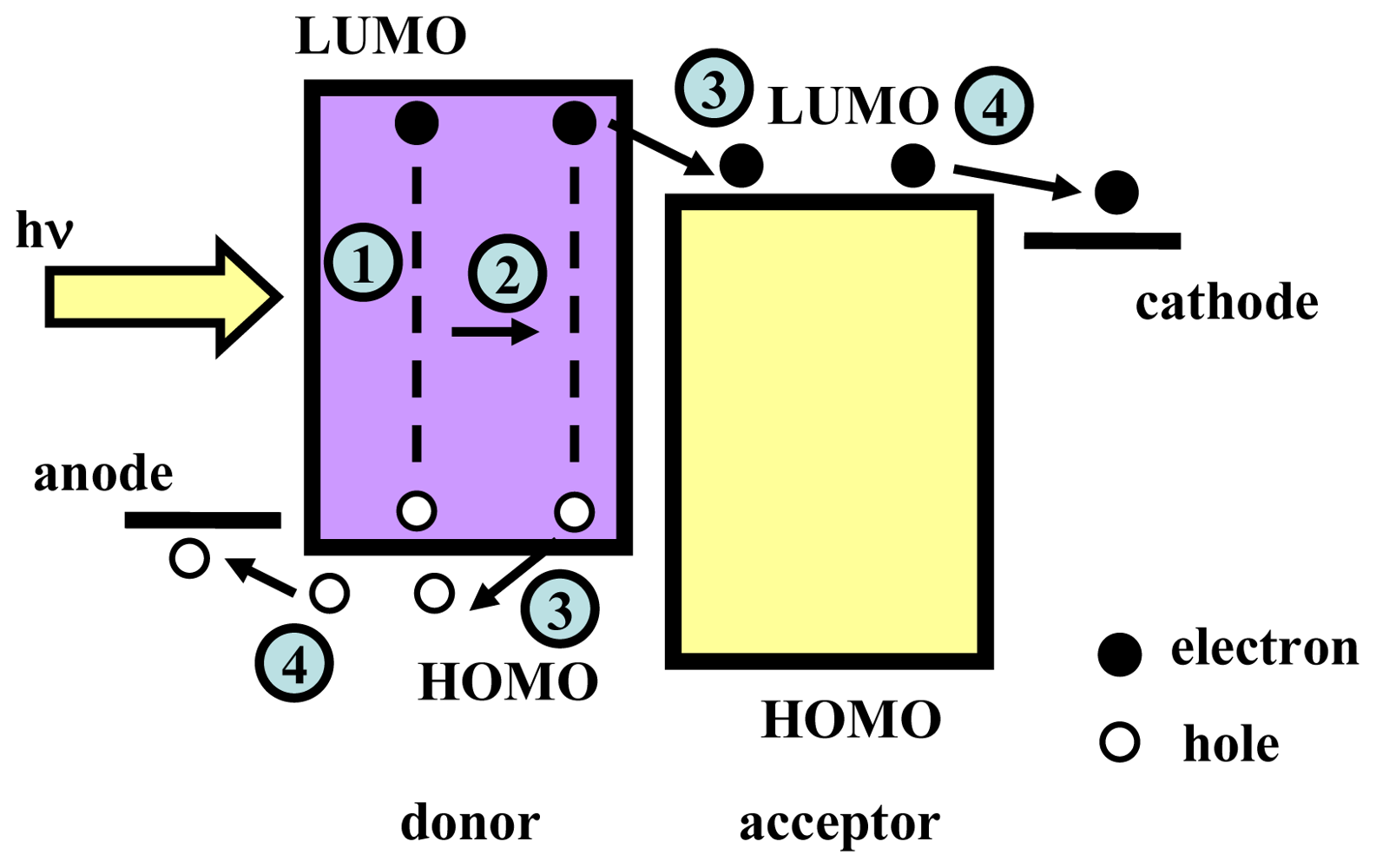
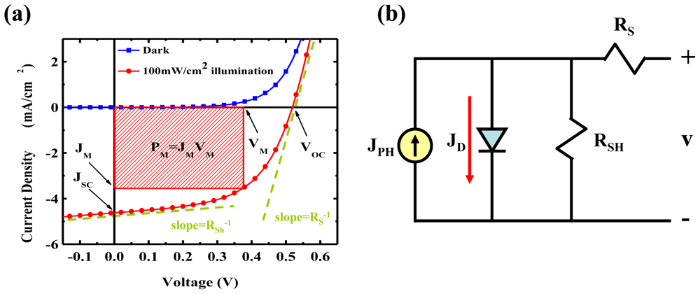
2. Principle of OPV
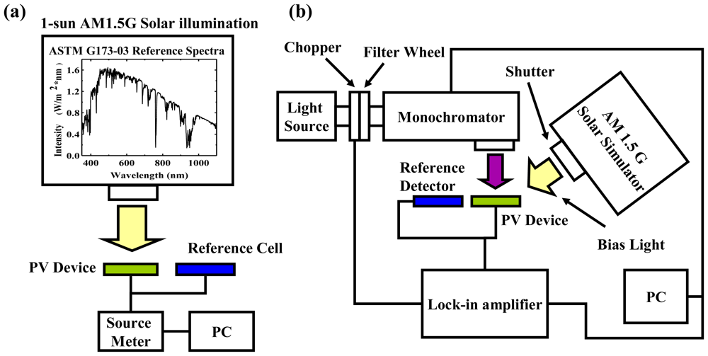
3. Experimental: Device Fabrication and Measurement
4. Efficiency Improvement Techniques
4.1. Electrode Modifications
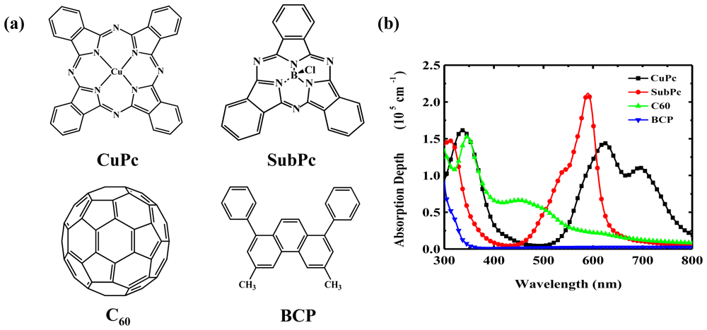
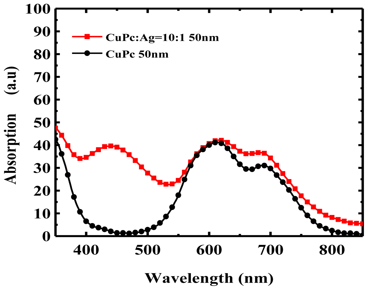
4.2. Active Layer
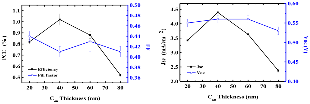
4.3. Thickness of the Active Layer
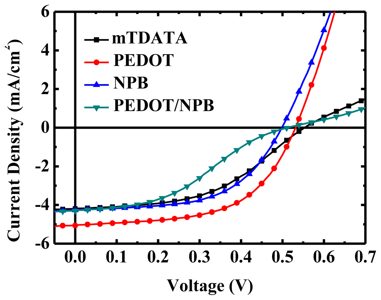
4.4. Injection and Transporting Layer
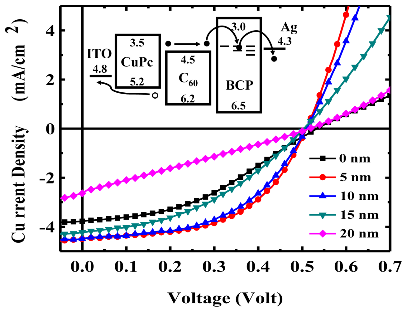
4.5. Exciton Blocking Layer
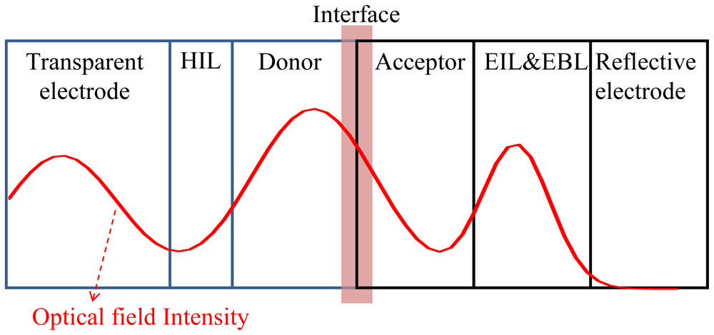
4.6. Internal Optics
4.7. External Optics
5. Conclusions
Acknowledgements
References
- Service, RF. Is It Time to Shoot for the Sun? Science 2005, 309, 548. [Google Scholar]
- Green, MA; Emery, K; Hishikawa, Y; Warta, W. Solar cell efficiency tables (version 35). Prog. Photovolt: Res. Appl 2010, 18, 144–150. [Google Scholar]
- Shockley, W; Queisser, HJ. Detailed balance limit of efficiency of p-n junction solar cells. J. Appl. Phys 1961, 32, 510–519. [Google Scholar]
- Grätzel, M. Solar energy conversion by dye-sensitized photovoltaic cells. Inorg. Chem 2005, 44, 6841. [Google Scholar]
- Tang, CW. Two-layer organic photovoltaic cell. Appl. Phys. Lett 1986, 48, 183–185. [Google Scholar]
- Yu, G; Gao, J; Hummelen, JC; Wudl, F; Heeger, AJ. Polymer photovoltaic cells: Enhanced efficiencies via a network of internal donor-acceptor heterojunctions. Science 1995, 270, 1789–1791. [Google Scholar]
- Nelson, J. Organic photovoltaic films. Curr. Opin. Solid State Mater. Sci 2002, 6, 87–95. [Google Scholar]
- Granström, M; Petritsch, K; Arias, AC; Lux, A; Andersson, MR; Friend, RH. Laminated fabrication of polymeric photovoltaic diodes. Nature 1998, 395, 257–260. [Google Scholar]
- Peumans, P; Bulović, V; Forrest, SR. efficient photon harvesting at high optical intensities in ultrathin organic double-heterostructure photovoltaic diodes. Appl. Phys. Lett 2000, 76, 2650–2652. [Google Scholar]
- Chan, MY; Lai, SL; Fung, MK; Lee, CS; Lee, ST. Doping-induced efficiency enhancement in organic photovoltaic devices. Appl Phys Lett 2007, 90. [Google Scholar]
- Tsuzuki, T; Shirota, Y; Rostalski, J; Meissner, D. The effect of fullerene doping on photoelectric conversion using titanyl phthalocyanine and a perylene pigment. Sol. Energy Mater. Sol Cells 2000, 61, 1–8. [Google Scholar]
- Yakimov, A; Forrest, SR. High photovoltage multiple-heterojunction organic solar cells incorporating interfacial metallic nanoclusters. Appl. Phys. Lett 2002, 80, 1667–1669. [Google Scholar]
- Drechsel, J; Männig, B; kozlowski, F; Pfeiffer, M; Leo, K; Hoppe, H. Efficient organic solar cells based on a double p-i-n architecture using doped wide-gap transport layers. Appl Phys Lett 2005, 86. [Google Scholar]
- Chen, H-Y; Hou, J; Zhang, S; Liang, Y; Yang, G; Yang, Y; Yu, L; Wu, Y; Li, G. Polymer solar cells with enhanced open-circuit voltage and efficiency. Nature Photon 2009, 3, 649–653. [Google Scholar]
- Johnev, B; Vogel, M; Fostiropoulos, K; Mertesacker, B; Rusu, M; Lux-Steiner, M-C; Weidinger, A. Monolayer passivation of the transparent electrode in organic solar cells. Thin Solid Films 2005, 488, 270–273. [Google Scholar]
- Hong, ZR; Liang, CJ; Sun, XY; Zeng, XT. Characterization of organic photovoltaic devices with indium-tin-oxide anode treated by plasma in various gases. J Appl Phys 2006, 100. [Google Scholar]
- Rand, BP; Xue, J; Yang, F; Forrest, SR. Organic solar cells with sensitivity extending into the near infrared. Appl Phys Lett 2005, 87. [Google Scholar]
- Hong, ZR; Maennig, B; Lessmann, R; Pfeiffer, M; Leo, K; Simon, P. Improved efficiency of zinc phthalocyanine/C60 based photovoltaic cells via nanoscale interface modification. Appl Phys Lett 2007, 90. [Google Scholar]
- Sista, S; Yao, Y; Yang, Y; Tang, ML; Bao, Z. Enhancement in open circuit voltage through a cascade-type energy band structure. Appl Phys Lett 2007, 91. [Google Scholar]
- Dai, J; Jiang, X; Wang, H; Yan, D. Organic photovoltaic cells with near infrared absorption spectrum. Appl Phys Lett 2007, 91. [Google Scholar]
- Yang, F; Lunt, RR; Forrest, SR. Simultaneous heterojunction organic solar cells with broad spectral sensitivity. Appl Phys Lett 2008, 92. [Google Scholar]
- Zhang, G; Li, W; Chu, B; Chen, L; Yan, F; Zhu, J; Chen, Y; Lee, CS. Cascade-energy level alignment based organic photovoltaic cells by utilizing copper phthalocyanine as bipolar carrier transporting layer. Appl Phys Lett 2009, 94. [Google Scholar]
- Kumar, H; Kumar, P; Bhardwaj, R; Sharma, GD; Chand, S; Jain, SC; Kumar, V. Broad spectral sensitivity and improved efficiency in CuPc/Sub-Pc organic photovoltaic devices. J Phys D: Appl Phys 2009, 42. [Google Scholar]
- Li, N; Lassiter, BE; Lunt, RR; Wei, G; Forrest, SR. Open circuit voltage enhancement due to reduced dark current in small molecule photovoltaic cells. Appl Phys Lett 2009, 94. [Google Scholar]
- Chauhan, KV; Sullivan, P; Yang, JL; Jones, TS. Efficient organic photovoltaic cells through structural modification of chloroaluminum phthalocyanine/fullerene heterojunctions. J. Phys. Chem C 2010, 114, 3304–3308. [Google Scholar]
- Wu, J; Becerril, HA; Bao, Z; Liu, Z; Chen, Y; Peumans, P. Organic solar cells with solutionprocessed graphene transparent electrodes. Appl Phys Lett 2008, 92. [Google Scholar]
- Murdoch, GB; Hinds, S; Sargent, EH; Tsang, SW; Mordoukhovski, L; Lu, ZH. Aluminum doped zinc oxide for organic photovoltaics. Appl Phys Lett 2009, 94. [Google Scholar]
- Mutolo, KL; Mayo, EI; Rand, BP; Forrest, SR; Thompson, ME. Enhanced open-circuit voltage in subphthalocyanine/C60 organic photovoltaic cells. J. Am. Chem. Soc 2006, 128, 8108–8109. [Google Scholar]
- Bailey-Salzman, RF; Rand, BP; Forrest, SR. Near-infrared sensitive small molecule organic photovoltaic cells based on chloroaluminum phthalocyanine. Appl Phys Lett 2007, 91. [Google Scholar]
- Tong, X; Lassiter, BE; Forrest, SR. Inverted organic photovoltaic cells with high open-circuit voltage. Org. Electron 2010, 11, 705–709. [Google Scholar]
- Peumans, P; Forrest, SR. Very-high-efficiency double-heterostructure copper phthalocyanine/C60 photovoltaic cells. Appl. Phys. Lett 2001, 79, 126–128. [Google Scholar]
- Chu, CW; Shrotriya, V; Li, G; Yang, Y. Tuning acceptor energy level for efficient charge collection in copper-phthalocyanine-based organic solar cells. Appl Phys Lett 2006, 88. [Google Scholar]
- Rand, BP; Li, J; Xue, J; Homes, RJ; Thompson, ME; Forrest, SR. Organic double-heterostructure photovoltaic cells employing thick tris(acetylacetonato)ruthenium(III) exciton-blocking layers. Adv. Mater 2005, 17, 2714–2718. [Google Scholar]
- Song, QL; Li, FY; Yang, H; Wu, HR; Wang, XZ; Zhou, W; Zhao, JM; Ding, XM; Huang, CH; Hou, XY. Small-molecule organic solar cells with improved stability. Chem. Phys. Lett 2005, 416, 42–46. [Google Scholar]
- Vogel, M; Doka, S; Breyer, Ch; Lux-Steiner, MC; Fostiropoulos, K. On the function of a bathocuproine buffer layer in organic photovoltaic cells. Appl Phys Lett 2006, 89. [Google Scholar]
- Chan, MY; Lai, SL; Lau, KM; Lee, CS; Lee, ST. Application of metal-doped organic layer both as exciton blocker and optical spacer for organic photovoltaic devices. Appl Phys Lett 2006, 89. [Google Scholar]
- Gommans, H; Verreet, B; Rand, BP; Muller, R; Poortmans, J; Heremans, P; Genoe, J. On the role of bathocuproine in organic photovoltaic cells. Adv. Funct. Mater 2008, 18, 3686–3691. [Google Scholar]
- Peumans, P; yakimov, A; Forrest, SR. Small molecular weight organic thin-film photodetectors and solar cells. J. Appl. Phys 2003, 93, 3693–3723. [Google Scholar]
- Koster, LJA; Smits, ECP; Mihailetchi, VD; Blom, PWM. Device model for the poeration of polymer/fullerene bulk heterojunction solar cells. Phys Rev B 2005, 72. [Google Scholar]
- Rand, BP; Burk, DP; Forrest, SR. Offset energies at organic semiconductor heterojunctions and their influence on the open-circuit voltage of thin-film solar cells. Phys Rev B 2007, 75. [Google Scholar]
- Kietzke, T. Recent advances in organic solar cells. Adv. Optoelectron 2007, 2007, 1–15. [Google Scholar]
- Petritsch, K. Organic solar cell architectures. Ph.D. Thesis, Technische Universität Graz, Graz, Austria, 2000. [Google Scholar]
- Rand, BP; Genoe, J; Heremans, P; Poortmans, J. Solar cells utilizing small molecular weight organic semiconductors. Prog. Photovolt: Res. Appl 2007, 15, 659–676. [Google Scholar]
- Forrest, SR. Ultrathin organic films grown by organic molecular beam deposition and related techniques. Chem. Rev 1997, 97, 1793–1896. [Google Scholar]
- Baldo, M; Deutsch, M; Burrow, P; Gossenberger, H; Gerstenberg, M; Ban, V; Forrest, SR. Organic vapor phase deposition. Adv. Mater 1998, 10, 1505–1514. [Google Scholar]
- Shtein, M; Gossenberger, HF; Benziger, JB; Forrest, SR. Material transport regimes and mechanisms for growth of molecular organic thin films using low-pressure organic vapor phase deposition. J. Appl. Phys 2001, 89, 1470–1476. [Google Scholar]
- Yang, F; Sun, K; Forrest, SR. Efficient solar cells using all-organic nanocrystalline networks. Adv. Mater 2007, 19, 4166–4171. [Google Scholar]
- Shrotriya, V; Li, G; Yao, Y; Moriarty, T; Emery, K; Yang, Y. Accurate measurement and characterization of organic solar cells. Adv. Funct. Mater 2006, 16, 2016–2023. [Google Scholar]
- Standard ASTM G173-03. Standard tables for reference solar spectral irradiances: direct normal and hemispherical on 37° tilted surface. Available online: http://www.astm.org/DATABASE.CART/HISTORICAL/G173-03.htm (accessed on 27 December 2010).
- Standard ASTM E927-05. Standard specification for solar simulation for photovoltaic testing. Available online: http://www.astm.org/Standards/E927.htm (accessed on 27 December 2010).
- Standard ASTM E948-05a. Standard test method for electrical performance of photovoltaic cells using reference cells under simulated sunlight. Available online: http://www.astm.org/DATABASE.CART/HISTORICAL/E948-05A.htm (accessed on 27 December 2010).
- Standard ASTM E948-05a. Standard test method for spectral responsivity measurements of photovoltaic devices. Available online: http://www.astm.org/DATABASE.CART/HISTORICAL/E948-05A.htm (accessed on 27 December 2011).
- Brabec, CJ; Cravino, A; Meissner, D; Sariciftci, NS; Fromherz, T; Rispens, MT; Sanchez, L; Hummelen, JC. Origin of the open circuit voltage of plastic solar cells. Adv. Funct. Mater 2001, 11, 374–380. [Google Scholar]
- Kumar, A; Sista, S; Yang, Y. Dipole induced anomalous S-shape I–V curves in polymer solar cells. J Appl Phys 2009, 105. [Google Scholar]
- Mihailetchi, VD; Blom, PWM; Hummelen, JC; Rispens, MT. Cathode dependence of the open-circuit voltage of polymer:fullerene bulk heterojunction solar cells. J. Appl. Phys 2003, 94, 6849–6854. [Google Scholar]
- Pandey, AK; Shaw, PE; Samuel, IDW; Nunzi, J-M. Effect of metal cathode reflectance on the exciton-dissociation efficiency in heterojunction organic solar cells. Appl Phys Lett 2009, 94. [Google Scholar]
- Hains, AW; Marks, TJ. High-efficiency hole extraction electron-blocking layer to replace poly(3,4-ethylenedioxythiophene):poly(styrene sulfonate) in bulk-heterojunction polymer solar cells. Appl Phys Lett 2008, 92. [Google Scholar]
- Boer, B; Hadipour, A; Mandoc, MM; Woudenbergh, T; Blom, PWM. Tuning of metal work functions with self-assembled monolayers. Adv. Mater 2005, 17, 621–625. [Google Scholar]
- Irwin, MD; Buchholz, DB; Hains, AW; Chang, RPH; Marks, TJ. p-type semiconducting nickel oxide as an efficiency-enhancing anode interfacial layer in polymer bulk-heterojunction solar cells. Proc. Natl. Acad. Sci USA 2008, 105, 2783–2787. [Google Scholar]
- Chang, C-C; Lin, C-F; Chiou, J-M; Ho, T-H; Tai, Y; Lee, J-H; Chen, Y-F; Wang, J-K; Chen, L-C; Chen, K-H. Effects of cathode buffer layers on the efficiency of bulk-heterojunction solar cells. Appl Phys Lett 2010, 96. [Google Scholar]
- Camacho, JM; Oliva, AI. Surface and grain boundary contributions in the electrical resistivity of metallic nanofilms. Thin Solid Films 2006, 515, 1881–1885. [Google Scholar]
- Lee, J-Y; Connor, ST; Cui, Y; Peumans, P. Solution-processed metal nanowire mesh transparent electrodes. Nano Lett 2008, 8, 689–692. [Google Scholar]
- O’Connor, B; Haughn, C; An, K-H; Pipe, KP; Shtein, M. Transparent and conductive electrodes based on unpatterned, thin metal films. Appl Phys Lett 2008, 93, 223304:1–223304:3. [Google Scholar]
- Chen, Z; Cotterell, B; Wang, W; Guenther, E; Chua, S-J. A mechanical assessment of flexible optoelectronic devices. Thin Solid Films 2001, 394, 202–206. [Google Scholar]
- Forrest, SR. The path to ubiquitous and low-cost organic electronic appliances on plastic. Nature 2004, 428, 911–918. [Google Scholar]
- Lee, ST; Gao, ZQ; Hung, LS. Metal diffusion from electrodes in organic light-emitting diodes. Appl. Phys. Lett 1999, 75, 1404–1406. [Google Scholar]
- Wong, KW; Yip, HL; Luo, Y; Wong, KY; Lau, WM; Low, KH; Chow, HF; Gao, ZQ; Yeung, WL; Chang, CC. Blocking reactions between indium-tin oxide and poly (3,4-ethylene dioxythiphene):poly(styrene sulphonate) with a self-assembly monolayer. Appl. Phys. Lett 2002, 80, 2788–2790. [Google Scholar]
- Schulze, K; Maennig, B; Lao, K; Tomita, Y; May, C; Hüpkes, J; Brier, E; Reinold, E; Bäuerle, P. Organic solar cells on indium tin oxide and aluminum doped zinc oxide anodes. Appl Phys Lett 2007, 91. [Google Scholar]
- Murdoch, GB; Hinds, S; Sargent, EH; Tsang, SW; Mordoukhovski, L; Lu, ZH. Aluminum doped zinc oxide for organic photovoltaics. Appl Phys Lett 2009, 94. [Google Scholar]
- Park, YR; Jung, D; Kim, YS. Organic solar cells with hydrogenated in-doped ZnO replacing Sn-doped In2O3 as transparent electrode. Jpn. J. Appl. Phys 2008, 47, 516–520. [Google Scholar]
- Groenendaal, LB; Jonas, F; Freitag, D; Pielartzik, H; Reynolds, JR. Poly(3,4-ethylenedioxythiophene) and its derivatives: past, present, and future. Adv. Mater 2000, 12, 481–494. [Google Scholar]
- Ago, H; Petritsch, K; Shaffer, MSP; Windle, AH; Friend, RH. Composites of carbon nanotubes and conjugated polymers for photovoltaic devices. Adv. Mater 1999, 11, 1281–1285. [Google Scholar]
- Zhang, M; Fang, S; Zakhidov, AA; Lee, SB; Aliev, AE; Wiiliams, CD; Atkinson, KR; Baughman, RH. Strong, transparent, multifunctional, carbon nanotube sheets. Science 2005, 309, 1215–1219. [Google Scholar]
- Weeks, C; Levitsky, I; Peltola, J; Glatkowski, P. Organic solar cells with carbon nanotubes replacing In2O3:Sn as the transparent electrode. Appl Phys Lett 2006, 88. [Google Scholar]
- Rowell, MW; Topinka, MA; McGehee, MD; Prall, H-J; Dennler, G; Sariciftci, NS. Organic solar cells with carbon nanotube network electrodes. Appl Phys Lett 2006, 88. [Google Scholar]
- Wang, X; Zhi, L; Müllen, K. Transparent, conductive graphene electrodes for dye-sensitized solar cells. Nano Lett 2008, 8, 323–327. [Google Scholar]
- Tseng, C-T; Cheng, Y-H; Lee, MCM; Han, C-C; Cheng, C-H; Tao, Y-T. Study of anode work function modified by self-assembled monolayers on pentacene/fullerene organic solar cells. Appl Phys Lett 2007, 91. [Google Scholar]
- Meiss, J; Allinger, N; Riede, MK; Leo, K. Improved light harvesting in tin-doped indium oxide (ITO)-free inverted bulk-heterojunction organic solar cells using capping layers. Appl Phys Lett 2008, 93. [Google Scholar]
- Meiss, J; Riede, MK; Leo, K. Towards efficient tin-doped indium oxide (ITO)-free inverted organic solar cells using metal cathodes. Appl Phys Lett 2008, 94. [Google Scholar]
- Meiss, J; Furno, M; Pfuetzner, S; Leo, K; Riede, M. Selective absorption enhancement in organic solar cells using light incoupling layers. J Appl Phys 2010, 107. [Google Scholar]
- Lin, CF; Liu, SW; Hsu, WF; Zhang, M; Chiu, TL; Wu, Y; Lee, JH. Modification of Silver Anode and Cathode for Top-illuminated Organic Photovoltaic Device. J. Phys. D: Appl. Phys 2010, 43, 395101. [Google Scholar]
- Claessens, CG; González-Rodriguez, D; Torres, T. Subphthalocyanines: Singular nonplanar aromatic compunds-synthesis, reactivity, and physical properties. Chem. Rev 2002, 102, 835–853. [Google Scholar]
- Roman, LS; Mammo, W; Pettersson, LAA; Andersson, MR; Inganäs, O. High quantum efficiency polythiophene/C60 photodiodes. Adv. Mater 1998, 10, 774–777. [Google Scholar]
- Halls, JJM; Pichler, K; Friend, RH; Moratti, SC; Homes, AB. Exciton dissociation at a poly(p-phenylenevinylene)/C60 heterojunction. Synth. Met 1996, 77, 277–280. [Google Scholar]
- Pettersson, LAA; Roman, LS; Inganäs, O. Modeling photocurrent action spectra of photovoltaic devices based on organic thin films. J. Appl. Phys 1999, 86, 487–496. [Google Scholar]
- Arbogast, JW; Darmanyan, AP; Foote, CS; Rubin, Y; Diederich, FN; Alvarez, MM; Anz, SJ; Whetten, RL. Photophysical properties of C60. J. Phys. Chem 1991, 95, 11–12. [Google Scholar]
- Arbogast, JW; Foote, CS; Kao, M. Electron transfer to triplet C60. J. Am. Chem. Soc 1992, 114, 2277–2279. [Google Scholar]
- Ma, L; Quyang, J; Yang, Y. High-speed and high-current density C60 diodes. Appl. Phys. Lett 2004, 84, 4786–4788. [Google Scholar]
- Heutz, S; Sullivan, P; Sanderson, BM; Schultes, SM; Jones, TS. influence of molecular architecture and intermixing on the photovoltaic, morphological and spectroscopic properties of CuPc-C60 heterojunctions. Sol. Energy Mater. Sol Cells 2004, 83, 229–245. [Google Scholar]
- Wu, CC; Wu, CI; Sturm, JC; Kanh, A. Surface modification of indium tin oxide by plasma treatment: An effective method to improve the efficiency, brightness, and reliability of organic light emitting devices. Appl. Phys. Lett 1997, 70, 1348–1350. [Google Scholar]
- Xue, J; Uchida, S; Rand, BP; Forrest, SR. 4.2% efficient organic photovoltaic cells with low series resistances. Appl. Phys. Lett 2004, 84, 3013–3015. [Google Scholar]
- Uchida, S; Xue, J; Rand, BP; Forrest, SR. Organic small molecule solar cells with a homogeneously mixed copper phthalocyanine: C60 active layer. Appl. Phys. Lett 2004, 84, 4218–4220. [Google Scholar]
- Brown, TM; Kim, JS; Friend, RH; Cacialli, F; Daik, R; Feast, WJ. Built-in field electroabsorption spectroscopy of polymer light-emitting diodes incorporating a doped poly(3,4-ethylene dioxythiophene) hole injection layer. Appl. Phys. Lett 1999, 75, 1679–1681. [Google Scholar]
- Choulis, SA; Choong, VE; Patwardhan, A; Mathai, MK; So, F. Interface modification to improve hole-injection properties in organic electronic devices. Adv. Funct. Mater 2006, 16, 1075–1080. [Google Scholar]
- Yin, C; Pieper, B; Stiller, B; Kietzke, T; Neher, D. Charge carrier generation and electron blocking at inerlayers in polymer solar cells. Appl Phys Lett 2007, 90. [Google Scholar]
- Murata, K; Ciná, S; Greenham, NC. Barriers to electron extraction in polymer light-emitting diodes. Appl. Phys. Lett 2001, 79, 193–195. [Google Scholar]
- Jong, MP; IJendoorn, LJ; Voigt, MJA. Stability of the interface between indium-tin oxide and poly(3,4-ethylenedioxythiophene)/poly(styrenesulfonate) in polymer light-emitting diodes. Appl. Phys. Lett 2000, 77, 2255–2257. [Google Scholar]
- Shrotriya, V; Li, G; Yao, Y; Chu, C-W; Yang, Y. Transition metal oxides as the buffer layer for polymer photovoltaic cells. Appl Phys Lett 2006, 88. [Google Scholar]
- Song, QL; Li, CM; Wang, ML; Sun, XY; Hou, XY. Role of buffer in organic solar cells using C60 as an acceptor. Appl Phys Lett 2007, 90. [Google Scholar]
- Krebs, FC; Spanggaard, H. Significant improvement of polymer solar cell stability. Chem. Mater 2005, 17, 5235–5237. [Google Scholar]
- Jørgensen, M; Norrman, K; Krebs, FC. Stability/degradation of polymer solar cells. Sol. Energy Mater. Sol Cells 2008, 92, 686–714. [Google Scholar]
- Hong, ZR; Huang, ZH; Zeng, XT. Utilization of copper phthalocyanine and bathocuproine as an electron transport layer in photovoltaic cells with copper phthalocyanine/buckminsterfullerene heterojunctions: Thickness effect on photovoltaic performances. Thin Solid Films 2007, 515, 3019–3023. [Google Scholar]
- Liu, S-W; Lee, C-C; Lin, C-F; Huang, J-C; Chen, C-T; Lee, J-H. 4-Hydroxy-8-methyl-1,5-naphthyridine aluminium chelate: a mohrphologically stable and efficient exciton-blocking material for organic photovoltaics with prolonged lifetime. J. Mater. Chem 2010, 20, 7800–7806. [Google Scholar]
- Pearton, SJ; Zolper, JC; Shul, RJ; Ren, F. GaN: Processing, defects, and devices. J. App. Phys 1999, 86, 1–78. [Google Scholar]
- Hoppe, H; Sariciftci, NS. Organic solar cells: An overview. J. Mater. Res 2004, 19, 1924–1945. [Google Scholar]
- Poitras, D; Kuo, C-C; Py, C. Design of high-contrast OLEDs with microcavity effect. Opt Express 2008, 16, 8003–8015. [Google Scholar]
- Hur, SH; Oh, HS; Oh, YC; Chung, DH; Lee, JU; Park, JW; Kim, TW. Organic photovoltaic effects using CuPc and C60 depending on layer thickness. Synth. Met 2005, 154, 49–52. [Google Scholar]
- Lee, S-H; Kim, D-H; Kim, J-H; Shim, T-H; Park, J-G. Impact of donor, acceptor, and blocking layer thickness on power conversion efficiency for small-molecular organic solar cells. Synth. Met 2009, 159, 1705–1709. [Google Scholar]
- Gao, J; Xu, JB; Zhu, M; Ke, N; Ma, D. Thickness dependence of mobility in CuPc thin film on amorphous SiO2 substrate. J. Phys. D: Appl. Phys 2007, 40, 5666–5669. [Google Scholar]
- Zhao, DW; Liu, P; Sun, XW; Tan, ST; Ke, L; Kyaw, AKK. An inverted organic solar cell with an ultrathin Ca electron-transporting layer and MoO3 hole-transporting layer. Appl Phys Lett 2009, 95. [Google Scholar]
- Long, Y. Effects of metal electrode reflection and layer thicknesses on the performance of inverted organic solar cells. Sol. Energy Mater. Sol Cells 2010, 94, 744–749. [Google Scholar]
- Vaynzof, Y; Kabra, D; Zhao, L; Ho, PKH; Wee, AT-S; Friend, RH. Improved photoinduced charge carriers separation in organic-inorganic hybrid photovoltaic devices. Appl Phys Lett 2010, 97. [Google Scholar]
- Brabec, CJ; Shaheen, SE; Winder, C; Sariciftci, NS; Denk, P. Effect of LiF/metal electrodes on the performance of plastic solar cells. Appl. Phys. Lett 2002, 80, 1288–1290. [Google Scholar]
- Ahlswede, E; Hanisch, J; Powalla, M. Comparative study of the influence of LiF, NaF, and KF on the performance of polymer bulk heterojunction solar cells. Appl Phys Lett 2007, 90. [Google Scholar]
- Wang, J-C; Weng, W-T; Tsai, M-Y; Lee, M-K; Horng, S-F; Perng, T-P; Kei, C-C; Yu, C-C; Meng, H-F. Highly efficient flexible inverted organic solar cells using atomic layer deposited ZnO as electron selective layer. J. Mater. Chem 2010, 20, 862–866. [Google Scholar]
- Sun, XW; Zhao, DW; Ke, L; Kyaw, AKK; Lo, GQ; Kwong, DL. Inverted tandem organic solar cells with a MoO3/Ag/Al/Ca intermediate layer. Appl Phys Lett 2010, 97. [Google Scholar]
- Meiss, J; Riede, MK; Leo, K. Optimizing the morphology of metal multilayer films for indium tin oxide (ITO)-free inverted organic solar cells. J Appl Phys 2009, 105. [Google Scholar]
- Chan, MY; Lee, CS; Lai, SL; Fung, MK; Wong, FL; Sun, HY; Lau, KM; Lee, ST. Efficient organic photovoltaic devices using a combination of exciton blocking layer and anodic buffer layer. J Appl Phys 2006, 100. [Google Scholar]
- Lee, J; Kim, S-Y; Kim, C; Kim, J-J. Enhancement of the short circuit current in organic photovoltaic devices with microcavity structures. Appl Phys Lett 2010, 97. [Google Scholar]
- Chen, F-C; Wu, J-L; Hung, Y. Spatial redistribution of the optical field intensity in inverted polymer solar cells. Appl Phys Lett 2010, 96, 193304:1–193304:3. [Google Scholar]
- Xue, J; Uchida, S; Rand, BP; Forrest, SR. Asymmetric tandem organic photovoltaic cells with hybrid planar-mixed molecular heterojunctions. Appl. Phys. Lett 2004, 85, 5757–5759. [Google Scholar]
- Schueppel, R; Timmreck, R; Allinger, N; Mueller, T; Furno, M; Uhrich, C; Leo, K; Riede, M. Controlled current matching in small molecule organic tandem solar cells using doped spacer layers. J Appl Phys 2010, 107. [Google Scholar]
- Sarasqueta, G; Choudhury, KR; Kim, DY; So, F. Organic/inorganic nanocomposites for high-dielectric-constant materials. Appl Phys Lett 2008, 93. [Google Scholar]
- Chen, W-B; Xiang, H-F; Xu, Z-X; Yan, B-P; Roy, VAL; Che, C-M; Lai, P-T. Improving efficiency of organic photovoltaic cells with pentacene-doped CuPc layer. Appl Phys Lett 91.
- Morfa, AJ; Rowlen, KL; Reilly, TH, III; Romero, MJ; Lagemaat, J. Plasmon-enhanced solar energy conversion in organic bulk heterojunction photovoltaics. Appl Phys Lett 2008, 92. [Google Scholar]
- Kim, S-S; Na, S-I; Jo, J; Kim, D-Y; Nah, Y-C. Plasmon enhanced performance of organic solar cells using electrodeposited Ag nanoparticles. Appl Phys Lett 2008, 93. [Google Scholar]
- Maier, SA; Atwater, HA. Plasmonics: Localization and guiding of electromagnetic energy in metal/dielectric structures. J Appl Phys 2005, 98. [Google Scholar]
- Mie, G. Beiträge zur Optik trüber Medien, speziell kolloidaler Metallösungen. Annalen der Physik 1908, 330, 377–445. [Google Scholar]
- Kreibig, U; Vollmer, M. Optical Properties of Metal Clusters; Springer: Berlin, Germany, 1995. [Google Scholar]
- Kelly, KL; Coronado, E; Zhao, LL; Schatz, GC. The optical properties of metal nanoparticles: the influence of size, shape and dielectric environment. J. Phys. Chem B 2003, 107, 668. [Google Scholar]
- Chiu, T-L; Xu, W-F; Lin, C-F; Lee, J-H; Chao, C-C; Leung, M-K. Optical and electrical characteristics of Ag-doped perylene diimide derivative. Appl Phys Lett 2009, 94. [Google Scholar]
- Chen, F-C; Wu, J-L; Lee, C-L; Hong, Y; Kuo, C-H; Huang, MH. Plasmonic-enhanced polymer photovoltaic devices incorporating solution-processable metal nanoparticles. Appl Phys Lett 2009, 95. [Google Scholar]
- Kruefu, V; Peterson, E; Khantha, C; Siriwong, C; Phanichphant, S; Carrol, DL. Flame-made niobium doped zinc oxide nanoparticles in bulk heterojunction solar cells. Appl Phys Lett 2010, 97. [Google Scholar]
- Mall, M; Kumar, P; Chand, S; Kumar, L. Influence of ZnS quantum dots on optical and photovoltaic properties of poly(3-hexylthiophene). Chem. Phys. Lett 2010, 495, 236–240. [Google Scholar]
- Early, KT; Sudeep, PK; Emrick, T; Barnes, MD. Polarization-driven stark shifts in quantum dot luminescence from single CdSe/oligo-PPV nanoparticles. Nano Lett 2010, 10, 1754–1758. [Google Scholar]
- Kulkarni, AP; Noone, KM; Munechika, K; Guyer, SR; Ginger, DS. Plasmon-enhanced charge carrier generation in organic photovoltaic films using silver nanoprisms. Nano Lett 2010, 10, 1501–1505. [Google Scholar]
- Peng, Y; Marcoux, C; Patoka, P; Hilgendorff, M; Giersig, M; Kempa, K. Plasmonics of thin film quasitriangular nanoparticles. Appl Phys Lett 2010, 96. [Google Scholar]
- Yu, P; Chang, C-H; Su, M-S; Hsu, M-H; Wei, K-H. Embedded indium-tin-oxide nanoelectrodes for efficiency and lifetime enhancement of polymer-based solar cells. Appl Phys Lett 2010, 96. [Google Scholar]
- Maier, SA. Plasmonics Fundamentals and Applications; Springer: Berlin, Germany, 2007. [Google Scholar]
- Kim, K; Carroll, DL. Roles of Au and Ag nanoparticles in efficiency enhancement of poly(3-octylthiophene)/C60 bulk heterojunction photovoltaic devices. Appl Phys Lett 2005, 87. [Google Scholar]
- Lee, J-Y; Peumans, P. The origin of enhanced optical absorption in solar cells with metal nanoparticles embedded in the active layer. Opt Express 2010, 18, 10078–10087. [Google Scholar]
- Kim, K; Jung, B; Kim, J; Kim, W. Effects of embedding non-absorbing nanoparticles in organic photovoltaics on power conversion efficiency. Sol. Energy Mater. Sol Cells 2010, 94, 1835–1839. [Google Scholar]
- Fahr, S; Rockstuhl, C; Lederer, F. Metallic nanoparticles as intermediate reflectors in tandem solar cells. Appl Phys Lett 2009, 95. [Google Scholar]
- Yang, F; Forrest, SR. Photocurrent generation in nanostructured organic solar cells. ACS Nano 2008, 2, 1022–1032. [Google Scholar]
- Hsiao, Y-S; Whang, W-T; Sue, S-C; Shiu, J-Y; Chen, C-P. Morphological control of CuPc and its application in organic solar cells. Nanotechnology 2008, 19. [Google Scholar]
- Lindquist, NC; Luhman, WA; Oh, S-H; Holmes, RJ. Plasmonic nanocavity arrays for enhanced efficiency in organic photovoltaic cells. Appl Phys Lett 2008, 93. [Google Scholar]
- Min, C; Li, J; Veronis, G; Lee, J-Y; Fan, S; Peumans, P. Enhancement of optical absorption in thin-film organic solar cells through the excitation of plasmonic modes in metallic gratings. Appl Phys Lett 2010, 96. [Google Scholar]
- Sha, WEI; Choy, WCH; Chew, WC. A comprehensive study for the plasmonic thin-film solar cell with periodic structure. Opt Express 2010, 18, 5993–6007. [Google Scholar]
- Tumbleston, JR; Ko, D-H; Samulski, ET; Lopez, R. Opt Express 2009, 17, 7670–7681.
- Kang, M-G; Kim, M-S; Kim, J; Guo, LJ. Organic solar cells using nanoimprinted transparent metal electrodes. Adv. Mater 2008, 20, 4408–4413. [Google Scholar]
- Zou, J; Yip, H-L; Hau, SK; Jen, AK-Y. Metal grid/conducting polymer hybrid transparent electrode for inverted polymer solar cells. Appl Phys Lett 2010, 96. [Google Scholar]
- Bai, W; Gan, Q; Song, G; Chen, L; Kafafi, Z; Bartoli, F. Opt Express 2010, 18, A620–A630.
- Ferry, VE; Sweatlock, LA; Pacifici, D; Harry Atwater, A. Plasmonic Nanostructure Design for Efficient Light Coupling into Solar Cells. Nano Lett 2008, 8, 4391–4397. [Google Scholar]
- Atwater, HA; Polman, A. Plasmonics for improved photovoltaic devices. Nat. Mater 2010, 9, 205–213. [Google Scholar]
- Tvingstedt, K; Zilio, SD; Inganäs, O; Tormen, M. Trapping light with micro lenses in thin film organic photovoltaic cells. Opt Express 2008, 16, 21608–21615. [Google Scholar]
- Zilio, SD; Tvingstedt, K; Inganäs, O; Tormen, M. Fabrication of a light trapping system for organic solar cells. Microelectron. Eng 2009, 86, 1150–1154. [Google Scholar]
- Niggemann, M; Riede, M; Gombert, A; Leo, K. Light trapping in organic solar cells. Phys. Stat. Sol 2008, 205, 2862–2874. [Google Scholar]
- Rim, S-B; Zhao, S; Scully, SR; McGehee, MD; Peumans, P. An effective light trapping configuration for thin-film solar cells. Appl Phys Lett 2007, 91. [Google Scholar]
- Tvingstedt, K; Andersson, V; Zhang, F; Inganäs, O. Folded reflective tandem polymer solar cell doubles efficiency. Appl Phys Lett 2007, 91. [Google Scholar]
- Rühle, S; Greenwald, S; Koren, E; Zaban, A. Optical waveguide enhanced photovoltaics. Opt Express 2008, 16, 21801–21806. [Google Scholar]


| Year | Modifications | Device Structure | Maximum PCE (%) | PCE of Control Device (%) | Ref. |
|---|---|---|---|---|---|
| 2008 | anode material | graphene/CuPc/C60/BCP/Ag | 0.4 (85 mW/cm2) | 0.84 | [26] |
| 2009 | AZO/CuPc/C60/TPBI/Al | 1.30 | 1.1 | [27] | |
| 2005 | anode modification | ITO/H3PO4/ZnPc/C60/BCP/Al | 1.70 | 1.20 | [15] |
| 2006 | ITO/CuPc/C60/BCP/Al | 1.90 | 1.90 | [16] | |
| 2006 | donor material | ITO/SubPc/C60/BCP/Al | 2.10 | 1.20 | [28] |
| 2007 | ITO/ClAlPc/C60/BCP/Ag | 2.10 | 1.80 | [29] | |
| 2010 | Mg:Al/C60/SubPc/MoO3/ITO | 2.40 | - | [30] | |
| 2010 | ITO/ ClAlPc/C60/BCP/Al | 1.8 | - | [25] | |
| 2006 | acceptor material | ITO/PEDOT:PSS/CuPc/PCBM/BCP/Al | 1.18 | 0.77 | [32] |
| 2005 | multi-heterojunction | ITO/CuPc/SnPc/C60/BCP/Ag | 1.00 | - | [17] |
| 2007 | ITO/F4-TCNQ/ZnPc/(C60/ZnPc)*3/Bphen/Al | 2.20 | 1.30 | [18] | |
| 2007 | ITO/PEDOT:PSS/TT/CuPc/C60/BCP/Al | 1.54 | 1.17 | [19] | |
| 2007 | ITO/ZnPc/PbPc/C60/Al | 1.95 | 1.00 (wo EBL) | [20] | |
| 2008 | ITO/CuPc/C60/SnPc/C60/BCP/Ag | 2.90 | - | [21] | |
| 2009 | ITO/m-TDATA/CuPc/C60/BCP/LiF/Al | 0.72 (20 mW/cm2) | 0.54 (20 mW/cm2) | [22] | |
| 2009 | ITO/CuPc/SubPc/C60/Bphen/Al | 1.29 (80 mW/cm2) | 0.64 (80 mW/cm2) | [23] | |
| 2009 | ITO/SubPc/SnPc/C60/BCP/Al | 2.10 | - | [24] | |
| 2010 | ITO/MoOX/PTCDA/ClAlPc/C60/BCP/Al | 3.00 | - | [25] | |
| 2005 | EBL | ITO/CuPc/C60/Ru(acac)3/Ag | 2.7 | 1.1 | [33] |
| 2005 | ITO/CuPc/C60/Alq3/Al | 2.11 (75 mW/cm2) | 1.39 (75 mW/cm2) | [34] | |
| 2006 | ITO/PEDOT:PSS/ZnPc/C60/BCP/Al | 1.50 | 0 (wo EBL) | [35] | |
| 2006 | ITO/CuPc/C60/Bphen:Yb/Al | 3.42 | 2.64 | [36] | |
| 2009 | ITO/SubPc/C60/BCP/Al | 3.03 | 0.05 (wo EBL) | [37] |
© 2011 by the authors; licensee Molecular Diversity Preservation International, Basel, Switzerland. This article is an open-access article distributed under the terms and conditions of the Creative Commons Attribution license (http://creativecommons.org/licenses/by/3.0/).
Share and Cite
Lin, C.-F.; Zhang, M.; Liu, S.-W.; Chiu, T.-L.; Lee, J.-H. High Photoelectric Conversion Efficiency of Metal Phthalocyanine/Fullerene Heterojunction Photovoltaic Device. Int. J. Mol. Sci. 2011, 12, 476-505. https://doi.org/10.3390/ijms12010476
Lin C-F, Zhang M, Liu S-W, Chiu T-L, Lee J-H. High Photoelectric Conversion Efficiency of Metal Phthalocyanine/Fullerene Heterojunction Photovoltaic Device. International Journal of Molecular Sciences. 2011; 12(1):476-505. https://doi.org/10.3390/ijms12010476
Chicago/Turabian StyleLin, Chi-Feng, Mi Zhang, Shun-Wei Liu, Tien-Lung Chiu, and Jiun-Haw Lee. 2011. "High Photoelectric Conversion Efficiency of Metal Phthalocyanine/Fullerene Heterojunction Photovoltaic Device" International Journal of Molecular Sciences 12, no. 1: 476-505. https://doi.org/10.3390/ijms12010476