Article

Carrier Injection and Transport in Blue Phosphorescent Organic Light-Emitting Device with Oxadiazole Host

Department of Photonics Engineering, Yuan Ze University, Taoyuan 32003, Taiwan
*
Author to whom correspondence should be addressed.
Int. J. Mol. Sci. 2012, 13(6), 7575-7585; https://doi.org/10.3390/ijms13067575
Submission received: 27 March 2012 / Revised: 25 May 2012 / Accepted: 13 June 2012 / Published: 19 June 2012
(This article belongs to the Section Physical Chemistry, Theoretical and Computational Chemistry)

Abstract

:
In this paper, we investigate the carrier injection and transport characteristics in iridium(III)bis[4,6-(di-fluorophenyl)-pyridinato-N,C2′]picolinate (FIrpic) doped phosphorescent organic light-emitting devices (OLEDs) with oxadiazole (OXD) as the bipolar host material of the emitting layer (EML). When doping Firpic inside the OXD, the driving voltage of OLEDs greatly decreases because FIrpic dopants facilitate electron injection and electron transport from the electron-transporting layer (ETL) into the EML. With increasing dopant concentration, the recombination zone shifts toward the anode side, analyzed with electroluminescence (EL) spectra. Besides, EL redshifts were also observed with increasing driving voltage, which means the electron mobility is more sensitive to the electric field than the hole mobility. To further investigate carrier injection and transport characteristics, FIrpic was intentionally undoped at different positions inside the EML. When FIrpic was undoped close to the ETL, driving voltage increased significantly which proves the dopant-assisted-electron-injection characteristic in this OLED. When the undoped layer is near the electron blocking layer, the driving voltage is only slightly increased, but the current efficiency is greatly reduced because the main recombination zone was undoped. However, non-negligible FIrpic emission is still observed which means the recombination zone penetrates inside the EML due to certain hole-transporting characteristics of the OXD.

1. Introduction

Organic light-emitting devices have attracted lots of attention in display and lighting applications due to the various advantages such as self-emission, flexible-substrate compatibility, and large-sized fabrication [15]. For efficient use of the triplet exciton for electroluminescence, phosphorescent dopant is employed in the matrix as the emitting layer (EML) of the OLED [615]. Contrary to conventional fluorescent dopant materials, dopant concentrations of phosphorescent ones are high due to the short range Dexter energy transfer process [16,17]. This high dopant concentration in phosphorescent OLEDs in turn affects the carrier injection and transport characteristics [1820]. Due to the better energy level alignments, dopants may help carrier injection by transporting layers into the emitting layer. Some phosphorescent materials are found to exhibit very high carrier mobility comparable to conventional transporting materials [21,22]. On the other hand, sometimes dopant materials can be viewed as trap sites in the EML [2327]. Overall speaking, in phosphorescent OLEDs, carrier transport should be regarded as two-channel conduction. The carrier may hop through the matrix or dopant sites. Hopping between these two channels is also possible depending on the different dopant concentrations.
Oxadiazoles typically exhibit electron transporting characteristics which can be used as the host for phosphorescent OLEDs [2831]. In our previous study, we demonstrated an efficient blue phosphorescent OLED consisting of iridium(III)bis[4,6-(di-fluorophenyl)-pyridinato-N,C2′]picolinate (FIrpic) doped into 2-phenyl-5-(2′,4′,6′-trimethyl-[1,1′-biphenyl]-4-yl)-1,3,4-oxadiazole (OXD) possessing good electron transporting characteristics and a wide bandgap [32]. In this paper, we investigate the carrier injection and transport characteristics in the EML of such an OLED. With doping FIrpic inside the OXD, the driving voltage is decreased which means the dopants help carrier injection and transport. From EL spectra analysis, it can also be found that the recombination zone shifts toward the anode side. This means the dopant material improves the electron injection and transport capability. When increasing the driving voltage, the relative intensity at longer wavelength of the EL spectra increases and the recombination zone shifts from inside the EML toward the anode side [33,34]. This means: (1) the hole penetrates inside the EML (at low voltage); and (2) electron mobility increases faster than the hole one with increasing voltage. To further understand the electrical properties inside the OLED, we fabricated three devices with part of the EML undoped. The total thickness of the EML is 30 nm, which consists of 10 nm undoped region and 20 nm doped region. The driving voltages of the three OLEDs are higher than in the uniform doped case, which means the dopants are beneficial for voltage reduction in this case. When the undoped layer is near the cathode side, the driving voltage increases significantly, which means the dopant assisted electron injection plays an important role in our device. Although the J-V characteristics are only slightly shifted for the case with the undoped region close to the anode, the current efficiency decreases a lot because there are no dopants inside the main recombination zone. However, there is still observable light emission, which means the hole is transported over the undoped region (pure OXD) and recombines with an electron.

2. Results and Discussion

Table 1 illustrates the layer structures in this study. N,N′-diphenyl-N,N′-bis(1-napthyl)-1,1′-biphenyl-4,4′-diamine (NPB), 1,3-bis(carbazol-9-yl)benzene (mCP), 4,7-diphenyl-1,10-phenanthroline (BPhen), LiF, and Al are used as the hole-transporting layer (HTL), exciton blocking layer (EBL), electron-transporting layer (ETL), electron injection layer (EIL), and cathode, respectively. EML is 30 nm with OXD as the host material. The molecular structures and energy levels of these organic materials are shown in Figure 1. For devices 1 to 6, FIrpic concentration increases from 0, 3, 6, 9, 12, to 15%. For devices 7, 8, and 9, the whole EML was separated into three parts, each with 10 nm. For device 7, 10 nm near the ETL side is undoped, while the other 20 nm was doped with 9% FIrpic. For device 8, the center part of the EML is undoped, sandwiched by two doped region. For device 9, 10 nm near the EBL is undoped.

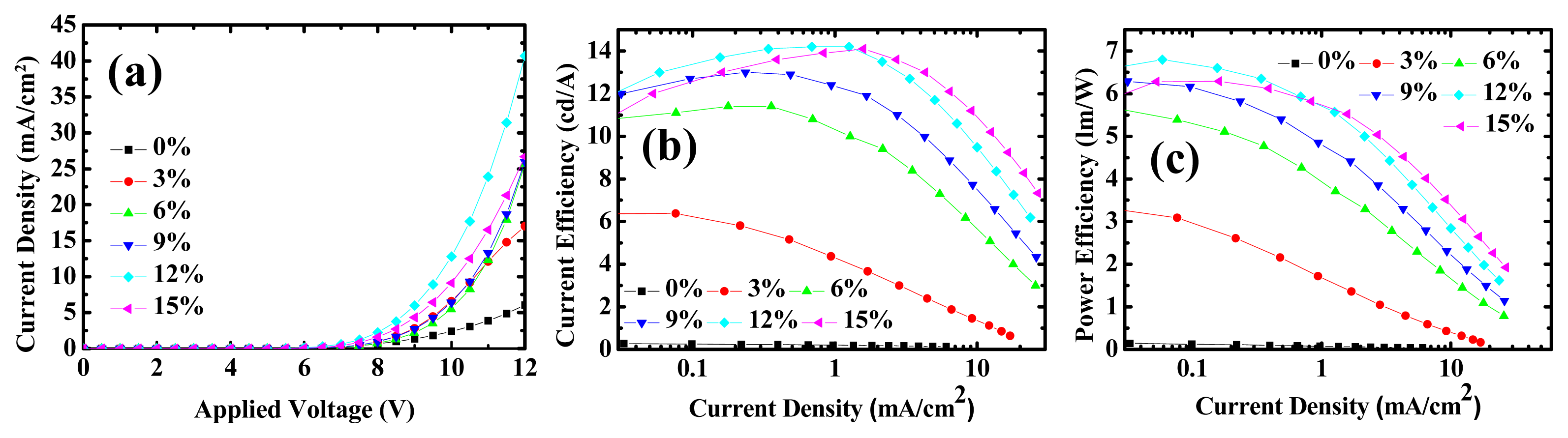
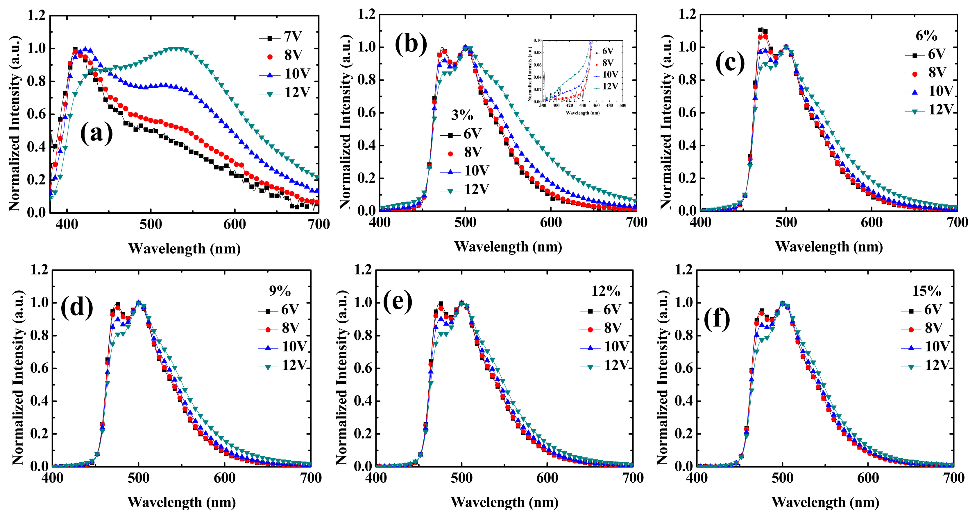
2.1. Device Performances of Blue Phosphorescent OLEDs with Different Dopant Concentrations

Figure 2a shows the J-V characteristics of OLEDs with different dopant concentrations. Compared to the non-doped case (device 1), doping FIrpic (devices 2–6) in the EML helps to reduce the driving voltage, as shown in Table II. Driving voltage is lowest for device 5. Figure 2b,c shows the current efficiency (in terms of cd/A) and power efficiency (in terms of lm/W), respectively. Device 5 also exhibits the highest maximum efficiency. Dopant material inside the matrix plays some role for better conduction, which may be: (1) better hole injection; (2) better hole transport; (3) better electron injection; (4) better electron transport; and (5) higher recombination current. In the following discussion, we will see that better electron injection is the main reason for the voltage reduction, and better electron transport shows only a minor effect.
Figure 3 shows the EL spectra for the six devices. For the case of undoped EML (device 1 in Figure 3a), a clear peak at 410 nm originates from mCP emission at lower driving voltage (7 and 8 V). On increasing the driving voltage to 10 and 12 V, this peak redshifts to 420 nm and disappears. On the other hand, the broad exciplex emission due to mCP/OXD interface around 530 nm increases monotonically with increasing driving voltage, which also implies that the recombination zone shifts from inside the OXD to the interface of mCP/OXD. At low driving voltage, the location of the recombination zone inside the OXD can be anticipated because this OXD exhibits certain hole-transporting characteristics. Besides, one can also see an increase around 430 nm with higher driving voltage, which comes from NPB emission, due to the recombination zone shift with increasing driving voltage. The multiple peak spectra in Figure 3a also implies that the recombination zone inside this device is quite broad, and covers NPB, mCP, and OXD. With increasing driving voltage, the recombination zone shifts toward the anode side. This means the electron mobility increases faster than the hole mobility with increasing driving voltage in the mCP and OXD layer. When the OXD is doped with 3% FIrpic (device 2 in Figure 3b), one can see the clear double peak emission at 474 and 502 nm from FIrpic emission, combined with some leakage at short wavelength (also shown in the inset of Figure 3b) and exciplex emission at long wavelength, which both increase with increasing driving voltage. For the double emission peak of Firpic, one can also see a relative decrease at the shorter wavelength (474 nm) with increasing driving voltage, which comes from the interference effect due to the recombination shift toward the anode side. This also implies that the recombination zone takes place inside the OXD layer at lower driving voltage (6 V) and shifts toward the anode side with increasing driving voltage. When the dopant concentration further increases (6%–15% in devices 3 to 6, as shown in Figure 3c–f), the main recombination takes place in the highly efficient FIrpic dopants. Relative increase of longer wavelength peaks of Firpic emission with increasing driving voltages are observed for all the devices, which means the recombination zone shifts from inside the OXD toward the anode side. Besides, when comparing the EL spectra at low driving voltages (6 V) with different dopant concentrations (3%–15%), the relative intensity at shorter wavelength increases from 3% to 6%, and then decreases from 6 to 15%. Not only increasing electron injection capability, FIrpic also plays some role in hole injection and transport. Under low concentration (3%–6%), holes inject through the FIrpic molecules which results in a blueshift. With further increasing FIrpic concentrations, the redshift comes from better electron injection and transport, together with the retardation of the holes. Comparing the J-V curves in Figure 2a, the driving voltage is lowest for device 5 (12%), due to the better electron injection and transport. However, when further increasing the dopant concentration to 15%, an increase in driving voltage is observed which comes from the hole-trapping effect of FIrpic on the OXD matrix.
Figure 4a shows the NPB emission at short wavelength (~430 nm) at 12 V for devices 2–6. One can see that the leakage decreases with increasing FIrpic concentration due to the increase of the recombination center. Figure 4b shows the photoluminescence (PL) spectra of OXD thin films doped with different concentrations (0%–15%). With increasing dopant concentration, emission from the OXD decreases which is transferred to the FIrpic emission. Besides, the emission spectra from FIrpic are always kept the same because the whole film is lit up with very little optical interference effect under optical pumping.

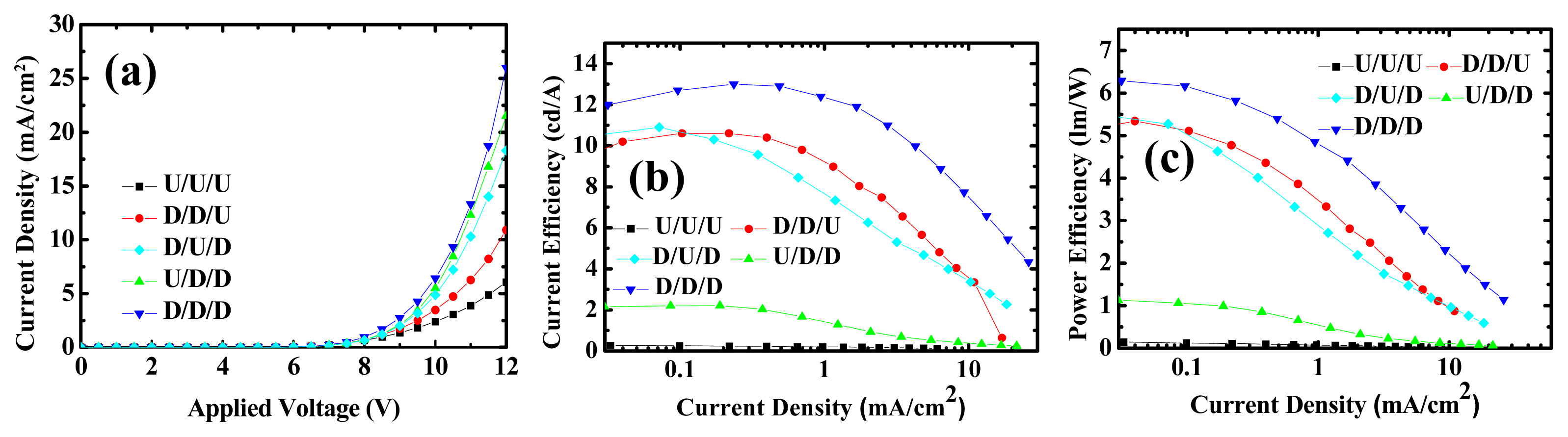
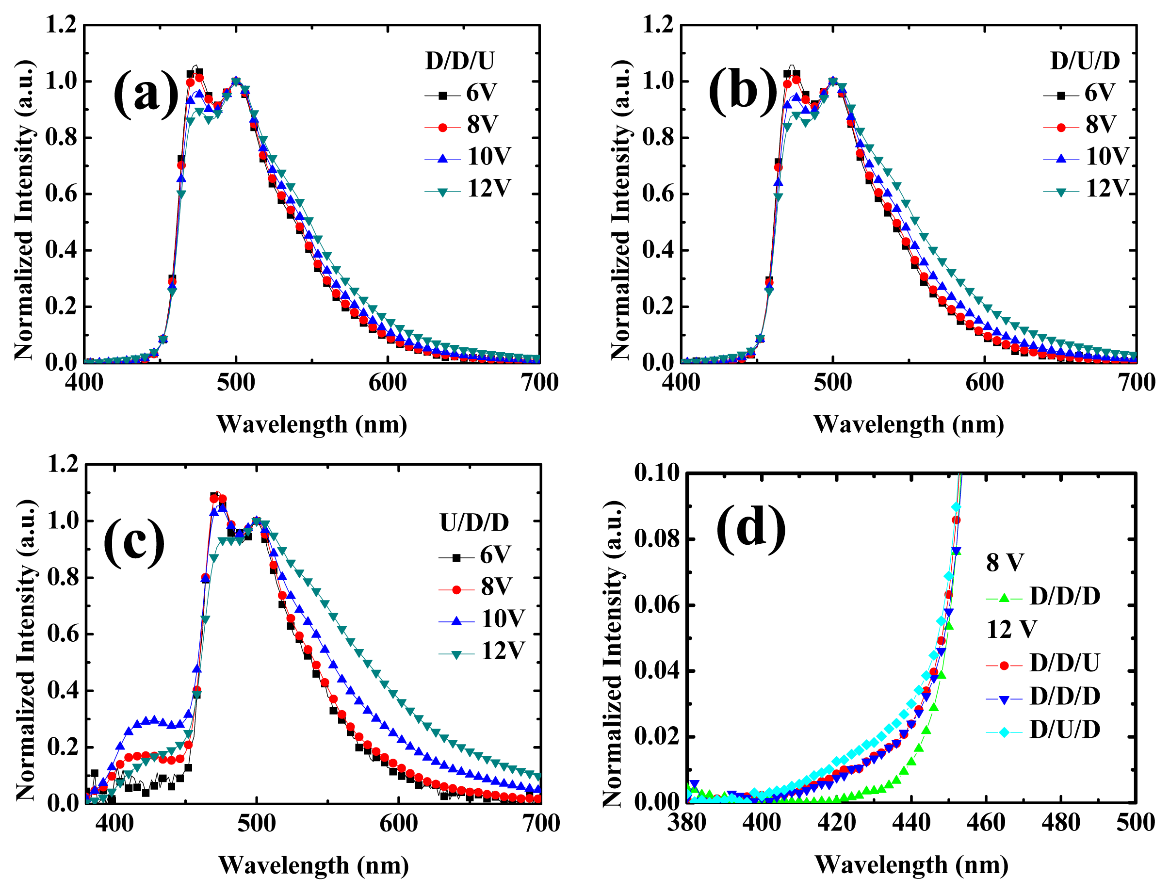
2.2. Device Performances of Blue Phosphorescent OLEDs with Different Doping Positions

To further analyze the effects of FIrpic molecules on electrical and optical characteristics of OLEDs, we doped 9% FIrpic at different positions of the EML. As shown in Table 1, there is an intentionally undoped region next to ETL, at the center, and next to EBL for devices 7, 8, and 9, respectively. Figure 5a shows the J-V characteristics of devices 1, 4, 7, 8, and 9. J-V curves of selective doped OLED (devices 7, 8, and 9) are all within the range between undoped (device 1) and uniform-doped (device 4), because the dopants assist voltage reduction. For the OLED with the undoped region close to ETL (device 7), the driving voltage is significant higher, which means the FIrpic dopant plays an important role in facilitating electron injection. Comparing device 8 and device 4, a small voltage increase indicates better electron transport characteristics in the FIrpic doped OXD layer. As shown in Table 2, for device 9 with the undoped region close to EBL, the driving voltage (9.88 V) is quite close to that of the uniformly doped one (9.67 V). When the undoped layer is close to EBL (device 9), the hole trap (FIrpic) is removed which improves hole mobility. On the other hand, the electron mobility decreases. These two effects compete which results in the driving voltage of device 9 (9.88 V) being quite close to that of the uniformly doped one (9.67 V in device 4). It also implies that the voltage reduction phenomenon with incorporation of FIrpic into OXD does not result from the increase of the recombination current. Figure 5b shows the curves of current efficiency under different current density. When the undoped region is close to the EBL (device 9), the maximum efficiency decreases to 2.21 cd/A. This value is low because the main recombination locates near the interface of the EBL/EML. However, this value is not very low which means the recombination zone is broad and extends inside EML towards the ETL at least 10 nm, which explains that when the undoped region is at the middle and close to the ETL, the maximum efficiency is ~10 cd/A, which is still lower than that of device 4 (13 cd/A).
Figure 6a–c shows the EL spectra under different driving voltages of devices 7, 8 and 9, respectively. Figure 6a,b are nearly identical except the exciplex hump around 550 nm is larger for the case of device 8, when the undoped region is at the middle of the EML. Because FIrpic dopants act as the recombination center, when there is no dopant at the middle of the EML, more electrons may transport to the interface of the EBL/EML interface for exciplex emission. Figure 6d shows the leakage emissions from device 4, 7 and 8, respectively. NPB leakage is nearly identical for devices 4 and 7 respectively, because the whole recombination zone (20 nm close to the EBL) is doped with FIrpic. On the other hand, NPB leakage is slightly higher for the case of device 8 with undoped region at the middle of the EML. Some electrons penetrate into the HTL for emission. For the EL spectra of device 9 with the undoped region close to the EBL interface, the spectra peak at shorter wavelength (474 nm) is higher than that in device 7 and 8, because the recombination zone locates far away from the EBL/EML interface (at least 10 nm) which blue-shifts the spectrum. Observing the light leakage at short wavelength, one can see the NPB emission increases from 6, 8, and 10 V, then decreases at 12 V. This implies the electron penetrates inside the NPB, and may further transport into the anode without recombination. After all, NPB is also a good electron transporter. Hence, here we may deduce that FIrpic inside the OXD serves as a recombination center to confine carrier not penetrating into the EBL, as well as HTL.

3. Experimental Section

Our devices were fabricated on the patterned indium-tin-oxide (ITO) substrate with pixel size of 2 mm × 2 mm. After O2 plasma treatment, the device is transferred to the multisource evaporator for organic layer and cathode deposition under ultra high vacuum 5 × 10⁻⁶ torr. Then, it is transferred to the glovebox for the encapsulation process. Electrical and optical characteristics are determined with a source meter (Keithley 2400) and spectroradiometer (Minolta CS-1000), respectively. Photoluminescence (PL) of organic thin films is carried out by Hitachi F-4500.

4. Conclusions

In summary, by analyzing the J-V characteristics, efficiency, and EL spectra of OLEDs with different concentration and dopant profile of FIrpic in the OLED, we can conclude that: (1) FIrpic aids electron injection from ETL into EML; (2) it also helps electron transport; (3) on the other hand, under low dopant concentrations (3%–6%), it may also assist hole injection; (4) additionally, it is a hole trap which retards hole transport.

Acknowledgments

This work was supported by the National Science Council, R.O.C., under Grant NSC 99-2218-E-155-003, NSC 99-2221-E-155-092, NSC 99-2622-E-155-010-CC3, 100-2622-E-155-008-CC3 and 100-2221-E-155-046.

References

  1. Tang, C.W.; VanSlyke, S.A. Organic electroluminescent diodes. Appl. Phys. Lett 1987, 51, 913–915. [Google Scholar]
  2. Zhang, B.; Tan, G.; Lam, C.S.; Yao, B.; Ho, C.L.; Liu, L.; Xie, Z.; Wong, W.Y.; Ding, J.; Wang, L. High-efficiency single emissive layer white organic light-emitting diodes based on solution-processed dendritic host and new orange-emitting Iridium complex. Adv. Mater 2012, 24, 1873–1877. [Google Scholar]
  3. Zhou, G.; Wang, Q.; Ho, C.L.; Wong, W.Y.; Ma, D.; Wang, L. Duplicating “sunlight” from simple WOLEDs for lighting applications. Chem. Commun 2009, 3574–3576. [Google Scholar]
  4. Zhou, G.; Wong, W.Y.; Suo, S. Recent progress and current challenges in phosphorescent white organic light-emitting diodes (WOLEDs). J. Photochem. Photobiol. C Photochem. Rev 2010, 11, 133–156. [Google Scholar]
  5. Wu, H.; Zhou, G.J.; Zou, J.; Ho, C.L.; Wong, W.Y.; Yang, W.; Peng, J.; Cao, Y. Efficient polymer white-light-emitting devices for solid-state lighting. Adv. Mater 2009, 21, 4181–4184. [Google Scholar]
  6. Reineke, S.; Lindner, F.; Schwartz, G.; Seidler, N.; Walzer, K.; Lüssem, B.; Leo, K. White organic light-emitting diodes with fluorescent tube efficiency. Nature 2009, 459, 234–238. [Google Scholar]
  7. Zheng, T.; Choy, W.C.H. High efficiency blue organic LEDs achieved by an integrated fluorescence–interlayer–phosphorescence emission architecture. Adv. Funct. Mater 2010, 20, 648–655. [Google Scholar]
  8. Chou, H.H.; Cheng, C.H. A highly efficient universal bipolar host for blue, green, and red phosphorescent OLEDs. Adv. Mater 2010, 22, 2468–2471. [Google Scholar]
  9. Fan, C.; Chen, Y.; Jiang, Z.; Yang, C.; Zhong, C.; Qin, J.; Ma, D. Diarylmethylene-bridged triphenylamine derivatives encapsulated with fluorene: Very high Tg host materials for efficient blue and green phosphorescent OLEDs. J. Mater. Chem 2010, 20, 3232–3237. [Google Scholar]
  10. Jang, S.E.; Joo, C.W.; Jeon, S.O.; Yook, K.S.; Lee, J.Y. The relationship between the substitution position of the diphenylphosphine oxide on the spirobifluorene and device performances of blue phosphorescent organic light-emitting diodes. Org. Electron 2010, 11, 1059–1065. [Google Scholar]
  11. Lee, J.; Lee, J.I.; Chu, H.Y. Improved performance of white phosphorescent organic light-emitting diodes through a mixed-host structure. ETRI J 2009, 31, 642–646. [Google Scholar]
  12. Kappaun, S.; Slugovc, C.; List, E.J.W. Phosphorescent organic light-emitting devices: Working principle and iridium based emitter materials. Int. J. Mol. Sci 2008, 9, 1527–1547. [Google Scholar]
  13. Cheng, G.; Zhang, Y.; Zhao, Y.; Lin, Y.; Ruan, C.; Liu, S.; Fei, T.; Ma, Y.; Cheng, Y. White organic light-emitting devices with a phosphorescent multiple emissive layer. Appl. Phys. Lett 2006, 89, 043504:1–043504:3. [Google Scholar]
  14. Zhou, G.; Wong, W.Y.; Yang, X. New design tactics in OLEDs using functionalized 2-phenylpyridine-type cyclometalates of Iridium(III) and Platinum(II). Chem. Asian J 2011, 6, 1706–1727. [Google Scholar]
  15. Wong, W.Y.; Ho, C.L. Heavy metal organometallic electrophosphors derived from multi-component chromophores. Coord. Chem. Rev 2009, 253, 1709–1758. [Google Scholar]
  16. Lee, J.H.; Ho, Y.H.; Lin, T.C.; Wu, C.F. High-efficiency fluorescent blue organic light-emitting device with balanced carrier transport. J. Electrochem. Soc 2007, 154, J226–J228. [Google Scholar]
  17. Lee, J.H.; Huang, C.L.; Hsiao, C.H.; Leung, M.K.; Yang, C.C.; Chao, C.C. Blue phosphorescent organic light-emitting device with double emitting layer. Appl. Phys. Lett 2009, 94, 223301:1–223301:3. [Google Scholar]
  18. Lan, Y.H.; Hsiao, C.H.; Lee, P.Y.; Bai, Y.C.; Lee, C.C.; Yang, C.C.; Leung, M.K.; Wei, M.K.; Chiu, T.L.; Lee, J.H. Dopant effects in phosphorescent white organic light-emitting device with double-emitting layer. Org. Electron 2011, 12, 756–765. [Google Scholar]
  19. Zou, J.; Wu, H.; Lam, C.S.; Wang, C.; Zhu, J.; Zhong, C.; Hu, S.; Ho, C.L.; Zhou, G.J.; Wu, H.; et al. Simultaneous optimization of charge-carrier balance and luminous efficacy in highly efficient white polymer light-emitting devices. Adv. Mater 2011, 23, 2976–7980. [Google Scholar]
  20. Wong, W.Y.; Ho, C.L. Functional metallophosphors for effective charge carrier injection/transport: New robust OLED materials with emerging applications. J. Mater. Chem 2009, 19, 4457–4482. [Google Scholar]
  21. Choi, W.H.; Cheung, C.H.; So, S.K. Can an organic phosphorescent dye act as a charge transporter? Org. Electron 2010, 11, 872–875. [Google Scholar]
  22. Adachi, C.; Kwong, R.; Forrest, S.R. Efficient electrophosphorescence using a doped ambipolar conductive molecular organic thin film. Org. Electron 2001, 2, 37–43. [Google Scholar]
  23. Matsusue, N.; Ikame, S.; Suzuki, Y.; Naito, H. Charge-carrier transport and triplet exciton diffusion in a blue electrophosphorescent emitting layer. J. Appl. Phys 2005, 97, 123512:1–123512:5. [Google Scholar]
  24. Matsusue, N.; Ikame, S.; Suzuki, Y.; Naito, H. Charge carrier transport in an emissive layer of green electrophosphorescent devices. Appl. Phys. Lett 2004, 85, 4046–4048. [Google Scholar]
  25. Noh, S.; Suman, C.K.; Hong, Y.; Lee, C. Carrier conduction mechanism for phosphorescent material doped organic semiconductor. J. Appl. Phys 2009, 105, 033709:1–033709:5. [Google Scholar]
  26. Chiu, T.L.; Lee, J.H.; Hsiao, Y.P.; Lin, C.F.; Chao, C.C.; Leung, M.K.; Wan, D.H.; Chen, H.L.; Ho, H.C. Absorptive and conductive cavity cathode with silver nanoparticles for low reflection organic light-emitted devices. J. Phys. D Appl. Phys 2011, 44, 095102:1–095102:6. [Google Scholar]
  27. Chiu, T.L.; Xu, W.F.; Lin, C.F.; Lee, J.H.; Chao, C.C.; Leung, M.K. Optical and electrical characteristics of Ag-doped perylene diimide derivative. Appl. Phys. Lett 2009, 94, 13307:1–13307:3. [Google Scholar]
  28. Li, X.C.; Yong, T.M.; Grüner, J.; Holmes, A.B.; Moratti, S.C.; Cacialli, F.; Friend, R.H. A blue light emitting copolymer with charge transporting and photo-crosslinkable functional units. Synth. Met 1997, 84, 437–438. [Google Scholar]
  29. Li, X.C.; Kraft, A.; Cervini, R.; Spencer, G.C.W.; Cacialli, F.; Friend, R.H.; Grüner, J.; Holmes, A.B.; DeMello, J.C.; Moratti, S.C. Synthesis and optoelectronic properties of oxadiazole-based polymers. Mater. Res. Soc. Symp. Proc 1996, 413, 13–22. [Google Scholar]
  30. He, Z.; Wong, W.Y.; Yu, X.; Kwok, H.S.; Lin, Z. Phosphorescent Platinum(II) complexes derived from multifunctional chromophores: Synthesis, structures, photophysics, and electroluminescence. Inorg. Chem 2006, 45, 10922–10937. [Google Scholar]
  31. Wong, W.Y.; He, Z.; So, S.K.; Tong, K.L.; Lin, Z. A multifunctional platinum-based triplet emitter for OLED applications. Organometallics 2005, 24, 4079–4082. [Google Scholar]
  32. Chiu, T.L.; Lee, P.Y.; Lee, J.H.; Hsiao, C.H.; Leung, M.K.; Lee, C.C.; Chen, C.Y.; Yang, C.C. Oxadiazole host for a phosphorescent organic light-emitting device. J. Appl. Phys 2011, 109, 084520:1–084520:17. [Google Scholar]
  33. Yu, X.M.; Zhou, G.J.; Lam, C.S.; Wong, W.Y.; Zhu, X.L.; Sun, J.X.; Wong, M.; Kwok, H.S. A yellow-emitting iridium complex for use in phosphorescent multiple-emissive-layer white organic light-emitting diodes with high color quality and efficiency. J. Organomet. Chem 2008, 693, 1518–1527. [Google Scholar]
  34. Yu, X.M.; Kwok, H.S.; Wong, W.Y.; Zhou, G.J. High-efficiency white organic light-emitting devices based on a highly amorphous Iridium(III) orange phosphor. Chem. Mater 2006, 18, 5097–5103. [Google Scholar]
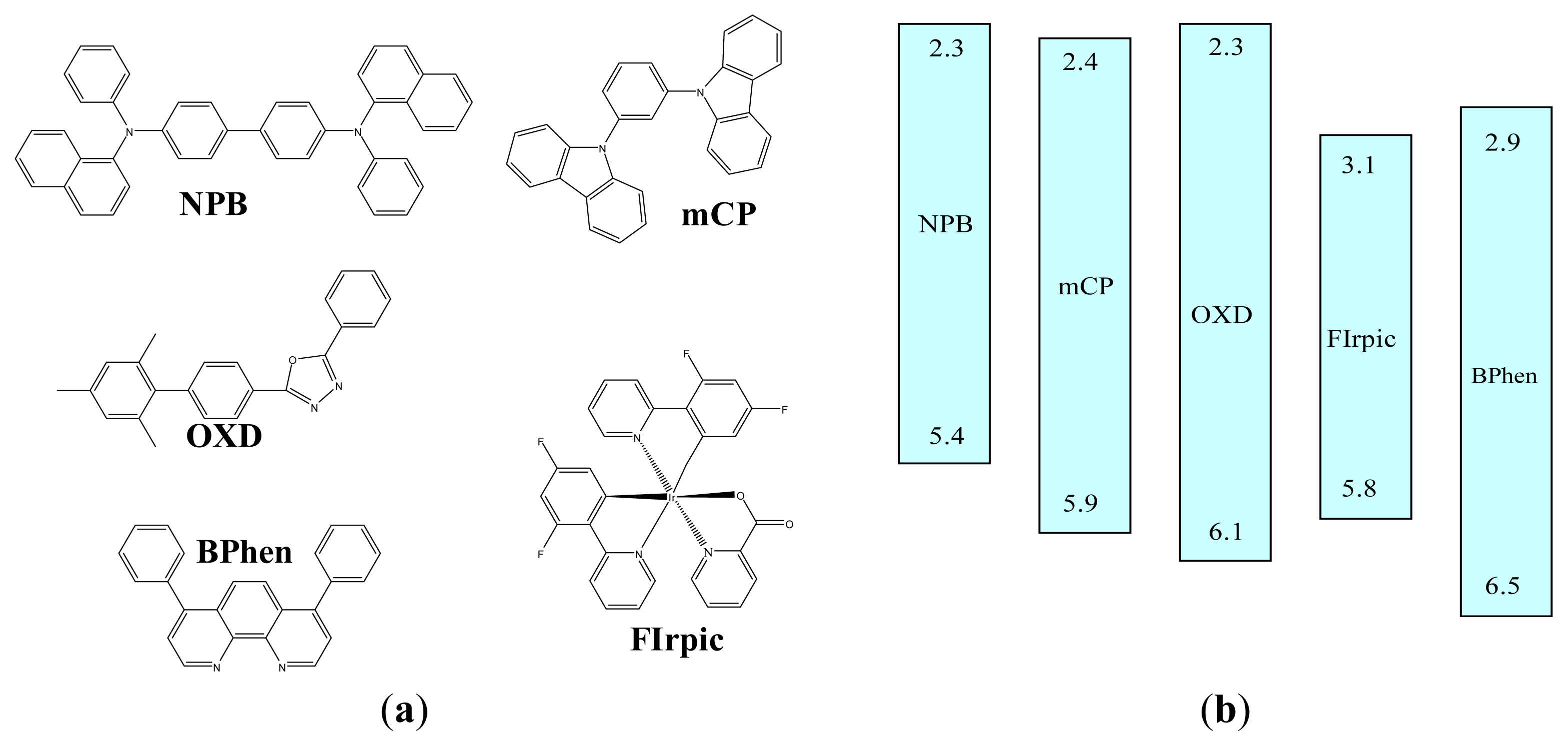
Figure 1. (a) Molecular structures of NPB, mCP, OXD, FIrpic, and BPhen; (b) Energy levels of all used organic materials.
Ijms 13 07575f1
Figure 2. Comparison of (a) current density versus voltage; (b) current efficiency (cd/A) versus current density; and (c) power efficiency (lm/W) versus current density for devices 1 to 6.
Ijms 13 07575f2
Figure 3. Electroluminescence (EL) spectra at different voltages of devices 1–6 ((af), respectively).
Ijms 13 07575f3
Figure 4. (a) Zoom-in of EL spectra of devices 1–6 at high voltages (12 V); (b) photoluminescence (PL) spectra of OXD thin film (100 nm) doped with different FIrpic concentrations (0%–15%).
Ijms 13 07575f4
Figure 5. Comparison of (a) current density versus voltage; (b) current efficiency (cd/A) versus current density; and (c) power efficiency (lm/W) versus current density for devices 1, 4, 7, 8, and 9.
Ijms 13 07575f5
Figure 6. EL Spectra at different voltages of devices (a) 7, (b) 8, and (c) 9. (d) Zoom-in of EL spectra of devices 4, 7, and 8.
Ijms 13 07575f6
Table 1. Layer structures of organic light-emitting devices (OLEDs).
DeviceHTLEBLEML (30 nm)ETLEILCathode

NPBmCPFIrpic in OXDBPhenLiFAl

10%
23%
36%
49%
512%
650 nm10 nm15%40 nm1.2 nm100 nm

DeviceEML1 (10 nm)EML2 (10 nm)EML3 (10 nm)

79%9%0%
89%0%9%
90%9%9%
Table 2. Electrical and optical properties of the OLEDs.
DeviceVolt. @5 mA/cm2Max. lm/WMax. cd/A
111.60.17 @ 5.5 V0.77 @ 5 V
29.633.33 @ 6 V6.38 @ 6.5 V
39.875.65 @ 6 V11.4 @ 6.5 V
49.676.29 @ 6 V13 @ 6.5 V
58.786.80 @ 6 V14.2 @ 7 V
69.166.29 @ 6 V14.1 @ 7.5 V
710.65.34 @ 6 V10.6 @ 6.5 V
8105.47 @ 6 V10.9 @ 6.5 V
99.881.13 @ 6 V2.21 @ 7 V

