Structural and Optical Properties of Nanoscale Galinobisuitite Thin Films


Abstract
:1. Introduction
2. Results and Discussion
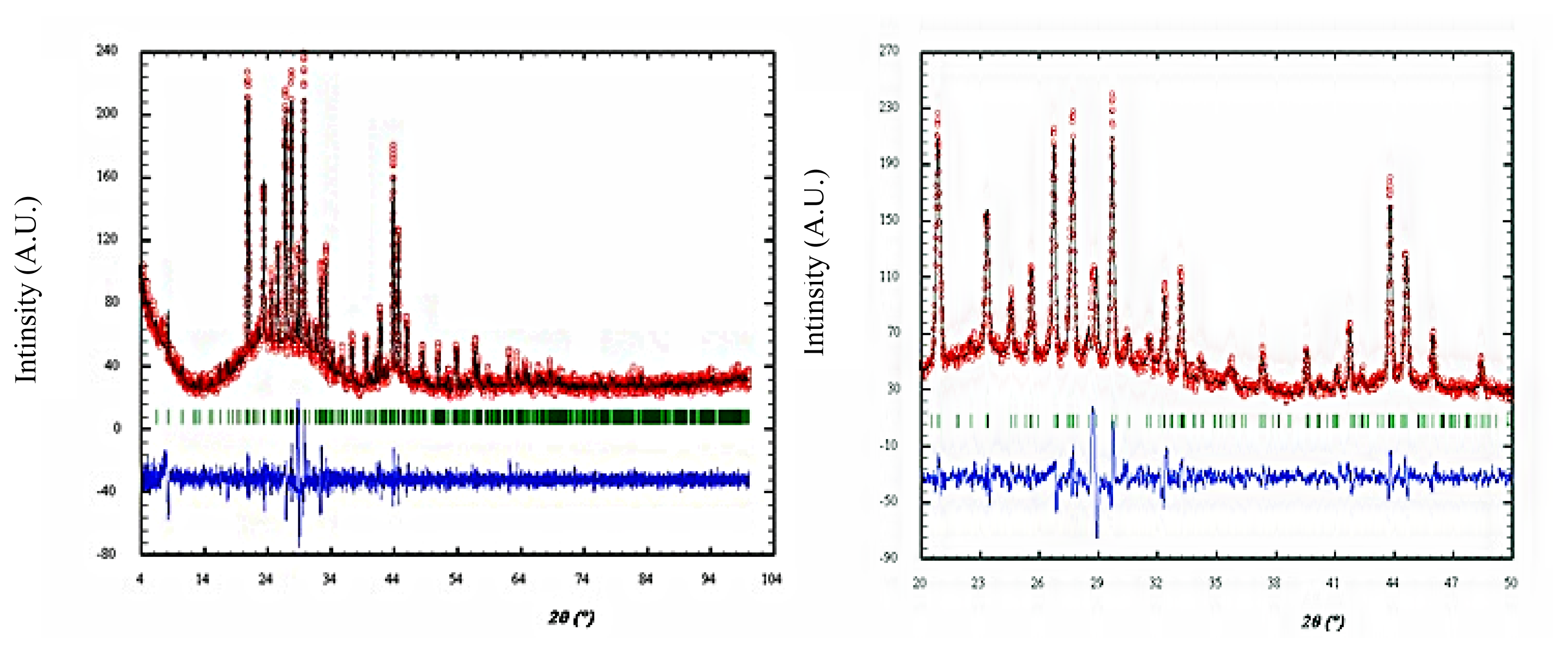
2.1. Structural Analysis
2.1.1. Crystal Structure of Bi2S3
2.1.2. Crystal Structure of PbS
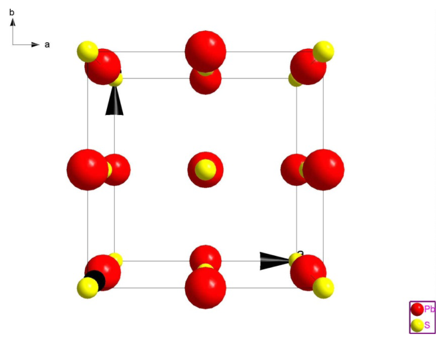
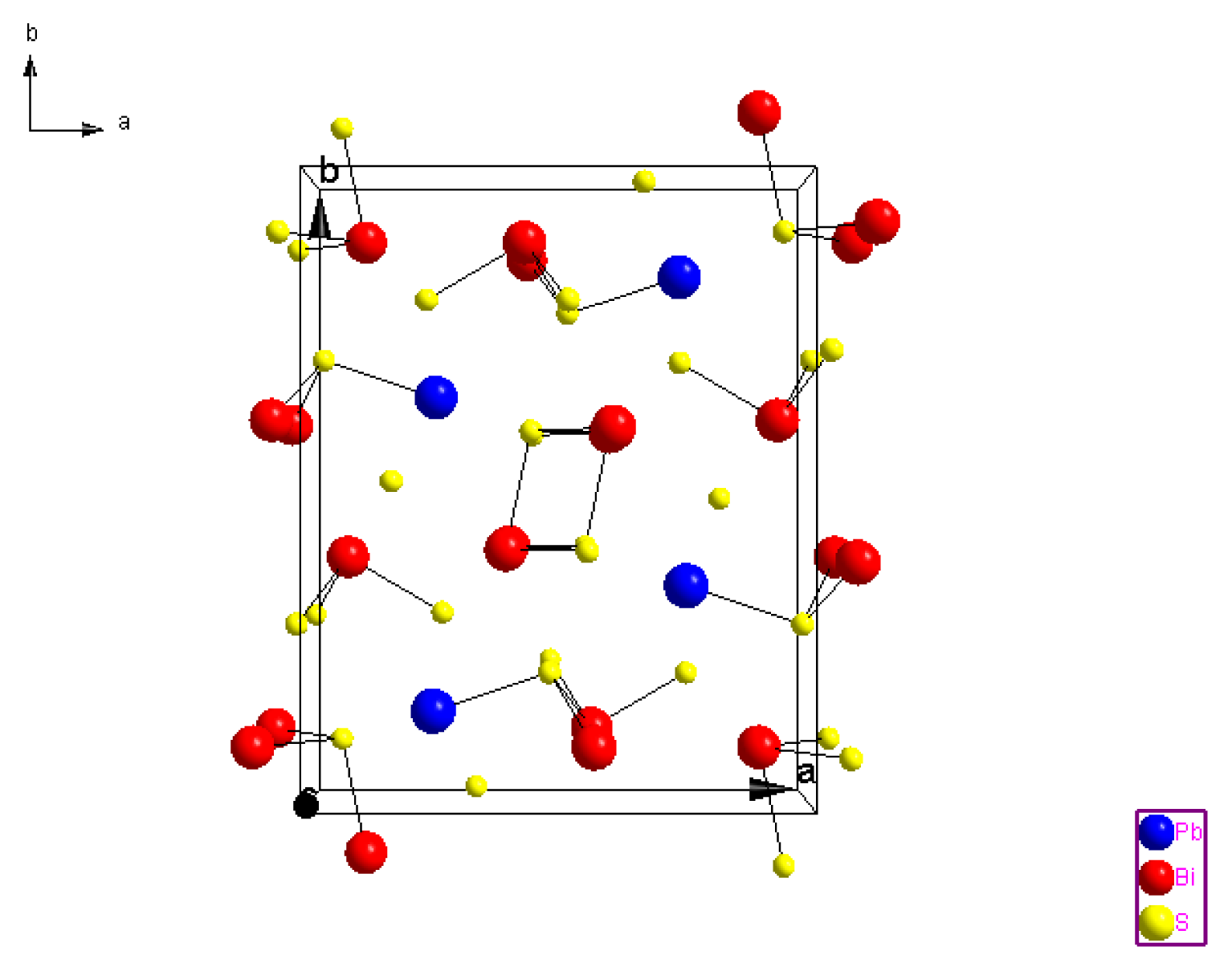
2.1.3. Crystal Structure of Galenobismutite (PbS)(Bi2S3)
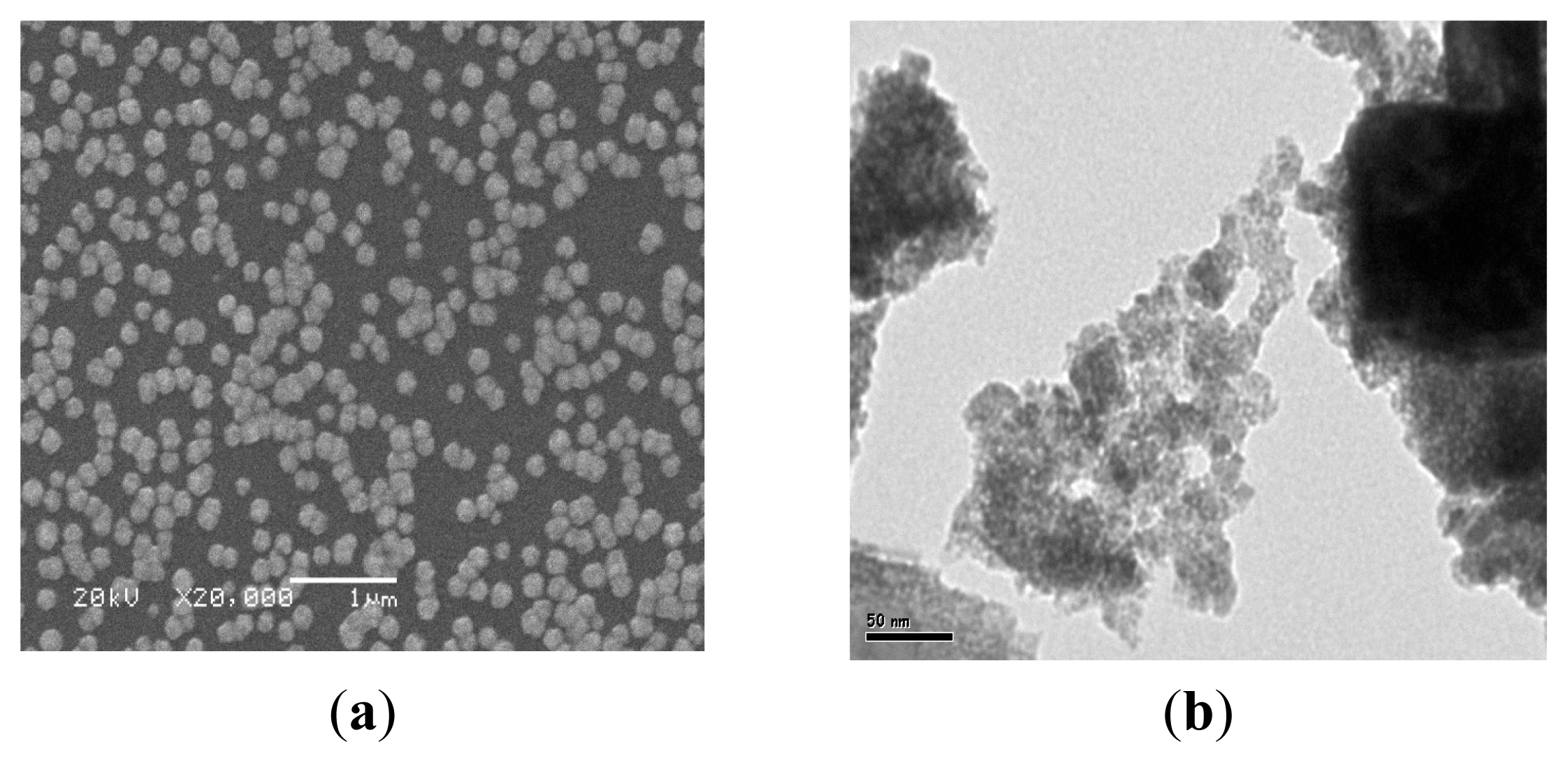
2.2. The Surface Morphology Studies
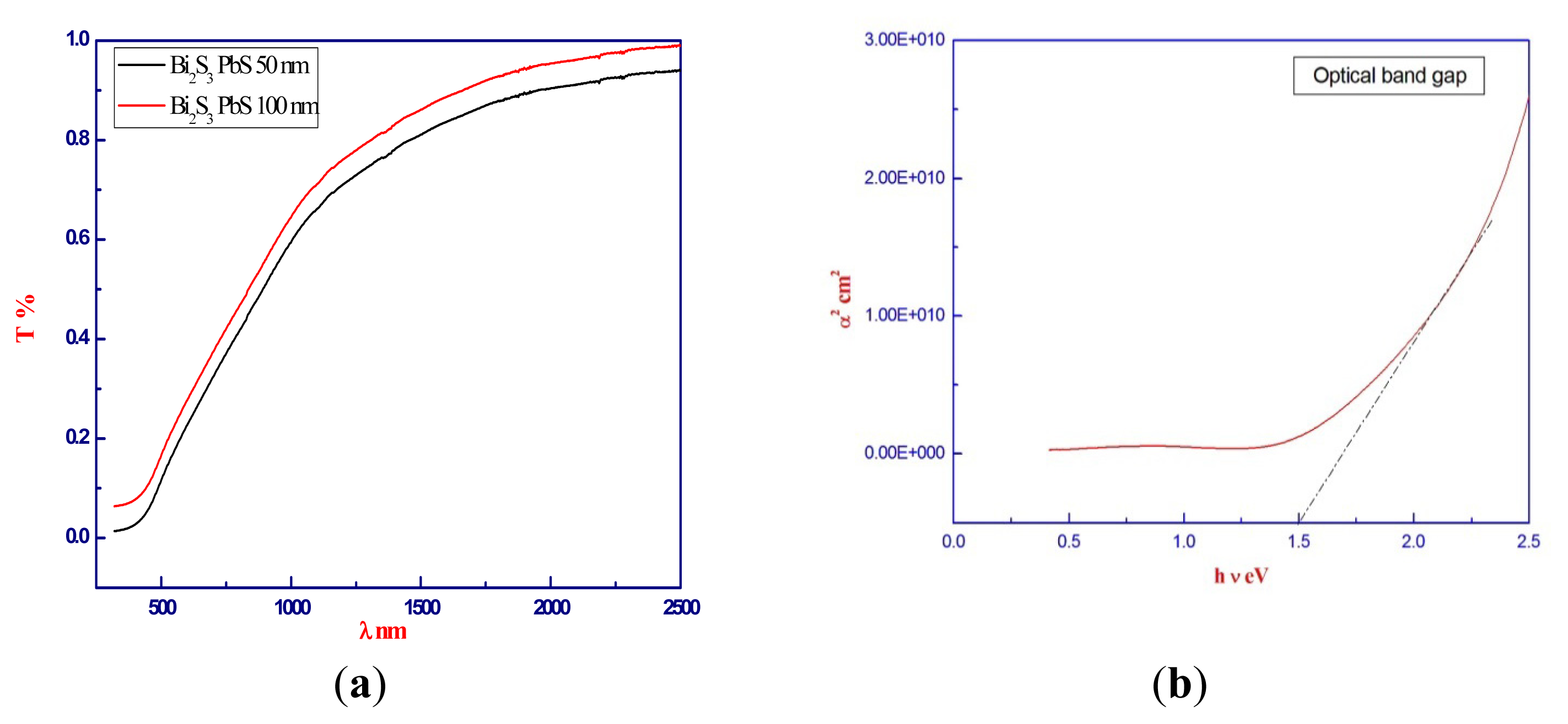
2.3. The Optical Properties Studies
3. Experimental Section
3.1. Experimental Procedure
3.2. Measurment of Atomic Absorption
4. Conclusions
Acknowledgments
Conflicts of Interest
References
- Mahmoud, S.; Eid, A.H.; Omar, H. Optical characteristics of bismuth sulfide (Bi2S3) thin films. Fizika A 1997, 3, 111–120. [Google Scholar]
- Mahmoud, S.; Omar, H. Growth and characterization of lead-sulfide films deposited on glass substrates. Fizika A 2001, 1, 21–30. [Google Scholar]
- Ajji, Z. Grafting of poly(vinyl pyrrolidone) with citric acid using gamma irradiation. Nuclear Instrum. Methods Phys. Res. B 2007, 265, 179–182. [Google Scholar]
- Wang, C.; Shen, E.; Wang, E.; Gao, L. Controllable synthesis of ZnO nanocrystals via a surfactant-assisted alcohol thermal process at a low temperature. Mater. Lett 2005, 59, 2867–2871. [Google Scholar]
- Malika, B.; Noureddine, B.; Mourad, M.; Abdelkader, O.; Attouya, B.; Hind, T.-D. Investigations in structural morphological and optical properties of Bi–Pb–S system thin films. Results Phys 2013, 3, 30–37. [Google Scholar]
- Abd Elkader, O. Preparation and characterization of nanostructured zinc oxide thin films. Proceedings of International Conference on Fundamental and Applied Sciences (ICFAS 2012), Kuala Lumpur, Malaysia, 12–14 June 2012.
- Kupcik, V.; Vesla-Novakova, L. Zur Kristallstruktur des. Bismuthinits Bi2S3. Tschermaks Miner. U. Petrogr. Mitt 1970, 14, 55–59. [Google Scholar]
- Berry, L.G. Studies of mineral sulpho-salts: IV galenobismutite and lillianite. Amer. Min 1940, 25, 726–734. [Google Scholar]
- Yamazaki, T.; Watakabe, Y.; Suzuki, Y.; Nakata, H. A dry etching technique using electronn beam resist-PbS. J. Electrochem. Soc 127.
- Noda, Y.; Ohba, S.; Sato, S.; Saito, Y. Charge distribution and atomic thermal vibration in lead chalcogenide crystals. Acta Crystal. Sect. B 1983, 39, 312–317. [Google Scholar]
- Wickman, F.E. Galenobismutite PbBi2S4. cf. Ag-free lillianite, structure. Ark. Min 1951, 1, 219. [Google Scholar]
- Iitaka, Y.; Nowacki, W. A Redetermination of the crystal structure of galenobismutite, PbBi2S4. Acta Crystallogr 1962, 15, 691–698. [Google Scholar]
- Said, M.S.; Zemel, N.J. Properties of PbS-PbO crystalline films. I. Preparation and physical Structure. J. Appl. Phys 1976, 47, 886–870. [Google Scholar]
- Isomura, S.; Shirakata, S.; Abe, T. Some properties of CuInSe2 films prepared by vacuum evaporation of elements. Solar Energy Mater 1991, 22, 223. [Google Scholar]
- Susama, M.; Padhi, H.C. Preparation and characterization of (Bi2S3)1−x(CdS)x solid solution thin films. J. Appl. Phys 1994, 75, 4576–4580. [Google Scholar]
- Mahmoud, S.; Omar, H. Structure and optical properties of thermally deposited bismuth sulfide-lead sulfide films. J. Appl. Sci. Res 2008, 4, 303–310. [Google Scholar]
- Nieseni, P.T.; de Guire, R.M. Review: Deposition of ceramic thin films at low temperatures from aqueous solutions. J. Electroceram 2001, 6, 169–207. [Google Scholar]
- APHA-AWWA-WPCF, Standard Methods for the Examination of Water and Wastewater, 17th ed.; American Public Health Association: Washington, DC, USA, 1989.


| Cell constant (Å) | Berry (1940) | Wickman (1951) | Itaka (1962) |
|---|---|---|---|
| a | 11.72 (3) | 11.65 (5) | 11.79 (7) |
| b | 14.52 (3) | 14.49 (3) | 14.59 (8) |
| c | 4.07 (2) | 4.08 (3) | 4.10 (5) |
| Space group | (Pnam) | (Pna2) | (Pnam) |
| Axis | X | Y | Z |
|---|---|---|---|
| Pb | 0.24792 (15) | 0.65126 (10) | 0.25000 |
| Bi (I) | 0.06750 (14) | 0.39009 (10) | 0.25000 |
| Bi (II) | 0.10427 (14) | 0.90559 (11) | 0.25000 |
| S (I) | 0.33072 (92) | 0.01411 (69) | 0.25000 |
| S (II) | 0.26091 (88) | 0.29968 (74) | 0.25000 |
| S (III) | 0.05499 (93) | 0.09269 (71) | 0.25000 |
| S (IV) | 0.01808 (97) | 0.7119 (70) | 0.25000 |
| a | b | c | α | β | γ | Volume | Space group |
|---|---|---|---|---|---|---|---|
| 10.785 | 13.954 | 8.488 | 90 | 90 | 90 | 1277.52 | P 222 |
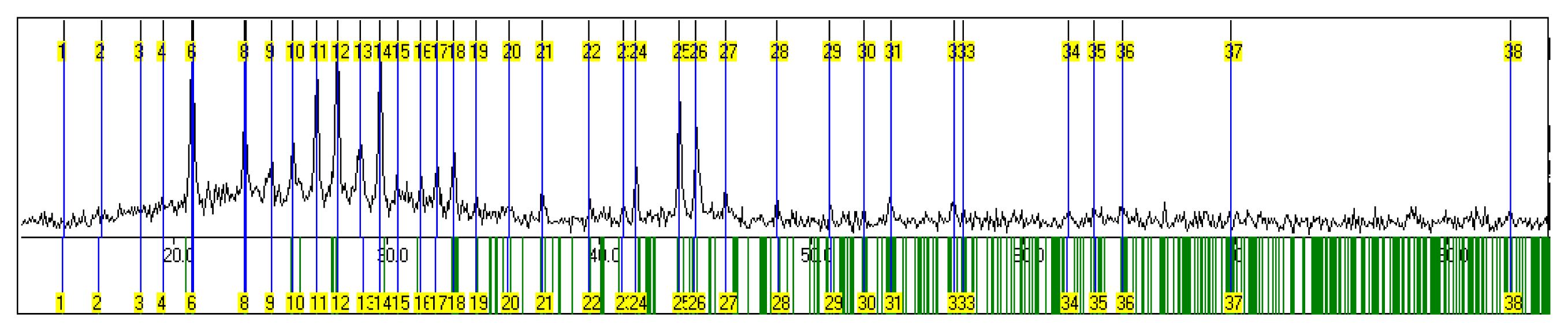
| No | h | k | l | 2Θ(Obs) | 2Θ(Calc) | Diff. | d-values |
|---|---|---|---|---|---|---|---|
| 1 | 1 | 1 | 1 | 14.820 | 14.720 | 0.100 | 5.9776 |
| 2 | 0 | 2 | 1 | 16.540 | 16.446 | 0.094 | 5.3596 |
| 3 | 1 | 2 | 1 | 18.400 | 18.402 | −0.002 | 4.8218 |
| 4 | 2 | 0 | 1 | 19.470 | 19.502 | −0.032 | 4.5592 |
| 5 | 2 | 2 | 0 | 20.816 | 20.819 | −0.003 | 4.2673 |
| 6 | 0 | 0 | 2 | 20.879 | 20.930 | −0.051 | 4.2546 |
| 7 | 1 | 3 | 1 | 23.311 | 23.315 | −0.004 | 3.8159 |
| 8 | 1 | 1 | 2 | 23.390 | 23.409 | −0.019 | 3.8032 |
| 9 | 0 | 2 | 2 | 24.571 | 24.550 | 0.021 | 3.6230 |
| 10 | 3 | 1 | 0 | 25.597 | 25.587 | 0.010 | 3.4801 |
| 11 | 2 | 0 | 2 | 26.715 | 26.729 | −0.014 | 3.3369 |
| 12 | 3 | 1 | 1 | 27.693 | 27.695 | −0.002 | 3.2213 |
| 13 | 1 | 4 | 1 | 28.758 | 28.882 | −0.124 | 3.1044 |
| 14 | 2 | 2 | 2 | 29.705 | 29.689 | 0.016 | 3.0075 |
| 15 | 2 | 4 | 0 | 30.527 | 30.520 | 0.007 | 2.9284 |
| 16 | 0 | 0 | 3 | 31.599 | 31.621 | −0.022 | 2.8314 |
| 17 | 2 | 4 | 1 | 32.342 | 32.333 | 0.009 | 2.7681 |
| 18 | 1 | 5 | 0 | 33.148 | 33.158 | −0.010 | 2.7026 |
| 19 | 0 | 2 | 3 | 34.204 | 34.196 | 0.008 | 2.6215 |
| 20 | 4 | 2 | 0 | 35.768 | 35.699 | 0.069 | 2.5104 |
| 21 | 2 | 4 | 2 | 37.310 | 37.300 | 0.010 | 2.4101 |
| 22 | 1 | 5 | 2 | 39.541 | 39.540 | 0.001 | 2.2791 |
| 23 | 3 | 1 | 3 | 41.176 | 41.109 | 0.067 | 2.1923 |
| 24 | 4 | 2 | 2 | 41.768 | 41.746 | 0.022 | 2.1630 |
| 25 | 5 | 1 | 1 | 43.788 | 43.785 | 0.003 | 2.0674 |
| 26 | 2 | 4 | 3 | 44.560 | 44.521 | 0.039 | 2.0334 |
| 27 | 2 | 0 | 4 | 45.973 | 45.958 | 0.015 | 1.9741 |
| 28 | 4 | 2 | 3 | 48.397 | 48.423 | −0.026 | 1.8808 |
| 29 | 5 | 4 | 1 | 50.895 | 50.922 | −0.027 | 1.7942 |
| 30 | 3 | 7 | 0 | 52.507 | 52.489 | 0.018 | 1.7428 |
| 31 | 6 | 2 | 1 | 53.735 | 53.756 | −0.021 | 1.7058 |
| 32 | 4 | 2 | 4 | 56.747 | 56.760 | −0.013 | 1.6222 |
| 33 | 1 | 7 | 3 | 57.162 | 57.167 | −0.005 | 1.6115 |
| 34 | 4 | 6 | 3 | 62.122 | 62.077 | 0.045 | 1.4942 |
| 35 | 2 | 9 | 1 | 63.367 | 63.374 | −0.007 | 1.4678 |
| 36 | 7 | 3 | 1 | 64.658 | 64.668 | −0.010 | 1.4416 |
| 37 | 8 | 0 | 0 | 69.760 | 69.755 | 0.005 | 1.3481 |
| 38 | 6 | 4 | 5 | 82.940 | 82.989 | −0.049 | 1.1641 |
© 2014 by the authors; licensee MDPI, Basel, Switzerland This article is an open access article distributed under the terms and conditions of the Creative Commons Attribution license (http://creativecommons.org/licenses/by/3.0/).
Share and Cite
Abd-Elkader, O.H.; Deraz, N.M. Structural and Optical Properties of Nanoscale Galinobisuitite Thin Films. Int. J. Mol. Sci. 2014, 15, 1842-1851. https://doi.org/10.3390/ijms15021842
Abd-Elkader OH, Deraz NM. Structural and Optical Properties of Nanoscale Galinobisuitite Thin Films. International Journal of Molecular Sciences. 2014; 15(2):1842-1851. https://doi.org/10.3390/ijms15021842
Chicago/Turabian StyleAbd-Elkader, Omar H., and N. M. Deraz. 2014. "Structural and Optical Properties of Nanoscale Galinobisuitite Thin Films" International Journal of Molecular Sciences 15, no. 2: 1842-1851. https://doi.org/10.3390/ijms15021842