In Situ Roughness Measurements for the Solar Cell Industry Using an Atomic Force Microscope

Abstract
:1. Introduction
2. Experimental
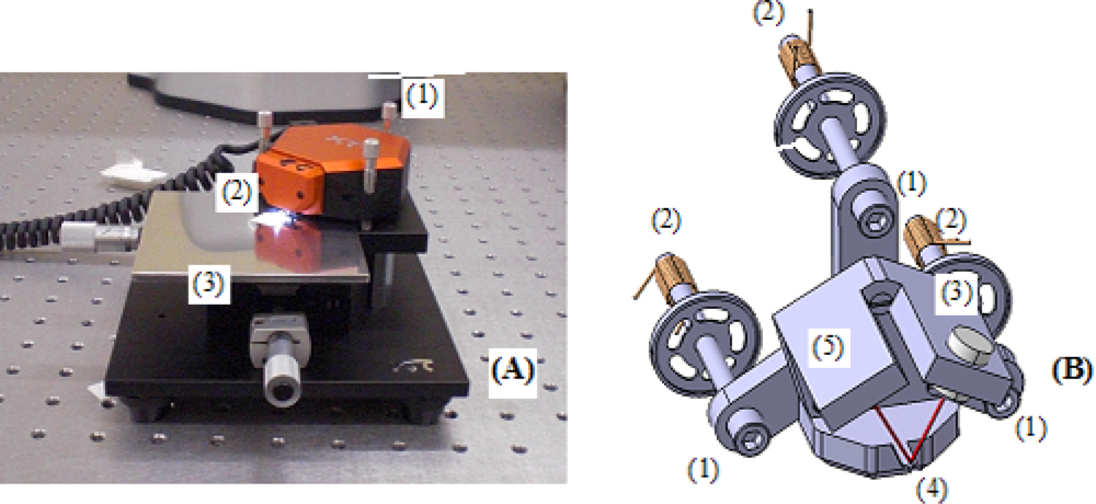
2.1. AFM Instrument
- - Operating mode: Tapping mode
- - Cantilever force: 20 nN
- - Image resolution: 256 points per line (ppl)
- - Lines: 256
- - Time per line: 1 s
- - Cantilever type: Nanosensors NCLR [15]
- - Vibration frequency: 159.4 kHz
- - Measurement time: 8 min 30 s (approximate)
2.2. Validation Process
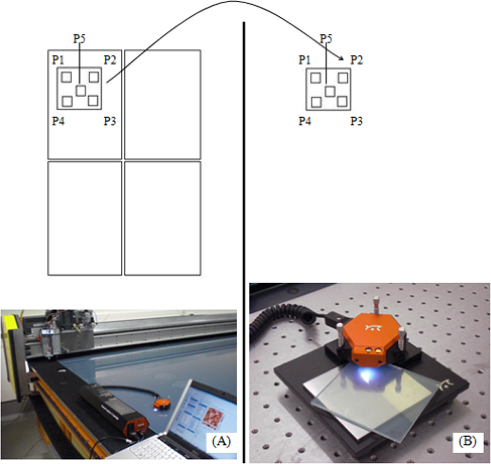
- - A region of interest (10 cm2) is selected on a large panel (5.4 m2) on the cutting table (Figure 2).
- - Five sub-topographies are obtained from this region using the AFM in portable configuration.
- - The region of interest is cut and moved to the laboratory. The laboratory room is isolated from noise and vibration and the AFM is placed on an optical table with pneumatic isoltation.
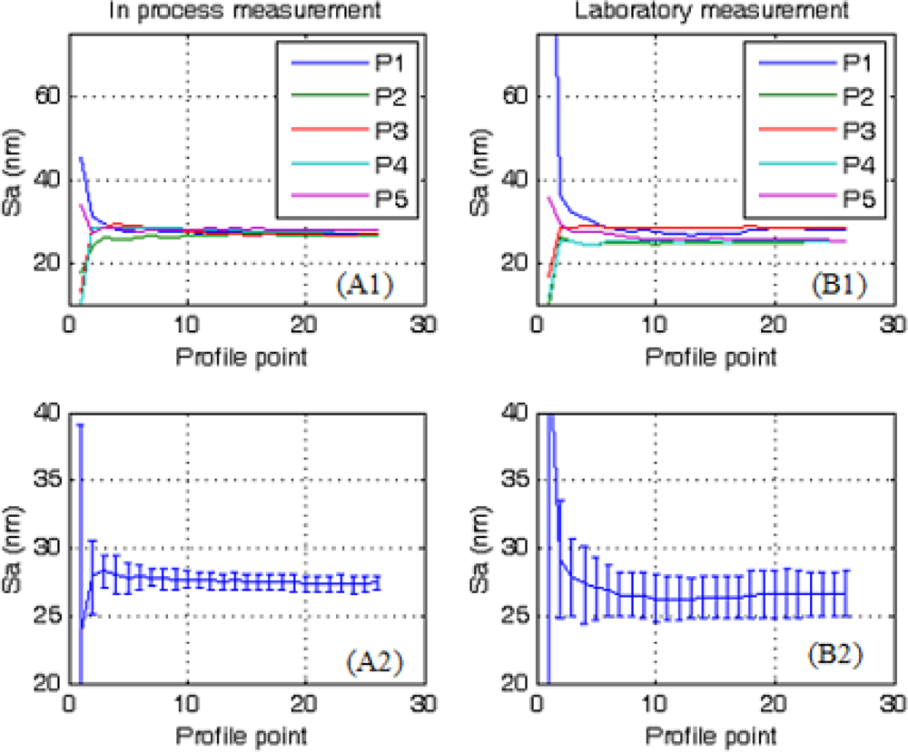
- - Sample in the laboratory is measured and roughness results are compared with those previously obtained to demonstrate the possibility or not to use the AFM as portable instrument in the fabrication of a solar cell industry.
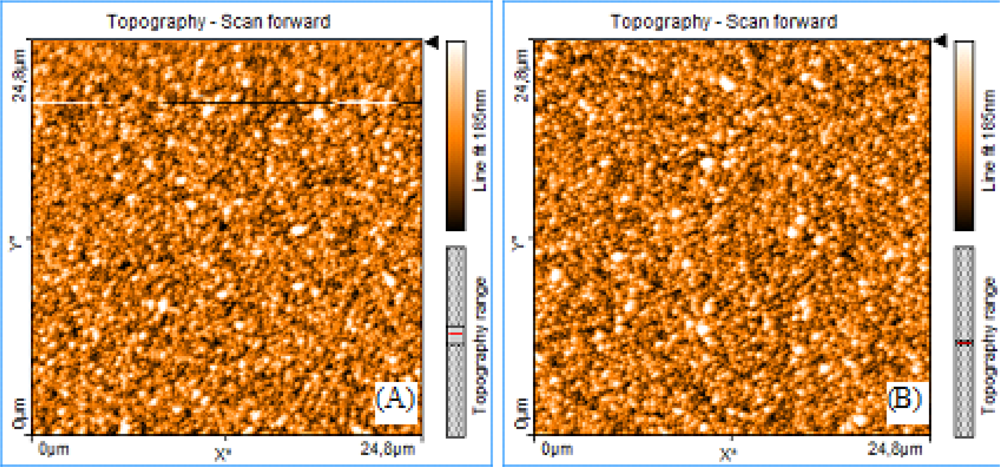
3. Results and Discussion
4. Conclusions
Acknowledgments
References and Notes
- Smith, G.T. Industrial Metrology: Surfaces and Roundness; Springer-Verlag: London, UK, 2002. [Google Scholar]
- Dagnall, M.A. Exploring Surface Texture; Rank Taylor Hobson Limited: Leicester, UK, 1986. [Google Scholar]
- Whitehouse, D.J. Handbook of Surface and Nanometrology; Institute of Physics Publishing: London, UK, 2003. [Google Scholar]
- Eckardt, T.; Bewilogua, K.; van der Kolk, G.; Hurkmans, T.; Trinh, T.; Fleisher, W. Improving tribological properties of sputtered boron carbide coatings by process modifications. Surf. Coat. Tech 2000, 126, 69–75. [Google Scholar]
- Begand, S.; Oberbach, T.; Herrmann, M.; Sempf, K. Surface properties after ageing of dispersion ceramic and its influence on strength. Key Eng. Mat 2009, 396–398, 157–160. [Google Scholar]
- Gubbels, G.; van Venrooy, B.; Bosch, A.J.; Senden, R. Rapidly solidified aluminium for optical applications. Proceedings of the SPIE—The international society for optical engineering, Marseille, France; 2008; pp. 70183–70192. [Google Scholar]
- Masuda, J.; Yan, J.; Tashiro, T.; Fukase, Y.; Zhou, T.; Kuriyagawa, T. Microstructural and topographical changes of Ni-P plated moulds in glass lens pressing. Int. J. Surf. Sci. Eng 2009, 3, 86–102. [Google Scholar]
- Sakata, F.Y.; Santo, A.M.E.; Miyakawa, W.; Riva, R.; Lima, M.S.F. Influence of laser surface texturing on surface microstructure and mechanical properties of adhesive joined steel sheets. Surf. Eng 2009, 25, 180–186. [Google Scholar]
- Brown, L.; Blunt, L. Surface metrology for the automotive industry. In Proceedings of Inaugural Automotive Researchers Conference, Huddersfield, UK; 2008. [Google Scholar]
- Danzebrink, H.U.; Koenders, L.; Wikening, G.; Yacoot, A.; Kunzmann, H. Advances in scanning force microscopy for dimensional metrology. CIRP Ann.-Manuf. Technol 2006, 55, 841–878. [Google Scholar]
- Nanosurf. Available online: http://www.nanosurf.com/default.cfm?curr_navi=11&curr_content=11&spr=en (Access on 22 Decemeber 2009).
- DME Scanning Probe Microscopes. Available online: http://www.dme-spm.com/ds95.html (Access on 26 December 2009).
- Krc, J.; Zeman, M.; Kluth, O.; Smole, F.; Topic, M. Effect of surface roughness of ZnO: Al films on light scattering in hydrogenated amorphous silicon solar cells. Thin solid films 2003, 426, 296–304. [Google Scholar]
- Escarré, J.; Villar, F.; Fonrodona, M.; Soler, D.; Asensi, J.M.; Bertomeu, J.; Andreu, J. Optical analysis of textured plastic substrates to be used in thin silicon solar cells. Solar Energ. Mater. Solar Cells 2005, 87, 333–341. [Google Scholar]
- Nanosensors. Available online: http://www.nanosensors.com/PPP-NCLR.htm (Access on 11 December 2009).
- Image Metrology. http://www.imagemet.com/WebHelp/spip.htm#roughness_parameters.htm (Access on 22 December 2009).


| Fabrication area | Laboratory area | |
|---|---|---|
| Sa (nm) | 27.4 ± 0.6 | 26.6 ± 1.7 |
| Sq (nm) | 34.9 ± 0.6 | 34.1 ± 2.4 |
© 2010 by the authors; licensee MDPI, Basel, Switzerland. This article is an open-access article distributed under the terms and conditions of the Creative Commons Attribution license ( http://creativecommons.org/licenses/by/3.0/).
Share and Cite
González-Jorge, H.; Alvarez-Valado, V.; Valencia, J.L.; Torres, S. In Situ Roughness Measurements for the Solar Cell Industry Using an Atomic Force Microscope. Sensors 2010, 10, 4002-4009. https://doi.org/10.3390/s100404002
González-Jorge H, Alvarez-Valado V, Valencia JL, Torres S. In Situ Roughness Measurements for the Solar Cell Industry Using an Atomic Force Microscope. Sensors. 2010; 10(4):4002-4009. https://doi.org/10.3390/s100404002
Chicago/Turabian StyleGonzález-Jorge, Higinio, Victor Alvarez-Valado, Jose Luis Valencia, and Soledad Torres. 2010. "In Situ Roughness Measurements for the Solar Cell Industry Using an Atomic Force Microscope" Sensors 10, no. 4: 4002-4009. https://doi.org/10.3390/s100404002