One-Dimensional Oxide Nanostructures as Gas-Sensing Materials: Review and Issues

Abstract
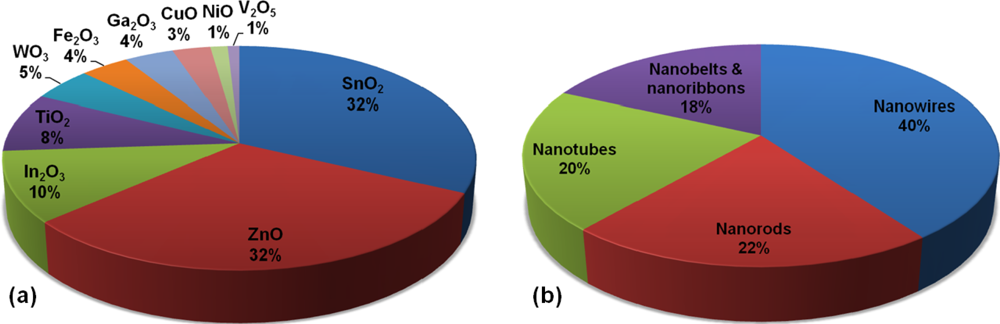
:1. Introduction
2. Types of Gas-Sensor Structure Based Upon 1D Oxide Nanostructures
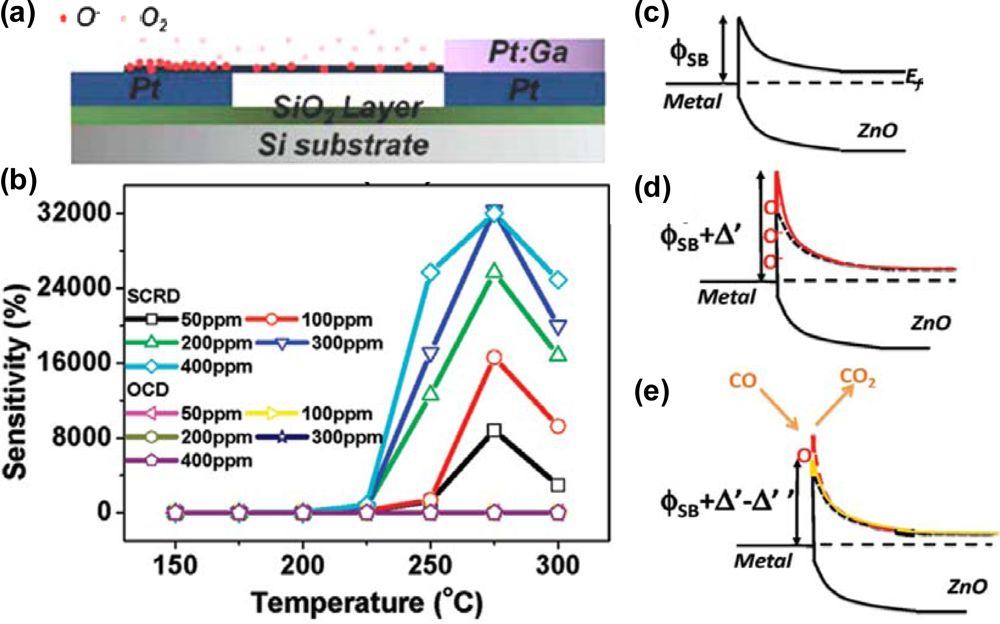
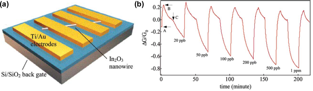
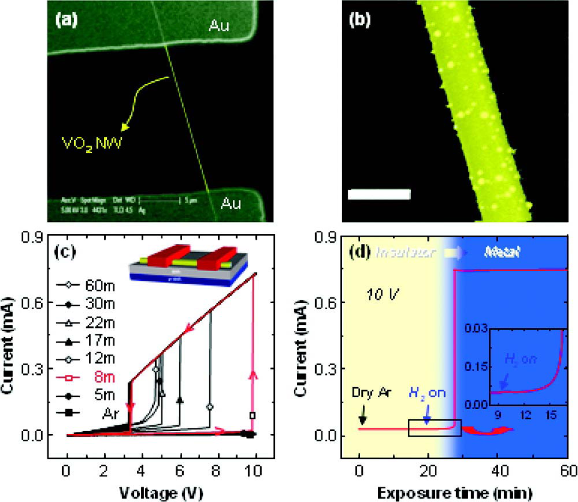
2.1. Single 1D Nanostructure Gas Sensors
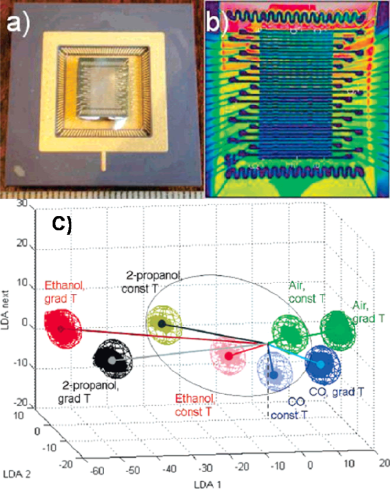
2.2. Multiple and Self-Assembled 1D Nanostructures
3. Critical Issues
3.1. Long-Term Stability
3.2. Gas Selectivity
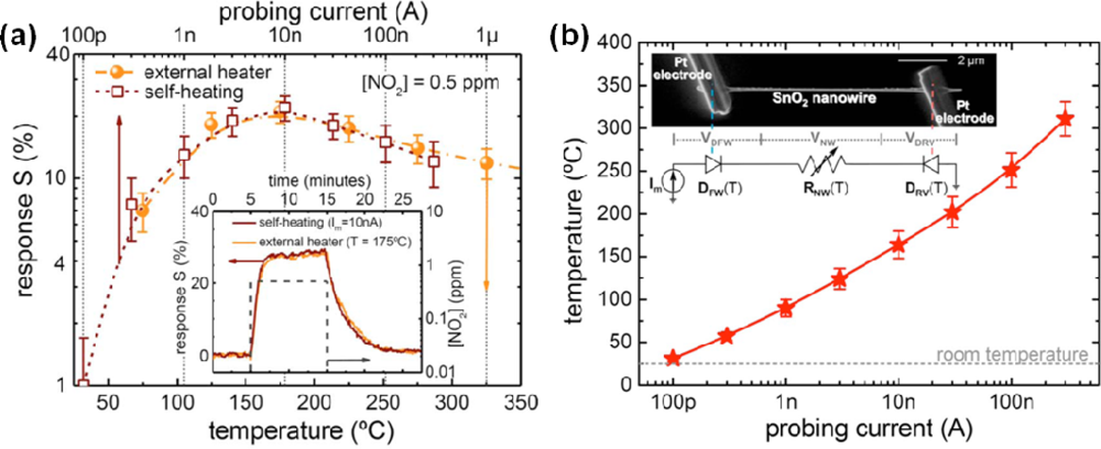
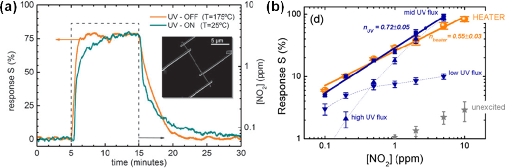
3.3. Room-Temperature Operation
4. Summary
Acknowledgments
References and Notes
- Seiyama, T.; Kato, A.; Fulishi, K.; Nagatani, M. A new detector for gaseous components using semiconductive thin films. Anal. Chem 1962, 34, 1502–1503. [Google Scholar]
- Law, M.; Kind, H.; Messer, B.; Kim, F.; Yang, P.D. Photochemical sensing of NO2 with SnO2 nanoribbon nanosensors at room temperature. Angew. Chem. Int. Ed 2002, 41, 2405–2408. [Google Scholar]
- Arnold, M.S.; Avouris, P.; Pan, Z.W.; Wang, Z.L. Field-effect transistors based on single semiconducting oxide nanobelts. J. Phys. Chem. B 2003, 107, 659–663. [Google Scholar]
- Cheng, Y.; Xiong, P.; Fields, L.; Zheng, J.P.; Yang, R.S.; Wang, Z.L. Intrinsic characteristics of semiconducting oxide nanobelt field-effect transistors. Appl. Phys. Lett 2006, 89, 093114. [Google Scholar]
- Andrei, P.; Fields, L.L; Zheng, J.P.; Cheng, Y.; Xiong, P. Modeling and simulation of single nanobelt SnO2 gas sensors with FET structure. Sens. Actuat. B 2007, 128, 226–234. [Google Scholar]
- Qian, L.H.; Wang, K.; Li., Y.; Fang, H.T.; Lu, Q.H.; Ma, X. L. CO sensor based on Au-decorated SnO2 nanobelt. Mater. Chem. Phys 2006, 10, 82–84. [Google Scholar]
- Kuang, Q.; Lao, C.S.; Wang, Z.L.; Xie, Z.X.; Zheng, L.S. High-sensitivity humidity sensor based on a single SnO2 nanowire. J. Am. Chem. Soc 2007, 129, 6070–6071. [Google Scholar]
- Kuang, Q.; Lao, C.S.; Li, Z.; Liu, Y.Z.; Xie, Z.X.; Zheng, L.S.; Wang, Z.L. Enhancing the photon- and gas-sensing properties of a single SnO2 nanowire based nanodevice by nanoparticle surface functionalization. J. Phys. Chem. C 2008, 112, 11539–11544. [Google Scholar]
- Kumar, V.; Sen, S.; Muthe, K.P.; Gaur, N.K.; Gupta, S.K.; Yakhmi, J.V. Copper doped SnO2 nanowires as highly sensitive H2S gas sensor. Sens. Actuat. B 2009, 138, 587–590. [Google Scholar]
- Wei, T.Y.; Yeh, P.H.; Lu, S.Y.; Wang, Z.L. Gigantic enhancement in sensitivity using Schottky contacted nanowire nanosensor. J. Am. Chem. Soc 2009, 131, 17690–17695. [Google Scholar]
- Zhou, J.; Gu, Y.; Hu, Y.; Mai, W.; Yeh, P. H.; Bao, G.; Sood, A. K.; Polla, D. L.; Wang, Z. L. Gigantic enhancement in response and reset time of ZnO UV nanosensor by utilizing Schottky contact and surface functionalization. Appl. Phys. Lett 2009, 94, 191103. [Google Scholar]
- Yeh, P. H.; Li, Z.; Wang, Z. L. Schottky-gated probe-free ZnO nanowire biosensor. Adv. Mater 2009, 21, 4975–4978. [Google Scholar]
- Liao, L.; Lu, H.B.; Li, J.C.; Liu, C.; Fu, D.J.; Liu, Y.L. The sensitivity of gas sensor based on single ZnO nanowire modulated by helium ion radiation. Appl. Phys. Lett 2007, 91, 173110. [Google Scholar]
- Choi, S.H.; Yee, S.M.; Ji, H.J.; Choi, J.W.; Cho, Y.S.; Kim, G.T. Smart gas sensor and noise properties of single ZnO nanowire. Jpn. J. Appl. Phys 2009, 48, 06FD13. [Google Scholar]
- Li, C.; Zhang, D.H.; Liu, X.L.; Han, S.; Tang, T.; Han, J.; Zhou, C.W. In2O3 nanowires as chemical sensors. Appl. Phys. Lett 2003, 82, 1613–1615. [Google Scholar]
- Zhang, D.H.; Liu, Z.Q.; Li, C.; Tang, Tao; Liu, X.L.; Han, S.; Lei, B.; Zhou, C.W. Detection of NO2 down to ppb levels using individual and multiple In2O3 nanowire devices. Nano Lett 2004, 4, 1919–1924. [Google Scholar]
- Zeng, Z.M.; Wang, K.; Zhang, Z.X.; Chen, J.J.; Zhou, W.L. The detection of H2S at room by using individual indium oxide nanowire transistors. Nanotechnology 2009, 20, 045503. [Google Scholar]
- Kolmakov, A.; Zhang, Y.; Cheng, G.; Moskovits, M. Detection of CO and O2 using Tin oxide nanowire sensors. Adv. Mater 2003, 15, 997–1000. [Google Scholar]
- Zhang, Y.; Kolmakov, A.; Chretien, S.; Metiu, H.; Moskovits, M. Control of catalystic reactions at the surface of a metal oxide nanowire by manipulating electron density inside it. Nano Lett 2004, 4, 403–407. [Google Scholar]
- Zhang, Y.; Kolmakov, A.; Lilach, Y.; Moskovits, M. Electronic control of chemistry and catalysis at the surface of an individual oxide nanowire. J. Phys. Chem. B 2005, 19, 1923–1929. [Google Scholar]
- Kolmakov, A.; Klenov, D.O.; Lilach, Y.; Stemmer, S.; Moskovits, M. Enhanced gas sensing by individual SnO2 nanowires and nanobelts functionalized with Pd catalyst particles. Nano Lett 2005, 5, 667–673. [Google Scholar]
- Chen, X.H.; Moskovits, M. Observing catalysis through the agency of the participating electrons: Surface-chemistry-induced current changes in a tin oxide nanowire decorated with silver. Nano Lett 2007, 7, 807–812. [Google Scholar]
- Strelcov, E.; Lilach, Y.; Kolmakov, A. Gas sensor based on metal-insulator transition in VO2 nanowire thermistor. Nano Lett 2009, 9, 2322–2326. [Google Scholar]
- Baik, J.M.; Kim, M.H.; Larson, C.; Yavuz, C.T.; Stucky, G.D; Wodtke, A.M.; Moskovits, M. Pd-sensitized single vanadium oxide nanowires: Highly responsive hydrogen sensing based on the metal-insulator transition. Nano Lett 2009, 9, 3980–3984. [Google Scholar]
- Li, Q.H.; Laing, Y.X.; Wan, Q.; Wang, T.H. Oxygen sensing characteristics of individual ZnO nanowire transistors. Appl. Phys. Lett 2004, 85, 6389–6391. [Google Scholar]
- Feng, P.; Xue, Y.X.; Liu, Y.G.; Wan, Q.; Wang, T.H. Achieving fast oxygen response in individual β-Ga2O3 nanowires by ultraviolet illumination. Appl. Phys. Lett 2006, 89, 112114. [Google Scholar]
- Xue, Y.X.; Feng, P.; Wang, Y.G.; Wang, T.H. Extremely high oxygen sensing of individual ZnSnO3 nanowires arising from grain boundary barrier modulation. Appl. Phys. Lett 2007, 91, 022111. [Google Scholar]
- Hernandez-Ramirez, F.; Tarancon, A.; Casals, O.; Arbiol, J.; Romano-Rodriguez, A.; Morante, J.R. High response and stability in CO and humidity measures using a single SnO2 nanowire. Sens. Actuat. B 2009, 121, 3–17. [Google Scholar]
- Prades, J.D.; Jimenez-Diaz, R.; Hernandez-Ramirez, F.; Barth, S.; Cirera, A.; Romano-Rodriguez, A.; Mathur, S.; Morante, J.R. Ultralow power consumption gas sensors based on self-heated individual nanowires. Appl. Phys. Lett 2008, 93, 123110. [Google Scholar]
- Prades, J.D.; Jimenez-Diaz, R.; Manzanares, M.; Hernandez-Ramirez, F.; Cirera, A.; Romano-Rodriguez, A.; Mathur, S.; Morante, J.R. A model for the response towards oxidizing gases of photoactivated sensors based on individual SnO2 nanowires. Phys. Chem. Chem. Phys 2009, 11, 10881–10889. [Google Scholar]
- Prades, J.D.; Jimenez-Diaz, R.; Hernandez-Ramirez, F.; Barth, S; Cirera, A.; Romano-Rodriguez, A.; Mathur, S.; Morante, J.R. Equivalence between thermal and room temperature UV light-modulated responses of gas sensors based on individual SnO2 nanowires. Sens. Actuat. B 2009, 140, 337–342. [Google Scholar]
- Heo, Y.W.; Tien, L.C.; Norton, D.P.; Kang, B.S.; Ren, F.; Gila, B.P.; Pearton, S.J. Electrical transport properties of single ZnO nanorods. Appl. Phys. Lett 2004, 85, 2002–2004. [Google Scholar]
- Wang, H.T.; Kang, B.S.; Ren, F.; Tien, L.C.; Sadik, P.W.; Norton, D.P.; Pearton, S.J.; Lin, J.S. Hydrogen-selective sensing at room temperature with ZnO nanorods. Appl. Phys. Lett 2005, 86, 243503. [Google Scholar]
- Zhang, N.; Yu, K.; Li, L.J.; Zhu, Z.Q. Investigation of electrical and ammonia sensing characteristics of Schottky barrier diode based on a single ultra-long ZnO nanorod. Appl. Surf. Sci 2008, 254, 5736–5740. [Google Scholar]
- Lupan, O.; Chai, G; Chow, L. Novel hydrogen gas sensor based on single ZnO nanorod. Microelectr. Eng 2008, 85, 2220–2225. [Google Scholar]
- Liu, Y.; Liu, M. Growth of aligned square-shaped SnO2 tube arrays. Adv. Mater 2005, 15, 57–62. [Google Scholar]
- Rout, C.S.; Kulkarni, G.U.; Rao, C.N.R. Room temperature hydrogen and hydrocarbon sensors based on single nanowires of metal oxides. J. Phys. D 2007, 40, 2777–2782. [Google Scholar]
- Tresback, J.S.; Padture, N.P. Low-temperature gas sensing in individual metal-oxide-metal heterojunction nanowires. J. Mater. Res 2008, 23, 2047–2052. [Google Scholar]
- Liao, L.; Mai, H.X.; Yuan, Q.; Lu, H.B.; Li, J.C.; Liu, C.; Yan, C.H.; Shen, Z.X.; Yu, T. Single CeO2 nanowire gas sensor supported with Pt nanocrystals: Gas sensitivity, surface bond states, and chemical mechanism. J. Phys. Chem. C 2008, 112, 9061–9065. [Google Scholar]
- Lee, J.S.; Kim, Y.J.; Kuk, B.; Geyer, A.; Platt, U. Simultaneous measurements of atmospheric pollutants and visibility with a long-path DOAS system in urban areas. Environ. Monit. Assess 2005, 104, 281–293. [Google Scholar]
- Courtillot, I; Morville, J.; Motto-Ros, V.; Romanini, D. Sub-ppb NO2 detection by optical feedback cavity-enhanced absorption spectroscopy with a blue diode laser. Appl. Phys. B-Lasers Opt 2006, 85, 407–412. [Google Scholar]
- Wang, L.M.; Zhang, J.S. Detection of nitrous acid by cavity ring down spectroscopy. Environ. Sci. Tech 2000, 34, 4221–4227. [Google Scholar]
- Simeonsson, J.B.; Elwood, S.A.; Niebes, M.; Carter, R.; Peck, A. Trace detection of NO and NO2 by photoionization and laser induced fluorescence techniques. Anal. Chim. Acta 1999, 397, 33–41. [Google Scholar]
- Pandey, S.K.; Kim, K.H. Review of Methods for the Determination of Reduced Sulfur Compounds (RSCs) in Air. Environ. Sci. Tech 2009, 43, 3020–3029. [Google Scholar]
- Cruz, L.P.S.; Campos, V.P. Sampling and analytical methods for atmospheric reduced sulphur compounds. Quim. Nova 2008, 31, 1180–1189. [Google Scholar]
- Kim, K.H. Performance characterization of the GC/PFPD for H2S, CH3SH, DMS, and DMDS in air. Atmos. Environ 2005, 39, 2235–2242. [Google Scholar]
- Besson, J.P.; Schilt, S.; Rochat, E.; Thevenaz, L. Ammonia trace measurements at ppb level based on near-IR photoacoustic spectroscopy. Appl. Phys. B-Lasers Opt 2006, 85, 323–328. [Google Scholar]
- Li, Y.Q.; Schwab, J.J.; Demerjian, K.L. Measurements of ambient ammonia using a tunable diode laser absorption spectrometer: Characteristics of ambient ammonia emissions in an urban area of New York City. J. Geophys. Res 2006, 111, D10S02. [Google Scholar]
- Ahn, M.-W.; Park, K.-S.; Heo, J.-H.; Kim, D.-W.; Choi, K. J.; Park, J.-G. On-chip fabrication of ZnO-nanowire gas sensor with high gas sensitivity. Sens. Actuat. B 2009, 138, 168–173. [Google Scholar]
- Choi, Y.-J.; Hwang, I.-S.; Park, J.-G.; Choi, K. J.; Park, J.-H.; Lee, J.-H. Novel fabrication of an SnO2 nanowire gas sensor with high sensitivity. Nanotechnology 2008, 19, 095508. [Google Scholar]
- Ahn, M.-W.; Park, K.-S.; Heo, J.-H.; Park, J.-G.; Kim, D.-W.; Choi, K. J.; Lee, J.-H.; Hong, S.-H. Gas sensing properties of defect-controlled ZnO-nanowire gas sensor. Appl. Phys. Lett 2008, 93, 263103. [Google Scholar]
- Peng, K.-Q.; Wang, X.; Lee, S.-T. Gas sensing properties of single crystalline porous silicon nanowires. Appl. Phys. Lett 2009, 95, 243112. [Google Scholar]
- Hernandez-Ramirez, F.; Prades, J.D.; Jimenez-Diaz, R.; Fischer, T.; Romano-Rodriguez, A.; Mathur, S.; Morante, J.R. On the role of individual metal oxide nanowires in the scaling down of chemical sensors. Phys. Chem. Chem. Phys 2009, 11, 7105–7110. [Google Scholar]
- Sysoev, V.V.; Schneider, T.; Goschnick, J.; Kiselev, I.; Habicht, W.; Hahn, H.; Strelcov, E.; Kolmakov, A. Percolating SnO2 nanowire network as a stable gas sensor: Direct comparison of long-term performance versus SnO2 nanoparticle films. Sens. Actuat. B 2009, 139, 699–703. [Google Scholar]
- Zeng, W.; Liu, T.; Wang, Z.; Tsukimoto, S.; Saito, M.; Ikuhara, Y. Selective detection of Formaldehyde gas using a Cd-doped TiO2-SnO2 sensor. Sensors 2009, 9, 9029–9038. [Google Scholar]
- Vander Wal, R.L.; Berger, G.M.; Kulis, M.J.; Hunter, G.W.; Xu, J.C.; Evans, L. Synthesis methods, microscopy characterization and device integration of nanoscale metal oxide semiconductors for gas sensing. Sensors 2009, 9, 7866–7902. [Google Scholar]
- Flueckiger, J.; Ko, F.K.; Cheung, K.C. Microfabricated formaldehyde gas sensors. Sensors 2009, 9, 9196–9215. [Google Scholar]
- Hagleitner, C.; Hierlemann, A.; Lange, D.; Kummer, A.; Kerness, N.; Brand, O.; Baltes, H. Smart single-chip gas sensor microsystem. Nature 2001, 414, 293–296. [Google Scholar]
- Sysoev, V.V.; Goschnick, J.; Schneider, T.; Strelcov, E.; Kolmakov, A. A gradient microarray electronic nose based on percolating SnO2 nanowire sensing elements. Nano Lett 2007, 7, 3182–3188. [Google Scholar]
- Sysoev, V.V.; Button, B.K.; Wepsiec, K.; Dmitriev, S.; Kolmakov, A. Toward the nanoscopic “electronic nose”: hydrogen vs carbon monoxide discrimination with an array of individual metal oxide nano- and mesowire sensors. Nano Lett 2006, 6, 1584–1588. [Google Scholar]
- McAlpine, M.C.; Ahmad, H.; Wang, D.; Heath, J.R. Highly ordered nanowire arrays on plastic substrates for ultrasensitive flexible chemical sensors. Nat. Mater 2007, 6, 379–384. [Google Scholar]
- Peng, L.; Zhao, Q.; Wang, D.; Zhai, J.; Wang, P.; Pang, S.; Xie, T. Ultraviolet-assisted gas sensing: A potential formaldehyde detection approach at room temperature based on zinc oxide nanorods. Sens. Actuat. B 2009, 139, 80–85. [Google Scholar]
- Fan, Z.; Lu, J.G. Gate-refreshable nanowire chemical sensors. Appl. Phys. Lett 2005, 86, 123510. [Google Scholar]


| Target gas | Material | Sensor type | Detection limit (Temp.) | Sensitivity (Conc.) | Response time | Ref. |
|---|---|---|---|---|---|---|
| NO2 | SnO2 nanoribbon | Resistor | 2 ppm (25 °C) | 7 (100 ppm) | ∼1 min | [2] |
| NO2 | SnO2 nanowire | Resistor | <0.1 ppm (25 °C) | 1 (10 ppm) | ∼ 1 min | [31] |
| NO2 | In2O3 nanowire | FET | 0.5 ppm (25 °C) | 106 (100 ppm) | 5 s | [15] |
| NO2 | In2O3 nanowire | FET | 0.02 ppm (25 °C) | 0.8 (1 ppm) | 15 min | [16] |
| H2 | SnO2 nanobelt | FET | 0.2% (25 °C) | 0.17 (0.2%) | N/A | [4] |
| H2 | SnO2 nanowire | FET | <1 ppm (200 °C) | 4 (1 ppm) | ∼50 s | [21] |
| H2 | ZnO nanorod | Resistor | 200 ppm (25 °C) | 0.04 (200 ppm) | 30−40 s | [35] |
| H2 | VO2 nanowire | Resistor | N/A (50 °C) | 1000 (100%) | ∼10 min | [24] |
| H2 | WO2.72 nanowire | Resistor | < 100 ppm (25 °C) | 22 (1,000 ppm) | 40 s | [37] |
| CO | SnO2 nanobelt | Resistor | 5 ppm (400 °C) | 7 (250 ppm) | 30 s | [6] |
| CO | SnO2 nanowire | FET | 100 ppm (25 °C) | 15 (500 ppm) | ∼10 min | [8] |
| CO | ZnO nanowire | Resistor | <50 ppm (275 °C) | 3200 (400 ppm) | ∼50 min | [10] |
| CO | NiO nanowire | Resistor | N/A (150 °C) | 0.25 (800 ppm) | ∼2 h | [38] |
| CO | CeO2 nanowire | Resistor | <10 ppm (25 °C) | 2 (200 ppm) | ∼10 s | [39] |
| H2S | SnO2 nanowire | Resistor | <1 ppm (150 °C) | 6 × 10⁶ (50 ppm) | N/A | [9] |
| H2S | ZnO nanowire | Resistor | N/A (25 °C) | 8 (300 ppm) | ∼50 s | [13] |
| H2S | In2O3 nanowire | FET | 1 ppm (25 °C) | 1 (20 ppm) | 48 s | [17] |
| Ethanol | SnO2 nanotube | Resistor | N/A (400 °C) | 20 (7.8%) | ∼80 s | [36] |
| O2 | β-Ga2O3 nanowire | Resistor | <50 ppm (25 °C) | 20 (50 ppm) | 1 s | [26] |
© 2010 by the authors; licensee MDPI, Basel, Switzerland. This article is an open-access article distributed under the terms and conditions of the Creative Commons Attribution license ( http://creativecommons.org/licenses/by/3.0/).
Share and Cite
Choi, K.J.; Jang, H.W. One-Dimensional Oxide Nanostructures as Gas-Sensing Materials: Review and Issues. Sensors 2010, 10, 4083-4099. https://doi.org/10.3390/s100404083
Choi KJ, Jang HW. One-Dimensional Oxide Nanostructures as Gas-Sensing Materials: Review and Issues. Sensors. 2010; 10(4):4083-4099. https://doi.org/10.3390/s100404083
Chicago/Turabian StyleChoi, Kyoung Jin, and Ho Won Jang. 2010. "One-Dimensional Oxide Nanostructures as Gas-Sensing Materials: Review and Issues" Sensors 10, no. 4: 4083-4099. https://doi.org/10.3390/s100404083