Study of Temperature Characteristics of Micromachined Suspended Coplanar Waveguides for Biosensing Applications

Abstract
: In the recent development on biosensors, coplanar waveguide based microwave dielectric sensors have been attracting more and more attentions. In this paper, microwave performance of a suspended coplanar waveguide subject to temperature variations, particularly in a small range, is studied. The prototype is realized through a MEMS fabrication foundry. The thermal transfer analysis of the device is conducted using finite element method, and the microwave properties of the device are characterized. One of the results shows that at 20 GHz, the S11 has decreased by 7.4%, and S21 has increased by 3.5% when the voltage applied to the heaters varies from 9 V to 29 V.1. Introduction
Microwave biosensors usually don’t require the biosamples to be optically or chemically altered, which is a big advantage compared with optical and chemical biosensors. Micromachined coplanar waveguides have been used to realize biosensors due to their smaller size and high performance [1,2]. Several examples of using coplanar waveguides as microsensors are summarized as follows. A gas sensor composed of a suspended micromachined coplanar waveguide with carbon nanotubes as dielectric materials was reported in [3], which was based on gas-induced variations in dielectric permittivity of carbon nanotubes. Demonstration of a Gaubau transmission line for biosensor applications has been reported in [4], which was constructed on a coplanar waveguide. A wide-bandwidth, high-sensitivity particle sensing and cell counting device in a microfluidic system was presented using coplanar waveguide technology [5]. Distributed transmission lines have been utilized to serve as biosensors, which have the advantage of intensified interactions between electromagnetic waves and biosamples in slow-wave structures [6–8]. In the biosensing applications, it is quite often that the temperature of biosamples changes due to chemical reactions or electrical heating from the sensor itself. Thus study of temperature characteristics of coplanar waveguide is important to understand the impact on microwave performances of the sensors upon temperature variations. It is known that high temperature will have some effects on the performance of the coplanar waveguides, as the series resistance of the signal line varies due to temperature variations [9]. Many previous theoretical and experimental studies described temperature-dependence of the traditional coplanar waveguides [10–12]. However most of the above investigations were based on evenly temperature rising of the CPW structures, or based on self-heating by the RF signal passing through the CPW [13,14]. In many real cases, the temperature rising happens just in parts of the CPW structure where the heat sources are some adjacent electronic circuits. To the best of author’s knowledge, there is no previous scientific literature reported on investigation of the CPW performance under external localized heating.
In this paper, a new structure that consists of a suspended CPW and two silicon heaters adjacent to the ground plane has been designed for the purpose of investigating microwave performances of the CPW subject to the localized heating. The structure has been fabricated through a MEMS fabrication process and subsequently characterized using microwave equipments. Temperature profiles of the heaters and CPW have been modeled using a finite element software. The paper is structured as follows: section 2 of the paper describes the design, fabrication, and thermal transfer modeling of the device. Microwave measurements of the device are reported in section 3. Finally in section 4 some conclusion remarks are made.
2. Design, Fabrication, and Thermal Modeling of the Device
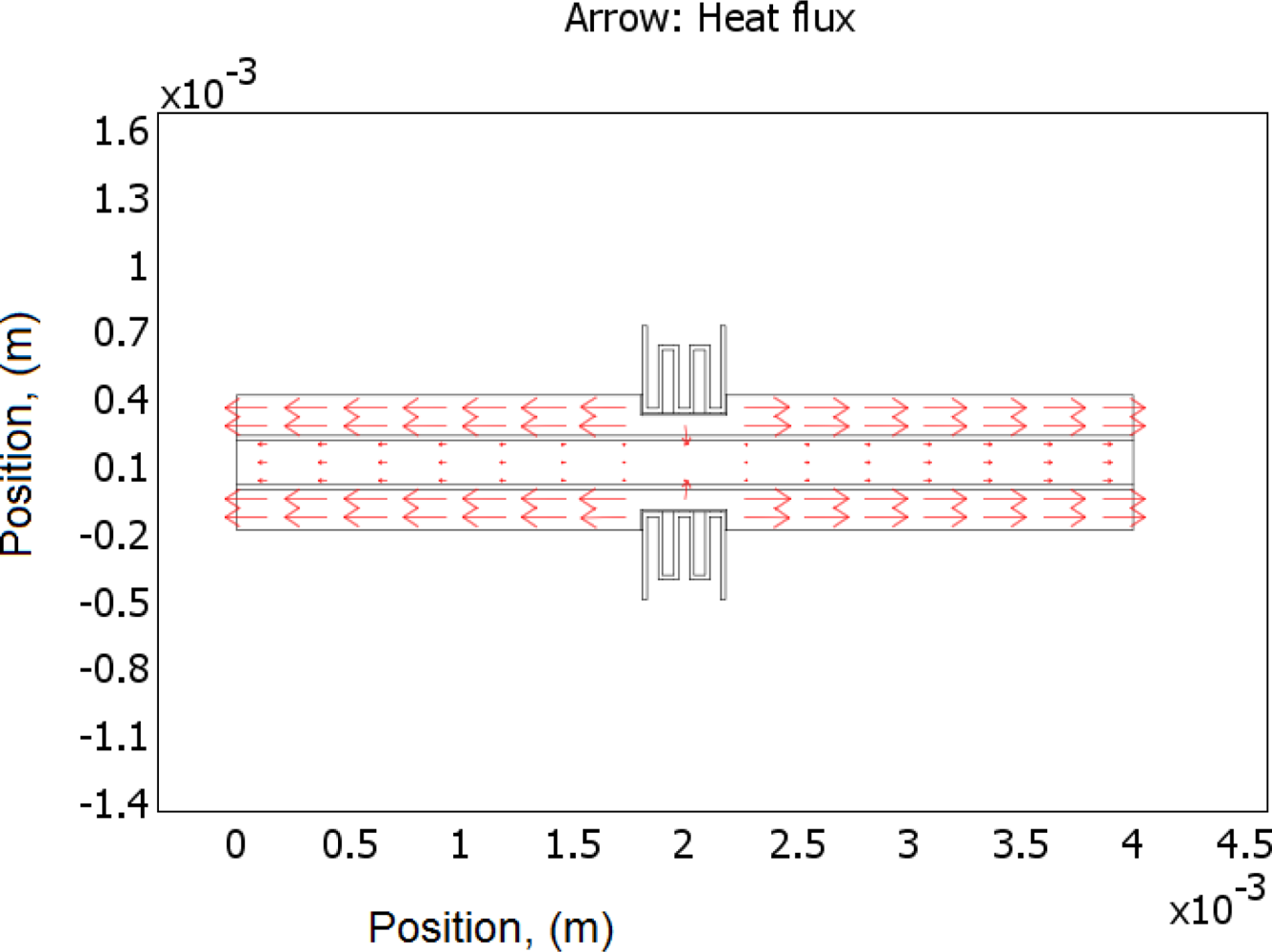
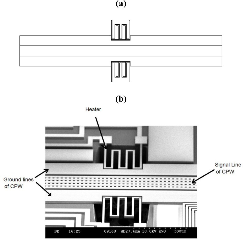
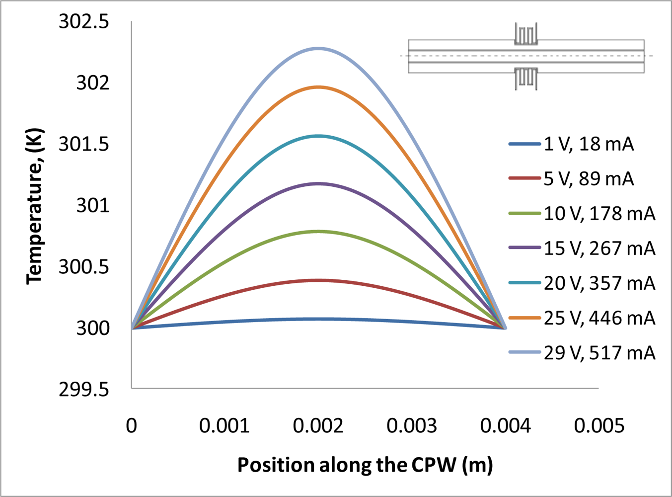
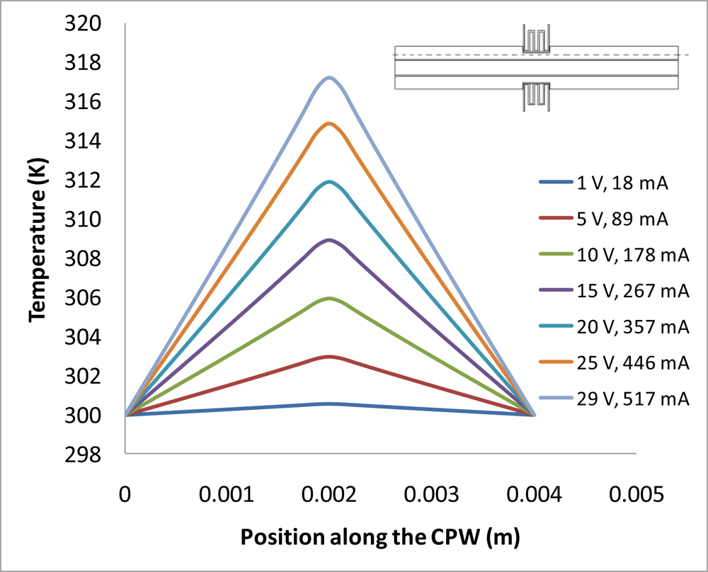
In order to study the temperature impact on the CPW caused by surrounding heat sources. A test structure that consists of a suspended CPW and two suspended spring-shaped silicon heaters located on both sides of the CPW symmetrically has been designed. The schematic graph of the test structure is shown in Figure 1(a). In principle, heat is generated by joule heating of the two silicon resistors through which electrical current flows, subsequently temperature of the ground plane of the CPW will increase through heat transfer mechanisms, and the temperature of the signal line of CPW increases as well. However due to the localized heating, the temperature distributions along the ground plane and signal line of the CPW are not the same. Prototype of the test structure has been realized through silicon-on-insulator based MEMS foundry process. The fabrication procedure is summarized as follows: a silicon-on-insulator wafer is prepared and the silicon layer has been patterned. Next, the surface of the silicon layer has been metalized for the purpose of creating electrical conductors and increasing optical reflectivity of the surface. In this case, metallization is used for increasing the conductivity of the coplanar waveguide. The heater structure is not coated with the metal. Finally the wafer has been back-etched from the bottom side, so that the structures in the silicon layer can be released. This step is used to realize the suspended CPW and heaters. The fabricated structures have been examined by the scanning electron microscope and Figure 1(b) shows one of the SEM images. Small holes are designed in the signal line to reduce the initial stress during the releasing process.
Since the structure is very small, it is very difficult to measure its temperature using thermometers. Theoretical analysis of the temperature distribution has been conducted based on the finite element method (FEM); here a FEM software was used to perform the electrical-thermal transfer analysis. Joule heating in microdevice is a well known phenomenon that has been studied extensively, particularly when people were looking at electrothermal actuators [15,16]. One dimensional analytical thermal modelling can be used to simulate structures that have uniform width and thickness, for example in [15]. However for thermal transfer problem in complex structures, such as for the case reported in this paper, two-dimensional thermal transfer analysis has to be performed using finite element method. For the spring-shaped heater structure in the Figure 1, the temperature of the heater itself and different part of the CPW is governed by the heat conduction transfer equation:
3. Microwave Measurements
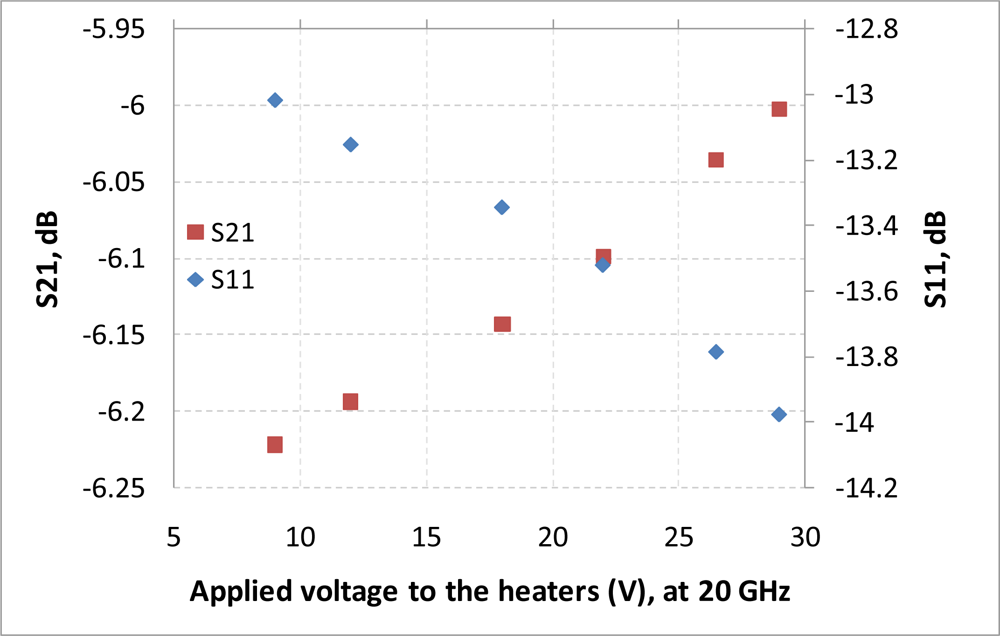
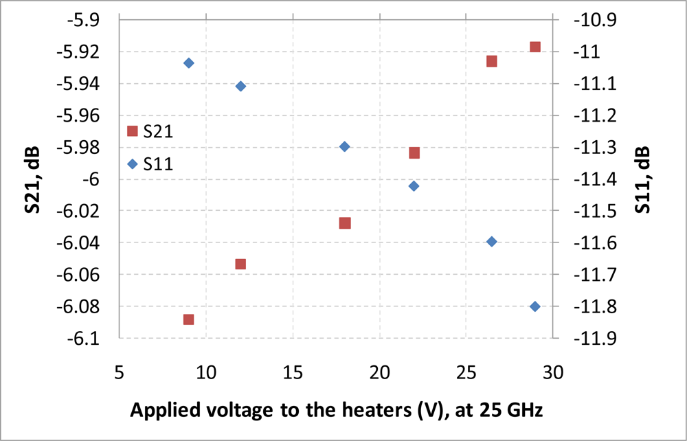
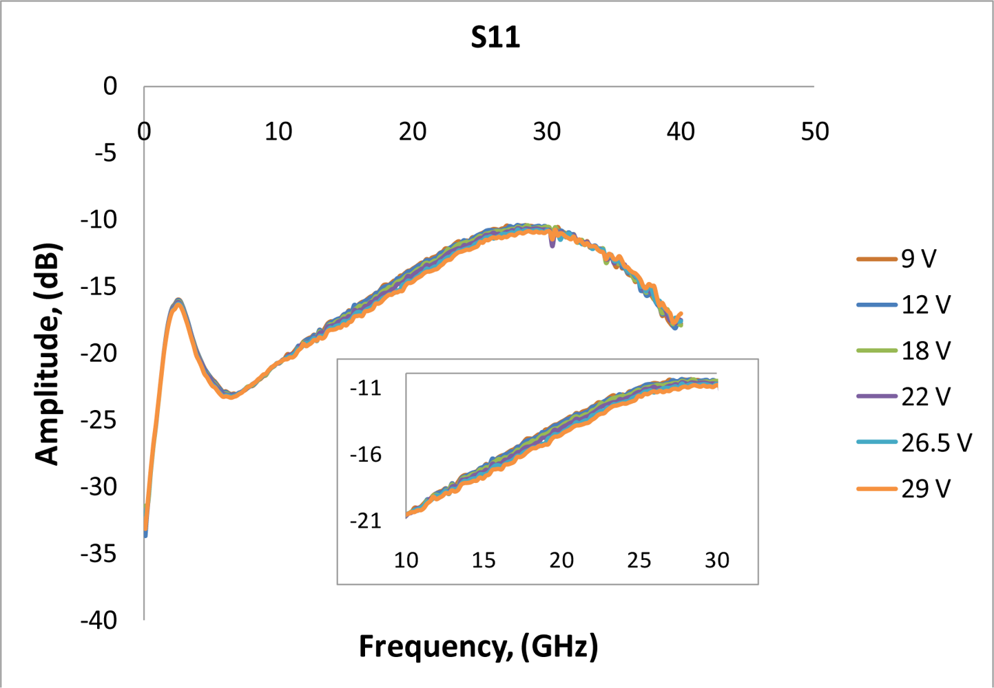
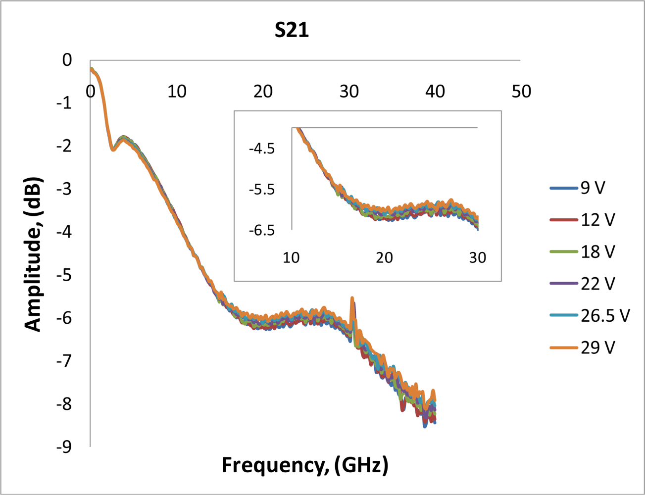
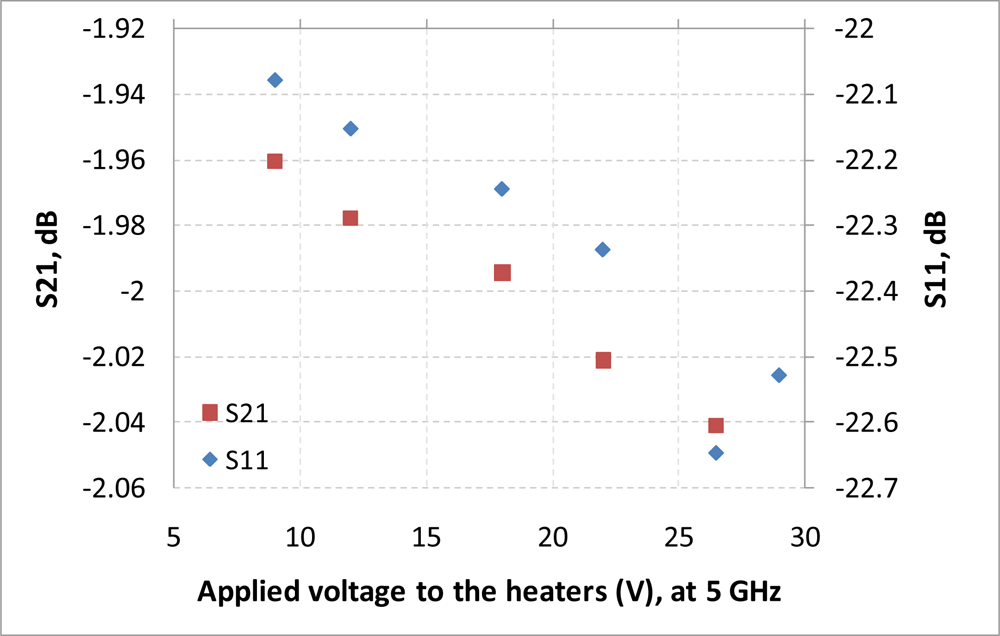
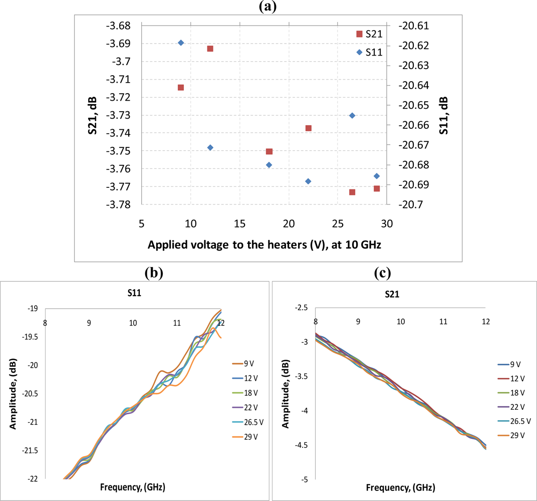
After performing simulations of temperature distributions of CPW due to localized heating, the device has been measured using a vector network analyzer (VNA) and a coplanar probe station. Before doing measurements, the probe station was calibrated using standard substrates. Applying voltages through the heaters, scattering parameters of the CPW have been recorded. Figures 6 and 7 display the measured results. It is seen that even for such small temperature variations predicted by the simulation in the last section, the reflection coefficient (S11) and transmission coefficient (S21) of the CPW have changed. The S11 has changed from −13.02 dB to −13.98 dB at 20 GHz when the voltage applied to the heaters has varied from 9 V to 29 V, which corresponds to the maximum temperature of the CPW ground line changing from around 306 K to 317 K. Under the same experiment conditions, S21 has changed from −6.22 dB to −6.01 dB. The relationships between measured scattering parameters and applied voltages to the heaters at 5 GHz, 10 GHz, 15 GHz, 20 GHz, 25 GHz, and 30 GHz are shown in Figures 8–13 respectively. As there is relatively large noise in the measurement compared to the signal level, average values (in the range of ±0.5 GHz) of S11 and S21 have been taken at above frequency points. It is shown from these figures, that reflection coefficient S11 has a decreasing trend with increasing temperatures except at 10 GHz (Figure 9 (a)). We have further investigated S parameters at around 10 GHz and found that it is very difficult to see how microwave performances vary against temperatures as the noise level is higher than the signal level (shown in Figure 9(b,c)). For S21, it decreases when the microwave signal at 5 GHz and 10 GHz (again the trend of S21 cannot be seen very clearly due to noise), and this trend has changed reversely when the microwave signal exceeds 15 GHz. It is seen that at 15 GHz, S21 decreases when voltages are below 15 V, and increases for voltages above 15 V. To further study microwave performance at this frequency, S21 in frequency range of 13 GHz to 17 GHz has been plotted in Figure 10(b), It is seen that the noise is too large compared to the signals, therefore the trend of S21 at around 15 GHz is not clear. In terms of amplitude of the scattering parameters, it shows that S11 increases linearly with increasing temperatures. At 5 GHz, the amplitude of S11 has changed by 2.1% when the applied voltage to the heaters has varied from 9 V to 29 V, and the amplitude of S21 has changed by 5.5%. For 15 GHz, the amplitude variation of S11 is 4.8%. When the microwave frequency is at 20 GHz, the S11 and S21 amplitudes have changed by 7.4% and 3.5%. While at 25 GHz, S11 and S21 amplitudes have changed by 6.9% and 2.8%. Finally at 30 GHz, the amplitudes of S11 and S21 have changed by 3.7% and 3.8%. For the current design, the temperature variations in the CPW structure are very small according to the heat transfer simulation in section 2. The temperature of the CPW cannot be further increased in this study, because the maximum temperature of the heaters almost reaches the point that causes thermal damage of the silicon. According to microwave theory, if the network has no loss and no gain, the output power must equal to input power, and so in this case |S11|2 + |S21|2 = 1. In order to find out the overall losses of the CPW versus temperatures, the losses (1 – |S11|2 − |S21|2) have been calculated and shown in Figure 14. It is seen from the Figure 14 that in low frequency range (0–14 GHz) losses increase with rising temperatures, and at high frequencies, losses decrease with rising temperatures.
4. Conclusions
Study of temperature effects on the RF performances of suspended CPW has been conducted using a test structure that consists of a suspended CPW and two symmetric spring-shaped silicon heaters adjacent to the CPW. Thermal transfer between the heaters and CPW has been simulated using FEM software, and the results show that although the maximum temperature of the silicon heaters is very high, the temperature of the CPW has not been much increased due to an air gap between heaters and CPW. Microwave measurements of the device have also been conducted, it is concluded that at low frequency band (<15 GHz), the scattering parameters have changed in much lower amplitude than at higher frequency band (>15 GHz). The experiments also show that S11 has a decreasing trend with increasing temperatures except at frequency point of 10 GHz, while S21 is reversely proportional to the temperature at lower frequency band, and becomes proportional to the temperature at higher frequency band. In the future, customized micromachining process will be selected in order to have the heaters directly in contact with the ground plane of the CPW, so that the effects on RF performances of the suspended CPW at much higher temperatures can be obtained.
Acknowledgments
The work is supported by the EPSRC, the Leverhulme Trust, and the Royal Society of UK.
References
- Facer, GR; Notterman, DA; Sohn, LL. Dielectric spectroscopy for bioanalysis: From 40 Hz to 26.5 GHz in a microfabricated wave guide. Appl. Phys. Lett 2001, 78, 996–998. [Google Scholar]
- Stuchly, SS; Bassey, CE. Microwave coplanar sensors for dielectric measurements. Meas. Sci. Technol 1998, 9, 1324–1329. [Google Scholar]
- Dragoman, M; Grenier, K; Dubuc, D; Bary, L; Plana, R; Fourn, E; Flahaut, E. Millimeter wave carbon nanotube gas sensor. J. Appl. Phys 2007, 101, 106103. [Google Scholar]
- Treizebre, A; Akalin, T; Bocquet, B. Planar excitation of Goubau transmission lines for THz bioMEMS. IEEE Microw. Wirel. Compon. Lett 2005, 15, 886–888. [Google Scholar]
- Wood, DK; Oh, SH; Lee, SH; Soh, HT; Cleland, AN. High-bandwidth radio frequency coulter counter. Appl. Phys. Lett 2005, 87, 184106. [Google Scholar]
- Li, L; Uttamchandani, D. Flip-chip distributed MEMS transmission lines (DMTLs) for biosensing applications. IEEE Trans. Ind. Electron 2009, 56, 986–990. [Google Scholar]
- Li, L; Uttamchandani, D. A microwave dielectric biosensor based on suspended distributed MEMS transmission lines. IEEE Sens. J 2009, 9, 1825–1830. [Google Scholar]
- Li, L. Simultaneous detection of organic and in-organic substances in a mixed aqueous solution using a microwave dielectric sensor. Prog. Electromagn. Res. C 2010, 14, 163–171. [Google Scholar]
- Lin, WY; Mao, JF; Shi, JL; Sun, XW. Performance degradation of some on-chip finite-ground coplanar waveguide (FGCPW) built passive devices at high temperature. Microw. Opt. Technol. Lett 2006, 48, 1754–1759. [Google Scholar]
- El Kaamouchi, M; Delatte, P; Si Moussa, M; Raskin, J-P; Vanhoenacker-Janvier, D. Temperature behaviour of spiral inductors on high resistivity substrate in SOI CMOS technology. Solid-State Electron 2008, 52, 1915–1923. [Google Scholar]
- Ponchark, GE; Jordan, JL; Scardelletti, MC. High temperature characteristics of coplanar waveguide on R-Plane sapphire and aluminium. IEEE Trans. Adv. Packag 2009, 32, 146–151. [Google Scholar]
- Moussa, MS; Pavageau, C; Lederer, D; Picheta, L; Danneville, F; Fel, N; Russat, J; Raskin, JP; Vanhoenacker-Janvier, D. Behaviour of TFMS and CPW line on SOI substrate versus high temperature for RF applications. Solid-State Electron 2006, 50, 1822–1827. [Google Scholar]
- Chow, LLW; Wang, Z; Jensen, BD; Saitou, K; Volakis, JL; Kurabayashi, K. Skin-effect self-heating in air suspended RF MEMS transmission-line structures. J. Microelectromech. Syst 2006, 15, 1622–1631. [Google Scholar]
- Shah, JJ; Sundaresan, SG; Geist, J; Reys, DR; Booth, JC; Rao, MV; Gaitan, M. Microwave dielectric heating of fluids in an integrated microfluidic device. J. Micromech. Microeng 2007, 17, 2224–2230. [Google Scholar]
- Li, L; Uttamchandani, D. Dynamic response modelling and characterization of a vertical electrothermal actuator. J. Micromech. Microeng 2009, 19, 075014. [Google Scholar]
- Johnstone, RW; Parameswaran, M. Modelling surface-micromachined electrothermal actuators. Can. J. Electr. Comput. Eng 2004, 29, 193–202. [Google Scholar]
- Huang, QA; Lee, NKS. Analysis and design of polysilicon thermal flexure actuator. J. Micromech. Microeng 1999, 9, 64–70. [Google Scholar]


| Parameter | Value | Unit |
|---|---|---|
| Thickness of structure | 20 | μm |
| Length of CPW | 4,000 | μm |
| Width of CPW ground line | 180 | μm |
| Width of CPW signal line | 200 | μm |
| Total length of heater | 2,000 | μm |
| Width of heater | 20 | μm |
| Air gap between heater and CPW ground line | 6 | μm |
| Air gap between ground line and signal line of CPW | 20 | μm |
| Resistivity of silicon | 5.6 × 10⁻⁶ | Ω-m |
| Temperature coefficient | 1 | 1/K |
| Ambient temperature | 300 | K |
| Thermal conductivity of silicon | 130 | W/(m*K) |
| Thermal conductivity of air | 0.03 | W/(m*K) |
| Convective heat transfer coefficient | 10 | W/(m3*K) |
| External temperature | 300 | K |
© 2011 by the authors; licensee MDPI, Basel, Switzerland. This article is an open access article distributed under the terms and conditions of the Creative Commons Attribution license (http://creativecommons.org/licenses/by/3.0/).
Share and Cite
Li, L.; Liu, Z. Study of Temperature Characteristics of Micromachined Suspended Coplanar Waveguides for Biosensing Applications. Sensors 2011, 11, 2640-2651. https://doi.org/10.3390/s110302640
Li L, Liu Z. Study of Temperature Characteristics of Micromachined Suspended Coplanar Waveguides for Biosensing Applications. Sensors. 2011; 11(3):2640-2651. https://doi.org/10.3390/s110302640
Chicago/Turabian StyleLi, Lijie, and Zhuming Liu. 2011. "Study of Temperature Characteristics of Micromachined Suspended Coplanar Waveguides for Biosensing Applications" Sensors 11, no. 3: 2640-2651. https://doi.org/10.3390/s110302640