BIPV-Powered Smart Windows Utilizing Photovoltaic and Electrochromic Devices

Abstract
: A BIPV-powered smart window comprising a building-integrated photovoltaic (BIPV) panel and an all-solid-state electrochromic (EC) stack is proposed. In the proposed device, the output voltage of the BIPV panel varies in accordance with the intensity of the incident light and is modulated in such a way as to generate the EC stack voltage required to maintain the indoor illuminance within a specified range. Two different EC stacks are fabricated and characterized, namely one stack comprising ITO/WO3/Ta2O5/ITO and one stack comprising ITO/WO3/lithium-polymer electrolyte/ITO. It is shown that of the two stacks, the ITO/WO3/lithium-polymer electrolyte/ITO stack has a larger absorptance (i.e., approximately 99% at a driving voltage of 3.5 V). The experimental results show that the smart window incorporating an ITO/WO3/lithium-polymer electrolyte/ITO stack with an electrolyte thickness of 1.0 μm provides an indoor illuminance range of 750–1,500 Lux under typical summertime conditions in Taiwan.1. Introduction
Many transition metal oxides have been investigated regarding their potential for use in electrochromic applications [1–16]. Among these oxides, tungsten oxide (WO3) is the most commonly used inorganic electrochromic compound due to its many favorable properties, including a high capacity for reversible Li+ insertion, a high coloration efficiency, good reversibility, relatively low price, and non-toxicity [3].
Smart windows, which change from transparent to frosted to opaque with the simple turn of a switch, provide a promising solution for controlling the amount of heat or light entering a building, and are invaluable in reducing heating, air-conditioning and lighting costs. Such windows generally incorporate an electrochromic (EC) stack comprising an active EC layer and a passive counter electrode sandwiched between two transparent electrical conductors (e.g., tin-doped indium oxide, ITO). Typically, the active EC layer consists of a thin glass plate coated with a thin film of WO3, NiO [4,5], V2O5 or MoO3 [6], while the counter electrode comprises a thin glass plate coated with lithium electrolyte [7] or some other form of anodically-colored transition metal oxide [8].
Ho et al. [1] presented a solid-state EC system comprising a WO3/Prussian blue (PB) thin film coupled with a proton-conducting, solid polymer electrolyte. It was shown that the device could be switched between a darkened state and a bleached state by applying electrical voltages of +1.2 V and −0.6 V, respectively. In the same year, Zhang et al. [2] proposed a smart window with a WO3/lithium-polymer electrolyte/V2O5 structure and showed that the transmittance of the device reduced from 74% to 12% within 60 s of switching the applied voltage from 1.8 V to −1.2 V. Later, Özer [3] used a sol-gel spin coating technique to coat glass slides with thin WO3 films prepared from a solution of tungsten oxychloride and tungsten complex precursor. The experimental results showed that the optical and electrochemical properties of the WO3 films exhibited electrochemical reversibility beyond 1,600 cycles with no change in performance. Maccari et al. [9] developed medium size (300 × 300 mm2) EC devices for architectural and automotive applications comprising WO3/vanadium pentoxide as the active electrode and a lithium-coated glass plate as the counter electrode.
Various deposition methods have been proposed for the preparation of thin WO3 films, including vacuum evaporation, electrochemical deposition, sol-gel deposition, chemical vapor deposition, spray pyrolysis, and sputtering [7,17–20]. Among these methods, magnetron sputtering has emerged to be of potential interest for production of wide-spread products due to its many favorable properties [7]. Kamal et al. [17] used an RF-sputtering technique to deposit amorphous WO3 films on glass substrates and found that the coloration of WO3 under the application of an external electrical field is the result of a hopping of the polarons within the film. Sivakumar et al. [18] deposited thin WO3 films on fluorine-doped tin oxide (FTO) coated glass slides using an electron beam evaporation technique with different substrate temperatures. The experimental results showed that the films deposited using a higher substrate temperature yielded a smaller modulation of the visible spectrum than those deposited at a lower temperature. Zhang et al. [20] fabricated self-organized macroporous WO3 films on ITO-coated glass slides via the anodic oxidation of DC-sputtered W layers. The anodized WO3 films were shown to have both a rapid switching speed (i.e., 8 s) and a large color contrast (i.e., 50%).
Smart windows are an effective means of reducing energy costs and achieving adjustable lighting levels for user comfort [21]. They vary the throughput of radiant energy and visible light by means of glass plates coated with a thin film having photochromic, thermochromic or electrochromic properties [22]. Lampert [23] examined various electrically-activated chromogenic glazings containing dispersed liquid crystals, dispersed particles and electrochromics, respectively. The results showed that transmittance ranges of 20–60%, 10–50% and 0.1–10% could be obtained with switching speeds of 100–200 ms given applied voltages ranging from 0–20 V to 150 V or more. Baloukas et al. [24] developed a smart window in which the single WO3 active layer within conventional devices was replaced by an EC interference filter comprising a stack of dense and porous WO3 layers. It was shown that the dense overlaying coating had no effect on the coloration of the underlying porous coating and a voltage switch of −0.6 V to +1.5 V was sufficient to prompt a change from a bleached state to a darkened state.
Building-integrated photovoltaics (BIPV) are finding increasing use in the construction of new buildings as either a primary or auxiliary source of electrical power. In the present study, a BIPV module is integrated with an EC stack in order to realize a BIPV-powered smart window. In the proposed device, the variable output voltage from the BIPV module is used to drive the EC stack and is modulated in such a way as to achieve the specified indoor illumination conditions. Two EC stacks are considered, namely one stack with an ITO/WO3/Ta2O5/ITO structure and a second stack with an ITO/WO3/lithium-polymer electrolyte/ITO structure. The diffraction pattern of the WO3 thin-film deposited on the ITO glass slide in each stack is examined using an X-Ray Diffraction (XRD) technique. The coloration and bleaching properties of the two stacks are examined under applied voltages of 3.5 V and 0 V, respectively. In addition, the transmittance and absorptance properties of the two stacks are analyzed and compared for driving voltages in the range of 0–3.5 V. Finally, an experimental investigation is performed to confirm the ability of the smart window to maintain appropriate indoor illumination conditions over the course of a typical sunny day in Taiwan.
2. Design
Figure 1 illustrates the smart window developed in this study. As shown, the window was designed for installation in the roof or dormer of a building, and comprises a BIPV panel, an EC stack and a controller. As the intensity of the solar irradiation on the BIPV panel increases, the output voltage from the BIPV module also increases. The output voltage is modulated by the controller and is then used to drive the EC stack in order to color the window.
As shown in Figure 1(b), the EC stack was sandwiched between two ITO-coated glass plates. ITO is a highly degenerated, wide-bandgap semiconductor material with relatively low resistivity and high transmittance in the visible region [25]. As a result, it is ideal for EC smart window applications. It was shown in [17] that the electrochromic effect in amorphous WO3 is due to the formation of tungsten bronze as a result of the double injection into the interstitial sites of the WO3 matrix of electrons from the active electrode and charge-compensating ions from the counter electrode. In other words, the formation of tungsten bronze occurs in accordance with the following process:
3. Fabrication
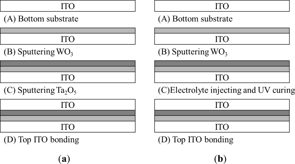
As shown in Figure 2, two EC stacks were fabricated in the current study, namely one stack with an ITO/WO3/Ta2O5/ITO structure and a second stack with an ITO/WO3/lithium-polymer electrolyte/ITO structure.
In both cases, the stacks were fabricated using ITO-coated glass slides with a thickness of 0.68 mm and dimensions of 150 × 150 mm2. The WO3 and Ta2O5 films were deposited on the glass slides using an RF magnetron sputtering system with W and Ta2O5 targets, respectively. In performing the sputtering process, the ITO substrates were positioned at a distance of 11.4 cm from the targets (99.99% purity), the gas pressure was maintained at 0.01 torr, and the RF power was set as 200 W. The deposition process was performed using mixtures of argon (50% and 80%) and pure oxygen (50% and 20%) for the W and Ta2O5 targets, respectively, as the reactive gas. Prior to deposition, the chamber was pumped to a background pressure of 10−6 torr for 1 h and a pre-sputtering process was performed for 10 min in order to remove any traces of impurities from the surface of the W target [26]. RF sputtering was then performed for 1.0 h, resulting in a WO3 film with a thickness of approximately 1,000 Å. For comparison purposes, one stack was fabricated using a sputtered layer of Ta2O5 (thickness: 3,000 Å) (see Figure 2(a)), while the other was fabricated using a solution of LiClO4, propylene carbonate and UV adhesive, which was cured using UV light to form an electrolyte layer with a thickness of 1.4 mm (see Figure 2(b)). ITO glass plates were bonded to the Ta2O5 and lithium-polymer layers, respectively, to realize the finished EC stacks. Finally, a BIPV panel with a thickness of 6.2 mm was attached to the upper ITO glass plate. The BIPV panel is a crystalline light-through module (ITRI, Taiwan). Its PMAX, VOC, ISC, VPMAX and IPMAX are 1.069 W, 3.757 V, 0.412 V, 2.902 V and 0.368 A, respectively.
4. Results and Discussion
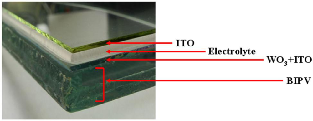
Figure 3 presents a photograph of the integrated BIPV panel/EC stack. The diffraction pattern of the WO3 thin-film deposited on the ITO glass slide was observed using an XRD measurement system (XRD-600 LabX, Shimadzu, Japan). The transmittance and absorptance properties of the two stacks were then investigated under various applied voltages in the range of 0–3.5 V. The illuminance of the light transmitted through the BIPV panel was measured over the period of 8:00 am to 4:00 pm on a summer day with natural light incident directly upon the panel. A controller was then designed to modulate the output voltage of the BIPV panel in such a way as to generate a suitable input voltage for the EC stack. Finally, the indoor illuminance provided by the smart window/controller under sunny daytime conditions was measured over the period of 8:00 am to 4:00 pm.
4.1. Diffraction Pattern of WO3 Thin-Film on ITO Glass Slide
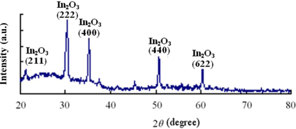
Figure 4 shows the diffraction pattern of the WO3 thin-film deposited on the ITO glass slide. It is seen that apart from five distinct peaks corresponding to the ITO underlayer, the diffraction pattern is relatively featureless; indicating that the WO3 film has poor crystallinity.
4.2. Observations of Coloration and Bleaching
The coloration and bleaching behaviors of the EC stacks were observed under various voltages in the range of 0–3.5 V. It was found that for both stacks, a coloration state was induced at an applied voltage of +3.5 V in 15–20 s, while a beached state was induced at an applied voltage of 0 V in the same response time range (see Figure 5).
4.3. Effect of Applied Electrical Voltage on Transmittance and Absorptance Properties of EC Stacks
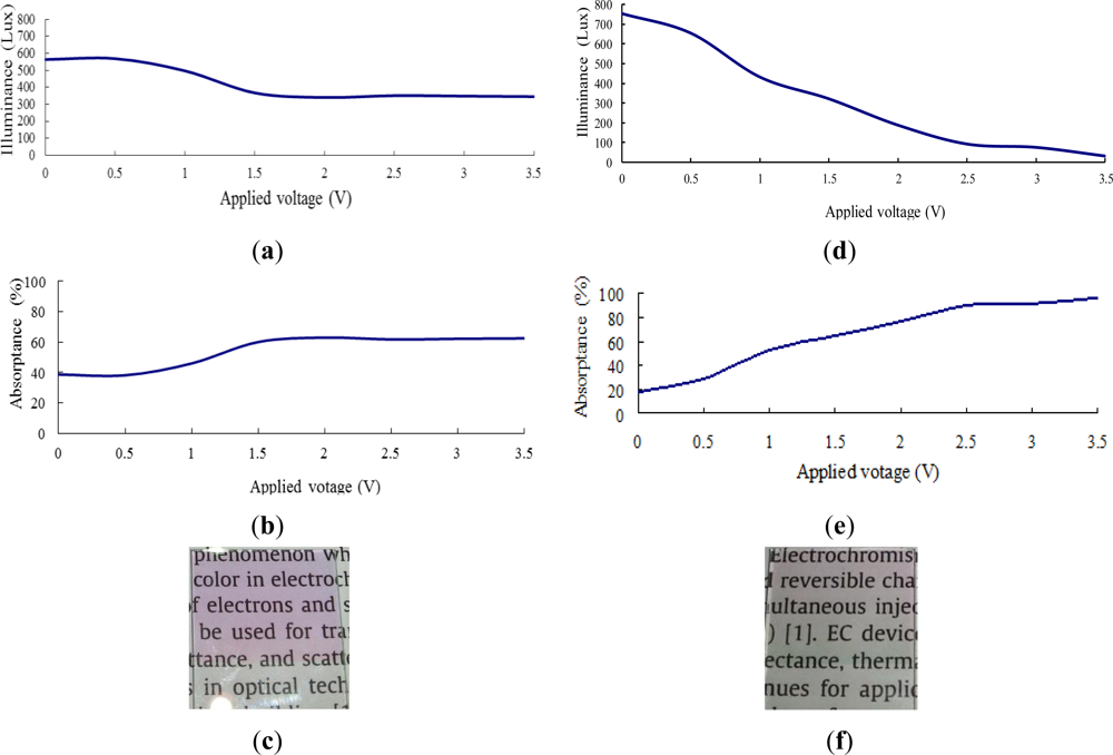
Figure 6 shows the transmittance and absorptance behaviors of the ITO/WO3/Ta2O5/ITO EC stack given an incident illuminance of 900 Lux and applied voltages in the range of 0–3.5 V. Note that in Figure 6(a–c), the Ta2O5 film has a thickness of 375 nm, while in Figure 6(d–f), the Ta2O5 film has a thickness of 750 nm. As shown in Figure 6(a), the indoor illuminance gradually reduces as the voltage is increased to 1.5 V. However, as the voltage is further increased to 3.5 V, the illuminance remains approximately constant at around 400 Lux. In other words, 1.5 V represents a saturation voltage, above which the number of ions transferred from the Ta2O5 layer remains approximately the same. An inspection of Figure 6(b) shows that the maximum absorptance of the EC stack is around 60%. As shown in Figure 6(d), the illuminance of the transmitted light falls rapidly with an increasing voltage due to the stronger ion movement to the WO3 layer when the thickness of the Ta2O5 film is increased to 750 nm. Thus, given the maximum applied voltage of 3.5 V, the illuminance of the transmitted light is less than 100 Lux. From Figure 6(e), the corresponding absorptance is found to be around 95%. Overall, the results presented in Figure 6(d,e) show that as the thickness of the Ta2O5 film is increased, the number of charge-compensating ions provided by the Ta2O5 film also increases, and thus a greater absorptance is obtained. Figure 6(c,f) illustrate the transparency of the two EC devices in the fully-bleached state given an applied voltage of 0 V. It is observed that a good transparency is obtained even given a Ta2O5 film thickness of 750 nm.
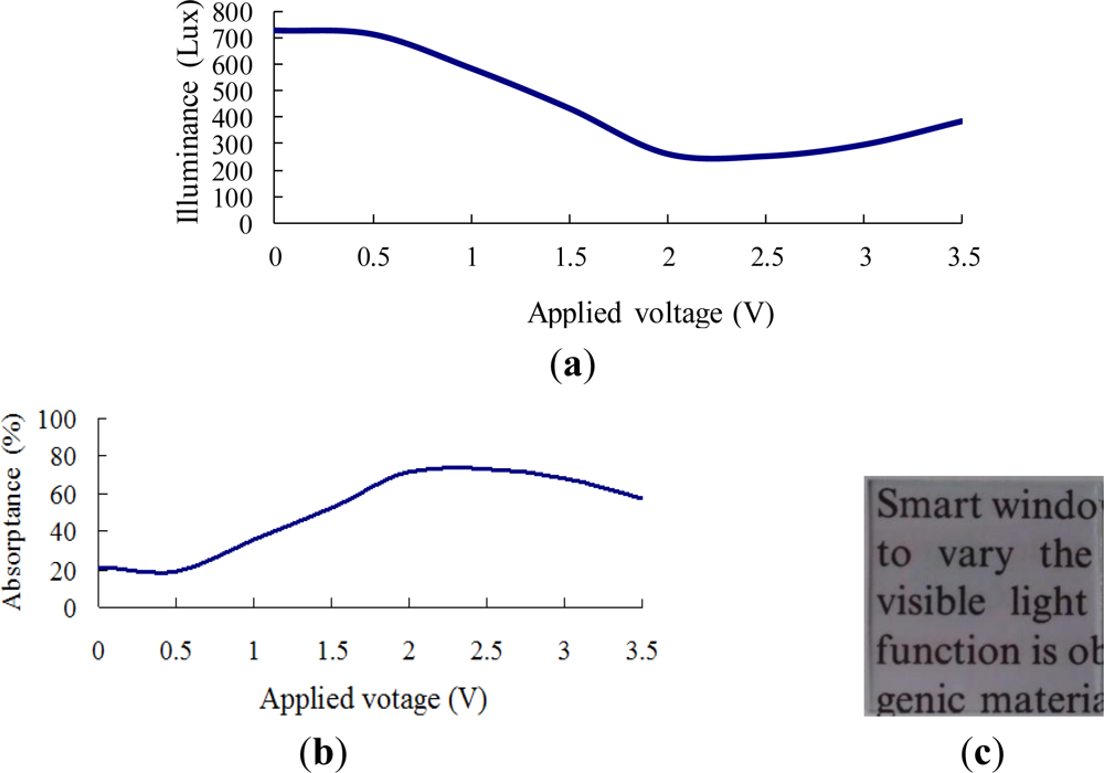
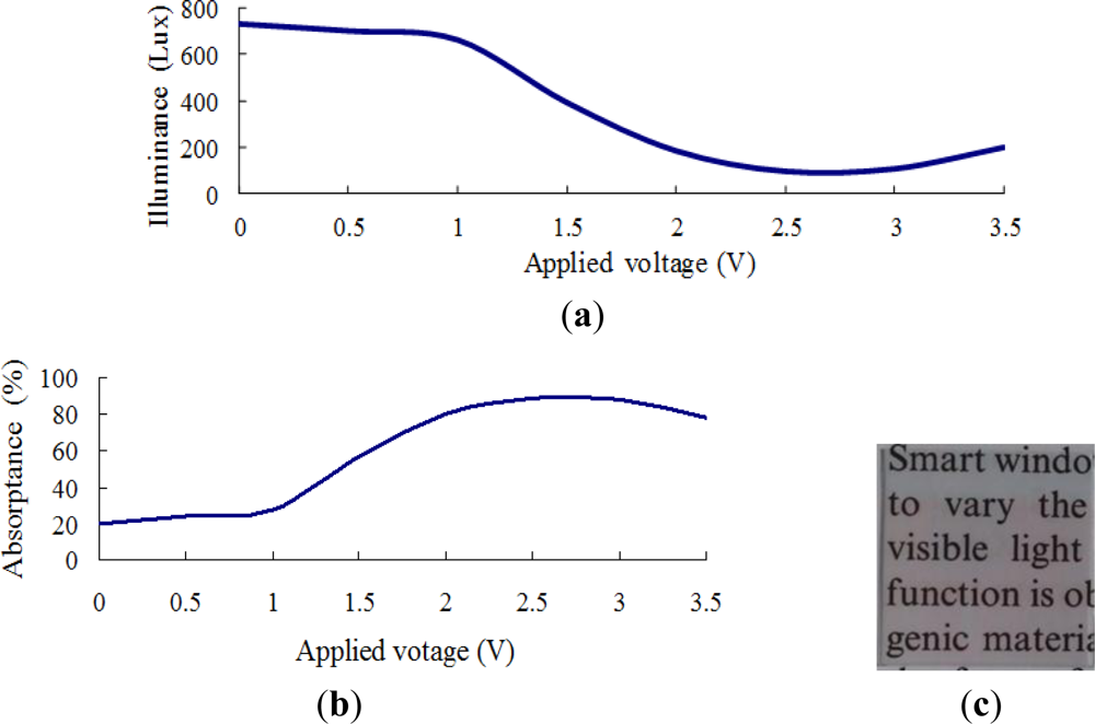
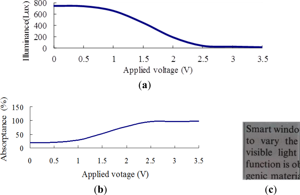
Figures 7–10 show the transmittance and absorptance behaviors of the ITO/WO3/lithium-polymer electrolyte/ITO stack given applied voltages of 0–3.5 V and electrolyte film thicknesses of 250, 500, 750 and 1,000 nm. Note that the illuminance of the incident light is 900 Lux in all cases. Figure 7(a) shows that the illuminance of the transmitted light decreases as the applied voltage is increased to 2 V, but then increases slightly as the voltage is increased further due to an insufficient supply of charge-compensating ions from the thin (250 nm) electrolyte film. A similar tendency is observed in the EC stack with an electrolyte thickness of 500 nm (Figure 8(a)). However, for the EC stacks with an electrolyte thickness greater than 500 nm, the illuminance of the transmitted light saturates at an applied voltage of approximately 2.5 V (Figures 9(a) and 10(a)). The corresponding absorptance is found to be approximately 99% (Figures 9(b) and 10(b)). Figures 7(c), 8(c), 9(c) and 10(c) illustrate the transparency properties of the four EC stacks. It is seen that a good transparency is maintained even for an electrolyte layer with a thickness of 1000 nm.
Comparing Figures 6 and 7–10, it is seen that the EC stack with a lithium-polymer electrolyte yields a better absorptance performance under the maximum applied voltage (approximately 99%) than the EC stack with a Ta2O5 film (95%) due to the difference of their ion conductivity. Thus, the ITO/WO3//lithium-polymer electrolyte/ITO stack with an electrolyte thickness of 1,000 nm was chosen for integration with the BIPV panel to form the BIPV-powered smart window.
4.4. Modulation of Indoor Illuminance
Figure 11 shows the variation in the illuminance of the light incident on the BIPV panel over the period of 8:00 am to 4:00 pm on a typical summer day in Taiwan with the natural light incident directly on the smart window. It is seen that an illuminance of more than 70,000 Lux is obtained at midday. This value is far higher than the recommended indoor illuminance range of 750–1,500 Lux during daytime hours [27]. Thus, a significant reduction in the indoor illuminance is required.
To optimize the indoor illuminance during the daytime hours, it is necessary to modulate the absorptance of the EC stack in accordance with changes in the intensity of the solar irradiation on the BIPV panel of the smart window. The results presented in Section 4.3 have shown that the absorptance of the ITO/WO3/lithium-polymer electrolyte/ITO stack increases with an increasing driving voltage. Meanwhile, the results presented in Section 4.4 have shown that the illuminance of the light transmitted through the BIPV module increases as the intensity of the solar irradiation increases. In other words, to maintain an acceptable indoor illuminance condition, the absorptance of the EC stack should be increased as the outdoor illuminance increases. For a photovoltaic device such as a BIPV panel, the output voltage increases as the illuminance of the incident light on the panel increases. Thus, in the present study, the output voltage from the BIPV panel is modulated adaptively in order to generate the EC driving voltage required to maintain the optimal indoor illuminance conditions given changes in the intensity of the outdoor solar irradiation. Figure 12(a) illustrates the layout of the control circuit used to modulate the BIPV output voltage. The ITO/WO3/lithium-polymer electrolyte/ITO EC stack has an operating current of 20 mA and an internal resistance of 120 Ω. Thus, the controller was implemented using a series connection of one 40 Ω of resistor; causing the output voltage of the BIPV panel to be divided with a 75% ratio for optimizing the input voltage of the EC device. Figure 12(b) shows the variations of the original and modulated voltages from the BIPV module over the period of 8:00 am to 4:00 pm. The modulated voltage can control the absorptance effect with an optimization ratio following the experimental results of Figure 10(b).
Figure 13 shows the variation of the original transmitted sunlight intensity through the smart window over the period of 8:00 am to 4:00 pm (Figure 13(upper)) and the corresponding variation of the indoor illuminance, as controlled by the smart window (Figure 13(lower)). It can be seen that the smart window ensures that the indoor illuminance remains within the recommended range of 750–1,500 Lux from 8.40 to 15.40 despite significant changes in the outdoor solar irradiation intensity.
5. Conclusions
This study has fabricated and characterized a BIPV-powered smart window comprising a BIPV panel and an EC stack for optimizing the indoor illuminance conditions without the need for shading devices. The novelty of the study is that the output voltage of the BIPV panel varies in accordance with the intensity of the incident light and can be modulated in such a way to generate the EC stack voltage required to maintain the indoor illuminance within a specified range without any requirement of external energy source. Two all-solid-state EC stacks have been fabricated, namely one stack with an ITO/WO3/Ta2O5/ITO structure and one stack with an ITO/WO3/lithium-polymer electrolyte/ITO structure. The experimental results have shown that the latter stack yields a larger absorptance (approximately 99%) given the maximum driving voltage of 3.5 V. A control scheme has been proposed for modifying the output voltage of the BIPV panel in such a way as to optimize the absorptance of the ITO/WO3/lithium-polymer electrolyte/ITO stack in response to changes in the outdoor solar illuminance. Though ITO is an ideal solution for the utilization of the EC-based smart windows, the scarcity of its main component (In) should be noticed and its replacement component is hoped to be found in the field of materials science and engineering for the universalization of the EC-based smart windows. In the paper, it has been shown that the smart window ensures that the indoor illuminance remains within the recommended range of 750–1,500 Lux despite significant changes in the intensity of the outdoor solar irradiation.
Acknowledgments
The authors would like to thank Chia-Yen Lee in the Department of Vehicle Engineering, National Pingtung University of Science and Technology, Taiwan, for providing the BIPV panels and suggestions on the deposition technology.
References
- Ho, K.C.; Rukavina, T.G.; Greenberg, C.B. Tungsten oxide-prussian blue electrochromic system based on a proton-conducting polymer electrolyte. J. Electrochem. Soc 1994, 141, 2061–2067. [Google Scholar]
- Zhang, J.G.; Benson, D.K.; Tracy, C.E.; Deb, S.K.; Czanderna, A.W.; Crandall, R.S. Optimization study of solid-state electrochromic devices based on WO3/lithium-polymer electrolyte/V2O5 structures. J. Electrochem. Soc 1994, 141, 2795–2800. [Google Scholar]
- Özer, N. Optical and electrochemical characteristics of sol-gel deposited tungsten oxide films: A comparison. Thin Solid Films 1997, 304, 310–314. [Google Scholar]
- Iwata, E.; Mikage, K.; Sakaguchi, H.; Kitao, M.; Sasaki, A. Nanometer scale-electrochromic modification of NiO films using a novel technique of scanning near-field optical microscopy. Solid State Ion 2003, 163, 7–13. [Google Scholar]
- Park, S.H.; Lim, J.W.; Yoo, S.J.; Cha, I.Y.; Sung, Y.E. The improving electrochromic performance of nickel oxide film using aqueous N,N-dimethylaminoethanol solution. Sol. Energ. Mater. Sol. Cell 2011. [Google Scholar] [CrossRef]
- Mahajan, S.S.; Mujawar, S.H.; Shinde, P.S.; Inamdar, A.I.; Patil, P.S. Structural, morphological, optical and electrochromic properties of Ti-doped MoO3 thin films. Sol. Energ. Mater. Sol. Cell 2011, 93, 183–187. [Google Scholar]
- Zelazowska, E.; Rysiakiewicz-Pasek, E. WO3-based electrochromic system with hybrid organic-inorganic gel electrolytes. J. Non Cryst. Solids 2008, 354, 4500–4505. [Google Scholar]
- Passerini, S.; Scrosati, B. Characterization of nonstoichiometric nickel oxide thin-film electrodes. J. Electrochem. Soc 1994, 141, 889–894. [Google Scholar]
- Maccari, A.; Macrelli, G.; Polato, P.; Poli, E. Design, production and chracterisation of an all solid state electrochromic medium size device. Sol. Energ 1998, 63, 217–229. [Google Scholar]
- Granqvist, C.G. Electrochromic tungsten oxide films: Review of progress 1993–1998. Sol. Energ. Mater. Sol. Cell 2000, 60, 201–262. [Google Scholar]
- Wu, J.J.; Hsieh, M.D.; Liao, W.P.; We, W.T.; Chen, J.S. Fast-switching photovoltachromic cells with tunable transmittance. ACS Nano 2009, 3, 2297–2303. [Google Scholar]
- Huang, H.; Lu, S.X.; Zhang, W.K.; Gan, Y.P.; Wang, C.T.; Yu, L.; Tao, X.Y. Photoelectrochromic properties of NiO film deposited on an N-doped TiO2 photocatalytical layer. J. Phys. Chem. Solids 2009, 70, 745–749. [Google Scholar]
- Huang, H.; Jiang, L.; Zhang, W.K.; Gan, Y.P.; Tao, X.Y.; Chen, H.F. Photoelectrochromic properties and energy storage of TiO2−xNx/NiO bilayer thin films. Sol. Energ. Mater. Sol. Cell 2010, 94, 355–359. [Google Scholar]
- Leftheriotis, G.; Syrrokostas, G.; Yianoulis, P. Development of photoelectrochromic devices for dynamic solar control in buildings. Sol. Energ. Mater. Sol. Cell 2010, 94, 2304–2313. [Google Scholar]
- De Filpo, G.; Mormile, S.; Nicoletta, F.P.; Chidichimo, G. Fast, self-supplied, all-solid photoelectrochromic film. J. Power Sources 2010, 195, 4365–4369. [Google Scholar]
- Leftheriotis, G.; Syrrokostas, G.; Yianoulis, P. “Partly covered” photoelectrochromic devices with enhanced coloration speed and efficiency. Sol. Energ. Mater. Sol. Cell 2012, 96, 89–92. [Google Scholar]
- Kamal, H.; Akl, A.A.; Abdel-Hady, K. Influence of proton insertion on the conductivity, structural and optical properties of amorphous and crystalline electrochromic WO3 films. Phys. B 2004, 349, 192–205. [Google Scholar]
- Sivakumar, R.; Gopalakrishnan, R.; Jayachandran, M.; Sanjeeviraja, C. Investigation of X-ray photoelectron spectroscopic (XPS), cyclic voltammetric analysis of WO3 films and their electrochromic response in FTO/WO3/electrolyte/FTO cells. Smart Mater. Struct 2006, 15, 877–888. [Google Scholar]
- Ak, M.; Ak, M.S.; Güllü, M.; Toppare, L. Optoelectrochemical properties of poly(5,12-dihydrothieno [3′,4′:2,3] [1,4] dioxocino [6,7-b] quinoxaline-co-2,2′ bithiophene) and its electrochromic device application. Smart Mater. Struct 2007, 16, 2621–2626. [Google Scholar]
- Zhang, J.; Wang, X.L.; Xia, J.H.; Gu, C.D.; Zhao, Z.J.; Tu, J.P. Enhanced electrochromic performance of macroporous WO3 films formed by anodic oxidation of DC-sputtered tungsten layers. Electrochim. Acta 2010, 55, 6953–6958. [Google Scholar]
- Lee, E.S.; Selkowitz, S.E.; Clear, R.D.; DiBartolomeo, D.L.; Klems, J.H.; Fernandes, L.L.; Ward, G.J.; Inkarojrit, V.; Yazdanian, M. Advancement of Electrochromic Window; California Energy Commission: Sacramento, CA, USA, 2006. [Google Scholar]
- Granqvist, C.G.; Azens, A.; Hjelm, A.; Kullman, L.; Niklasson, G.A.; Rönnow, D.; Strømme Mattsson, M.; Veszelei, M.; Vaicars, G. Recent advances in electrochromics for smart windows applications. Sol. Energ 1998, 63, 199–216. [Google Scholar]
- Lampert, C.M. Smart switchable glazing for solar energy and daylight control. Sol. Energ. Mater. Sol. Cell 1998, 52, 207–221. [Google Scholar]
- Baloukas, B.; Lamarre, J.M.; Martinu, L. Electrochromic interference filters fabricated from dense and porous tungsten oxide films. Sol. Energ. Mater. Sol. Cell 2011, 95, 807–815. [Google Scholar]
- You, D.J.; Choi, S.K.; Han, H.S.; Lee, J.S.; Lim, C.B. Effect of the deposition geometry on the electrical properties within tin-doped indium oxide film deposited under a given RF magnetron sputtering condition. Thin Solid Films 2001, 401, 229–234. [Google Scholar]
- Ke, M.T.; Lee, M.T.; Lee, C.Y.; Fu, L.M. A MEMs-based benzene gas sensor with a self-heating WO3 sensing layer. Sensors 2009, 9, 2895–2906. [Google Scholar]
- Ho, M.C.; Chiang, C.M.; Chou, P.C.; Chang, K.F.; Lee, C.Y. Optimal sun-shading design for enhanced daylight illumination of subtropical classrooms. Energ. Build 2008, 40, 1844–1855. [Google Scholar]


© 2012 by the authors; licensee MDPI, Basel, Switzerland This article is an open access article distributed under the terms and conditions of the Creative Commons Attribution license (http://creativecommons.org/licenses/by/3.0/).
Share and Cite
Ma, R.-H.; Chen, Y.-C. BIPV-Powered Smart Windows Utilizing Photovoltaic and Electrochromic Devices. Sensors 2012, 12, 359-372. https://doi.org/10.3390/s120100359
Ma R-H, Chen Y-C. BIPV-Powered Smart Windows Utilizing Photovoltaic and Electrochromic Devices. Sensors. 2012; 12(1):359-372. https://doi.org/10.3390/s120100359
Chicago/Turabian StyleMa, Rong-Hua, and Yu-Chia Chen. 2012. "BIPV-Powered Smart Windows Utilizing Photovoltaic and Electrochromic Devices" Sensors 12, no. 1: 359-372. https://doi.org/10.3390/s120100359