CMOS-MEMS Test-Key for Extracting Wafer-Level Mechanical Properties


Abstract
: This paper develops the technologies of mechanical characterization of CMOS-MEMS devices, and presents a robust algorithm for extracting mechanical properties, such as Young’s modulus, and mean stress, through the external electrical circuit behavior of the micro test-key. An approximate analytical solution for the pull-in voltage of bridge-type test-key subjected to electrostatic load and initial stress is derived based on Euler’s beam model and the minimum energy method. Then one can use the aforesaid closed form solution of the pull-in voltage to extract the Young’s modulus and mean stress of the test structures. The test cases include the test-key fabricated by a TSMC 0.18 μm standard CMOS process, and the experimental results refer to Osterberg’s work on the pull-in voltage of single crystal silicone microbridges. The extracted material properties calculated by the present algorithm are valid. Besides, this paper also analyzes the robustness of this algorithm regarding the dimension effects of test-keys. This mechanical properties extracting method is expected to be applicable to the wafer-level testing in micro-device manufacture and compatible with the wafer-level testing in IC industry since the test process is non-destructive.1. Introduction
Due to the excellent development of the complementary metal oxide semiconductor (CMOS) technology, many micro-electromechanical systems (MEMS) devices such as comb-fingers [1], micro-mirrors [2], and resonators [3], the so-called CMOS-MEMS, can be fabricated by standard CMOS processes. The main advantage of CMOS-MEMS is batch production. Apart from the electrical testing of circuits, the MEMS-side still requires the mechanical testing of micro-sensing or -actuating components. However, there is no standard mechanical testing method for CMOS-MEMS devices. Characterization of the mechanical properties of CMOS-MEMS devices is important since their performance depends on the constitutive properties of the thin film made by the CMOS process. It is known that the properties of thin films are different from those of bulk materials, depending on the fabrication process. Moreover, large residual stress may induce failure of the micro-devices and circuits. Therefore, the material properties, such as Young’s modulus and residual stress, should be controlled as early as possible to ensure the repeatability for each device.
The property-extraction methods for large-scale implementation in MEMS fabrication require additional measurement and actuation equipment or complicated test structure designs. These methods are not compatible with IC metrology technologies. From the mechanical viewpoint of MEMS devices, the important thin-film material parameters are Young’s modulus [4–15], residual stress [7,9,15–18], Poisson’s ratio and shear modulus [15], residual strain [8,19], and hardness [20]. Among these mentioned parameters, Young’s modulus and residual stress have attracted the most attention. By using appropriate actuation and measurement techniques, these material properties can be extracted by determining the deformation or dynamic response of the test microstructures subjected to given external loads. Table 1 summarizes six different actuation methods and eight different measurement methods for extracting material properties in MEMS devices.
The electrostatic method employs a bias voltage to deflect the microtest structure downward to the ground plane [4,5,8,21]. The vibration method adopts comb drivers, piezoelectric shakers, or acoustic waves to vibrate the microtest structure [6,22]. Pulsed laser light can also be used to excite micro beams [23,24]. The force/pressure method uses the probe of atomic force microscope(AFM) or a nanoindenter to apply a force on the micro test structure or apply barometric pressure on the test membrane [12,13]. The thermal method heats the test structure to deform it [15], yet the heating time, and the uniform temperature field are critical issues in this testing method. The pre-deformation method does not need any actuation as it makes use of the deformation induced by large initial stresses [16,17,19,25]. In [16] the detection film on a cantilever beam firstneeds to be deposited, and then the variance of curvature is observedto determine the residual stress. Interferometers are a very common apparatus for measuring deformations or vibrations. For example, in some literatures [4–6] the optical signal or dynamic response is detected to extract the mechanical properties of test structures. These methods are manual, and need operators to judge the output signal. AFMs and scanning electron microscopes (SEMs) can also be used to measure the deformation. In [18] the difference of test beam length due to the residual stress effect is measured, but the detection signal is too small to identify the strain, therefore a specific apparatus is needed to enlarge the output signal. In some literature X-Ray diffraction (XRD) is used to measure the indentation imprint [14,20]. The pull-in method detects the pull-in voltage of micro test structures [9,26,27]. Besides, a micro tensile test [10] is used to determine the Young’s modulus, but the test samples need to be fabricated in specific shape to fit the clamping apparatus of the tensile tester. Nanoindenters [28] are also a common technique for extracting Young’s modulus and hardness of thin films. Nevertheless, this method can’t extract the residual stress of thin films. The modified Stoney’s equation (Equation (1)) [29] to evaluate the film stress is proposed as follows:
2. Electromechanical Behavior of the CMOS-MEMS Bridge Test-key
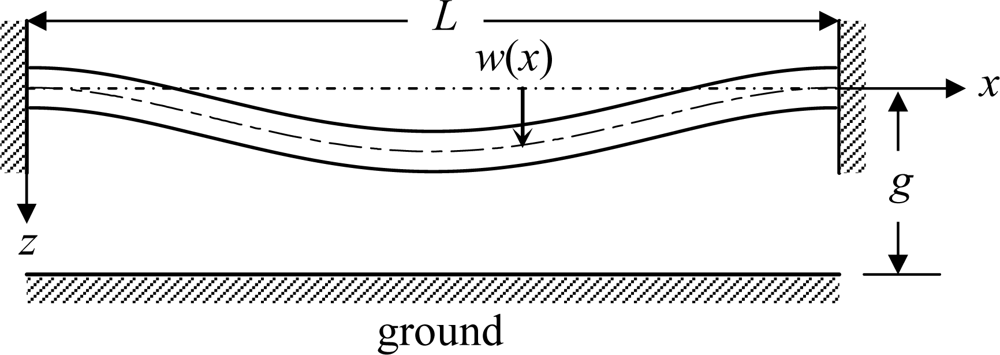
A conceptual diagram of a micro bridge is shown in Figure 1. The beam is of length L, width b, thickness h, and is separated from the ground by an initial gap g. As actuated by a constant drive voltage V, the electrostatic force causes a position-dependent deflection w(x). The following assumptions are made to simulate the bridge:
The bridge is homogeneous and with uniform cross section.
The bridge is within the Euler-Bernoulli model.
The stress gradient is neglected.
Small deflection and ideal fixed boundary conditions.
2.1. Energy Expression
The mechanical strain energy of an infinitesimal beam element is:
The total mechanical strain energy of the beam, as shown in Figure 1, can be expressed as:
It should be mentioned that nonlinearities are simplified with only in the electrostatic part of the model. Indeed, the beam structure is assumed linearly elastic, without any consideration of geometrical nonlinearity in virtue of large deformation. Expanding the electrostatic terms in Equation (6) by Taylor’s series with respect to the initial equilibrium position, i.e., w = 0, and truncate the fifth and higher order terms since (w/g)n << 1 for n≥5. Therefore, the total system potential energy U becomes:
2.2. Approximate Analytical Solution to Pull-in Voltage
The exact solution for the electrostatic-actuated beam is difficult to obtain since it is a nonlinear system with the nonlinear electrostatic force coupled with the structural deflection. Thus, such problem is often solved by the approximate analytical solution. Using the assumed mode method [38], the deflection function w(x) is expressed as:
Substituting Equations (8) and (9) into Equation (7) yields:
The system is in static equilibrium when the first-order derivative of the total potential energy U with respect to the coefficient η equals zero, i.e., dU/dη = 0, then one have:
The coefficients cj depend only on the geometrical parameters of beam. Whether the equilibrium is stable or unstable is determined by the second-order derivative of the total potential energy with respect to η. At the transition from a stable to an unstable equilibrium, the second-order derivatives of the total potential energy with respect to η also equals zero, i.e., d2U/dη2 = 0, then one has:
Substituting Equation (14) into Equation (12) gives:
Equation (15) is a cubic equation of η and can be solved by Cardan solution[39]. The real number root of Equation (15) gives rise to the coefficient ηPI at pull-in as:
Substituting Equation (16) into Equation (14) gives the approximate analytical solution to the pull-in voltage VPI as:
As shown in Equation (17), the pull-in voltage contains two terms, the first one is dependent on initial residual stress, and the second one is dependent on beam flexibility. The pull-in voltage increases as the increasing of initial stress (σ0) or Young’s modulus (E). A beam is considered as wide beam as b/h≥ 5. Wide beams exhibit plane strain conditions; therefore, the Young’s modulus (E) should be replaced by the equivalent Young’s modulus Ẽ = E/(1 –ν2) and the residual stress (σ0) should be replaced by the equivalent residual stress σ̃0= σ0(1 –ν2). Therefore, Equation (17) yields:
3. Wafer-Level Mechanical Properties Extracting
3.1. Algorithm
The correlation between the pull-in voltage and the material parameters must be formulated quantitatively to realize the idea of extracting mechanical properties from pull-in voltage of the test beam. An equilibrium equation has been derived based on Euler-Bernoulli beam model and the fringing filed capacitance model. The equilibrium equation, Equation (18) yields:
For a given beam with the pull-in voltage VPI, there are two unknowns in Equation (19), i.e., σ̃0 and Ẽ. Therefore, one needs two test beams with different length to get the two unknowns. For the two test beams made of the same material, but with different length, they have the same Young’s modulus and mean stress but different pull-in voltages and different S and B parameters. Then, one has two equations:
By rearranging Equation (22), the mean stress (σ̃0) and Young’s modulus (Ẽ) are given as the following matrix operational form:
One can extract Young’s modulus (Ẽ) and mean stress (σ̃0) easily by substituting the measured pull-in voltages of the two test beams with different length into Equation (23).
3.2. Algorithm Verification
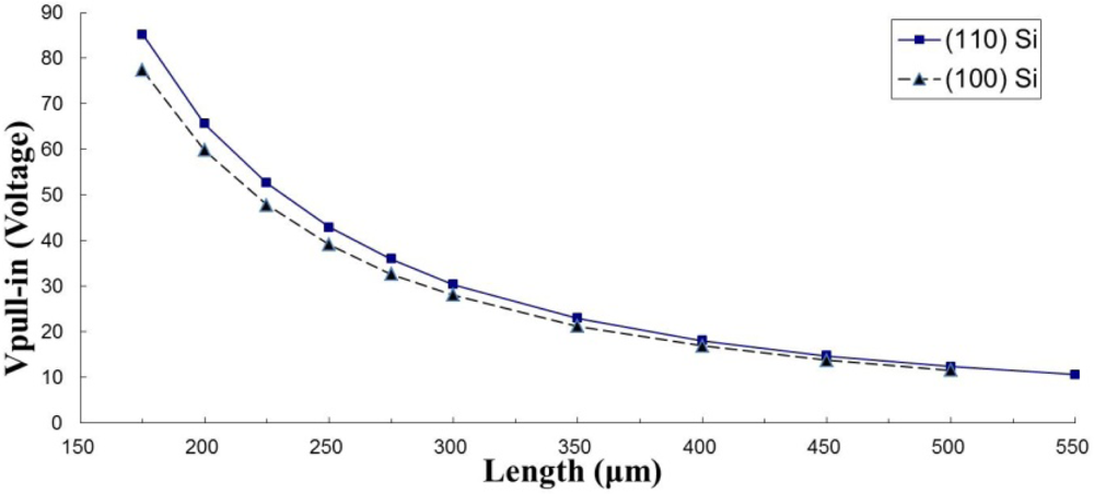
Osterberg [9] had measured pull-in voltages of numerous fixed-fixed beams with different lengths. The authors selected Osterberg’s measured data of two arbitrary test beams and substituted them into the algorithm to verify the validity of the present method. Table 2 lists the geometrical parameters and pull-in voltages of the selected fixed-fixed beams which are made of mono-crystalline silicon. There are two groups of fixed-fixed beams listed in Table 2; each group contains six beams of different lengths. The difference of the two groups is only the crystalline plane of cross section. The first group is in the (100) crystalline plane while the second one is in the (110) crystalline plane. The author selected two beams from each group and substituted the measured data and beam dimensions into Equation (23) to extract Young’s modulus (Ẽ) and mean stress (σ̃0). Note that the cross-section of the beams of group 1 are in the (100) crystalline plane while that of the group 2 are in the (110) crystalline plane. The Young’s modulus of mono-crystalline silicon in (100) and (110) are 138 GPa and 168 GPa, respectively. The mean stresses of the two beam-samples are 10 MPa [9].
Tables 3 and 4 list the extracted Young’s modulus (Ẽ) and mean stress (σ̃0) of mono-crystalline silicon in (100) and (110), respectively. It is shown that the extracted values of the present algorithm agree well with the average extracted value of Osterberg’s results [9], but with better convergence than Osterberg’s algorithm. The variety of standard deviation VSD of the extracted Young’s modulus (Ẽ) are all within 1% which are almost tenth of the deviations of Osterberg’s results [9] for both mono-crystalline silicon in (100) and (110). Besides, the VSD of the extracted mean stress (σ̃0) are all within 2%, which are also almost tenth of the deviations of Osterberg’s results [9] for both mono-crystalline silicon in (100) and (110).
4. Experimental Methodology
4.1. Sample Preparation
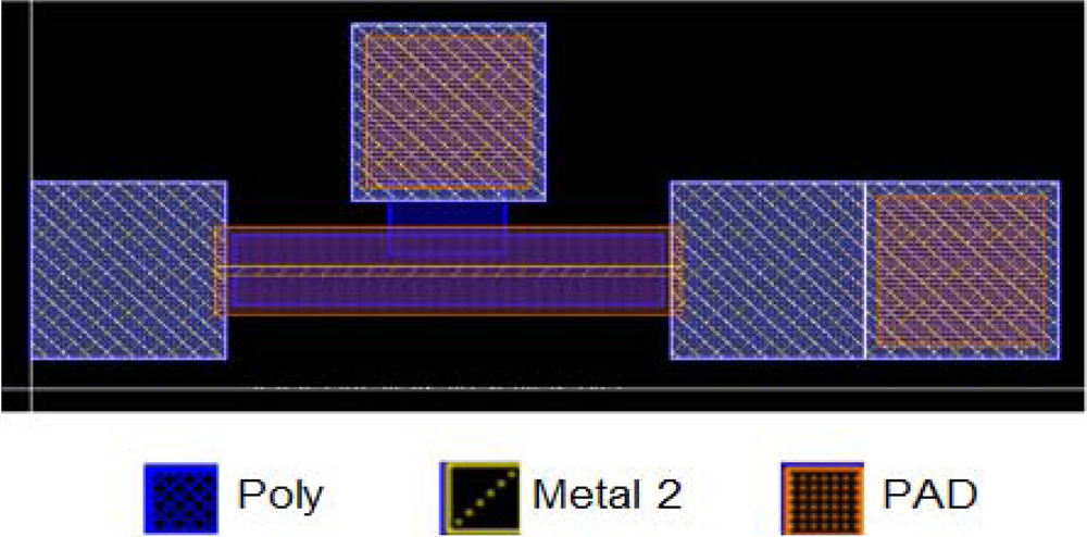
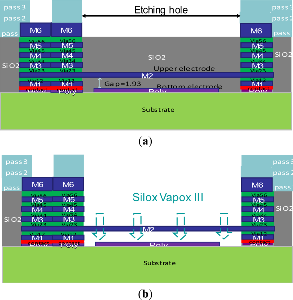
This paper takes bridge-type structures as test structures. The test structures are fabricated by a TSMC 0.18 μm 1P6M standard CMOS process. The upper electrode is metal 2, and the bottom electrode is a poly layer. The anchors are composed of metal and poly layers where viasconnect columns between each metal layer, and contact is the connecting column between metal 1 and the poly layer. When a driving voltage is applied between the test structure and ground plane, the test structure will deflect downward to the ground and this results in a capacitance variation. Figure 2 reveals the layout of the bridge-type test-key. There are two places which are defined as PAD layers-probing pad location and etching hole. The defined area of PAD layer at anchors is the probing pad location. It should be noticed that the probing location must maintain an appropriate distance away from the test structure to avoid measurement uncertainty. The other defined area of PAD layer between the neighboring passivation layers is the etching hole which makes the sacrificial layer etched by etching solution and then results in the structure release. Since the anchors are composed of metal layer, poly layers, via and contact columns, it can reduce the under-cut effect compared to the anchors composed of metal and poly layer without via and contact columns between that when the structures are soaked in etching solution.
Figure 3 shows the schematic cross-section of the bridge-type test-key after the CMOS process and after post-process. A silicon dioxide layer between the upper electrode and the bottom electrode is a sacrificial layer (Figure 3(a)). Silox Vapox III is used as the etching solution since it has good etch rate selectivity between the metal and silicon dioxide layer. Soaking the bridge-type test-key after the CMOS process in Silox Vapox III, the etching solution will etch the silicon dioxide layer through the etching hole between the neighboring passivation layers, and form a gap between both electrodes (Figure 3(b)) during post-processing. Next, we utilize the critical point drying (CPD) method to dry the structures without collapsing to release the structures. It should be mentioned that the size of the etching hole affects the release time, and the appropriate design of the etching hole can make the release time shorter. Besides, setting a magnetic stirring rod below the etching solution tank can also shorten the release time, but one must make sure the structures have a protective pattern to prevent the damage caused during the stirring process. Excepting the probing pad location and etching hole, the other places are covered by passivation layers to avoid the damage caused by the etching solution.
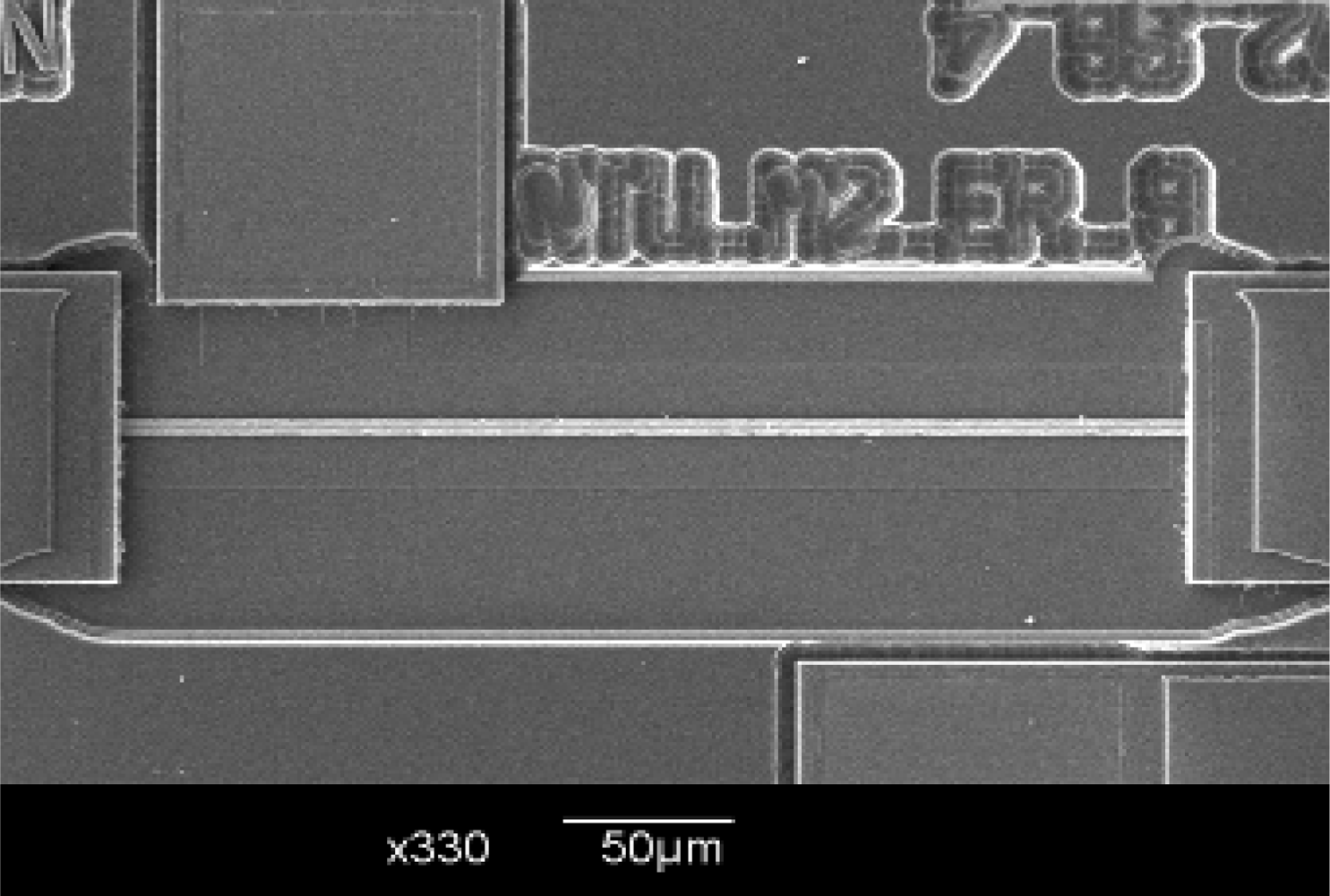
Figure 4 shows SEM pictures of the bridge-type test-key after post-processing, and it is obvious that the test-key is released successfully by soaking in Silox Vapox III for 85 min.
4.2. Pull-in Voltage Detecting
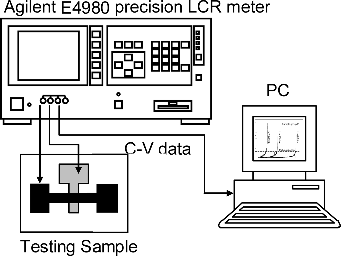
For a deflective microstructure subjected to electrostatic loads, as shown in Figure 1, the structural deflection causes a change in the gap between the upper and bottom electrodes and thus a change in the capacitance. Therefore, the variation of capacitances with the applied bias voltages is equivalent to the deformations to the external loads, and then one can detect the pull-in voltage by tracking the capacitance sensitivities with respect to applied bias voltages. Pull-in will occur when the capacitance shows a sharp increase. Through the capacitance-voltage measurement and the material property extraction algorithms mentioned above, one can obtain the material properties of the test microstructure. The principle of capacitance-voltage measurement is introduced as the following. The main idea is to measure the circuit capacitive reactance XC to yield the capacitance C. The capacitive reactance is Xc = 1/(2π·f·C) where XC, f, and C represent the circuit capacitive reactance, the testing signal frequency, and the capacitance, respectively. The input driving voltage is a small AC testing signal riding on a large DC bias voltage which induces the structural deflection. Then the capacitance can be calculated from the circuit capacitive reactance. It should be mentioned here that the frequency of the AC testing signal must avoid the resonance frequency of the test microstructure; otherwise the capacitance will show a large fluctuation. The Agilent E4980 precision LCR meter is used to measure the capacitance-voltage (C-V) variation of the test microstructure, as shown in Figure 5.
The frequency and level of the AC testing signal must be set properly since they will affect the accuracy of the capacitance measurement. The authors chose the root mean square value of the test AC signal level as 25 mV and the frequency 1 MHz. The integration time is set to medium (MED). The instrument parameters setting are listed in Table 5.
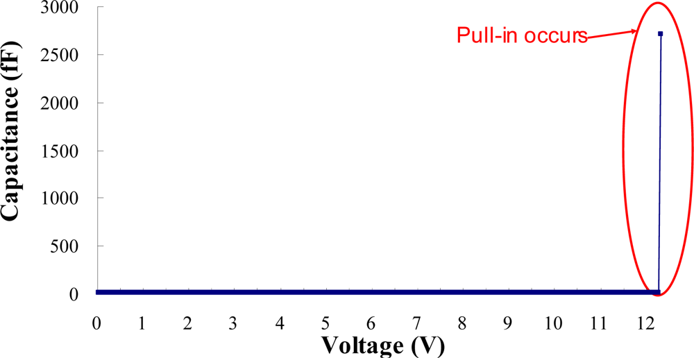
The pull-in voltage is detected by tracking the capacitance sensitivities with respect to the applied bias voltages. Two low noise probes touch the two probing pad of test beam, as shown in Figure 5. The probes are connected to the Agilent E4980 high precision LCR meter, which can supply a test signal of 25 mV/1 MHz riding on the bias voltages ranging from 0 to 40 V. Agilent E4980 exports the capacitance-voltage data to a personal computer and tracks the capacitance sensitivities to the applied bias voltage. Figure 6 shows the typical measured capacitance sensitivities results. Pull-in will occur when the capacitance is with sharp increase. Therefore, according to the results from capacitance-voltage measurement, one can obtain the pull-in voltage of the test beam exactly.
Table 6 lists the geometrical parameters of the bridge-type test beams which are fabricated by a TSMC 0.18 μm 1P6M standard CMOS process. The test beams have the same width, gap, and thickness, but different length. One knows that pull-in occurs when capacitance increases sharply. According to Figure 6, it is obvious that the capacitance will rise up to ten fold or even hundred fold compared to the original capacitance when pull-in occurs. Therefore, one can get the pull-in voltage of test beams, and the corresponding data is shown in Table 7, where VPI-ave is the average value of measured pull-in voltage for five times of each test beam, and ΔVPI is the corresponding standard deviation.
5. Results and Discussion
We substitute the experimental results in Table 7 into Equation (23) to extract Young’s modulus (Ẽ) and mean stress (σ̃0). Table 8 shows the extracted Young’s modulus (Ẽ) and mean stress (σ̃0) of the two test beams when the length difference (ΔL) equals 50 μm. The extracted Young’s modulus (Ẽ) and mean stress (σ̃0) are 132.01 ± 13.48 GPa and 3.4 ± 0.15 MPa, respectively.
This work presents an algorithm for extracting Young’s modulus (Ẽ) and mean stress (σ̃0) of structural materials of CMOS-MEMS devices by detecting the pull-in voltages of two micro bridge-type test beams. The overall deviations of the extracted Young’s modulus (Ẽ) and mean stress (σ̃0) of the demonstrated materials are within 11% and 5%, respectively, when the two test beams have a length difference (ΔL) equal to 50 μm. The present method is very suitable for the implementation of the mechanical characterization of capacitive CMOS-MEMS devices in wafer level testing. The present algorithm can easily be written as a programming code and accompanied by an LCR meter to realize the wafer-level testing for CMOS-MEMS manufacture.
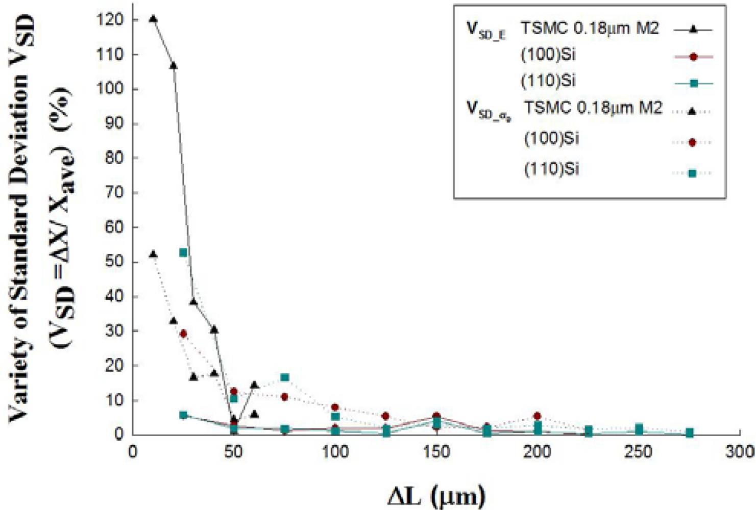
Since this testing method needs to measure pull-in voltages of two test beams with different length, attention should be paid to the appropriate length design of the two test beams. Table 2 lists the geometrical parameters and Figure 7 shows the measured pull-in voltages of the fixed-fixed beams which are made of mono-crystalline silicon in published work [9]. The author selected any two beams and substituted the measured data and beam dimensions into Equation (23) to extract the Young’s modulus (Ẽ) and mean stress (σ̃0). The same procedure is used to deal with the experimental results in Table 7, where the test beams are fabricated by a TSMC 0.18 μm 1P6M standard CMOS process. According to the extracted results, the extracted values show small standard deviations for large ΔL cases but with a large standard deviation for small ΔL cases in two kinds of common structural materials, such as the material made by the TSMC 0.18 μm standard CMOS process, and mono-crystalline silicon in (100) and (110) orientations. The relationship between the difference of test beams (ΔL) and the variation of the extracted values (VSD) by this work is shown in Figure 8. It indicates that the variation of Young’s modulus(VSD_E) and mean stress (VSD_σ0) will reduce by15% when ΔL is larger than 50 μm, even being as low as 2% for ΔL equal to 225 μm in mono-crystalline silicon testing cases. These evidences show that the algorithm presented in this work is robust in extracting mechanical properties at wafer-level testing when test keys with appropriate length design.
6. Conclusions
This paper presents a robust algorithm for extracting Young’s modulus, and mean stress of structural materials of CMOS-MEMS devices. By detecting the pull-in voltages of two bridge-type test beams, and applying the characteristics to the equivalent electromechanical models, and one can know the mechanical properties of thin films. The contributions of this paper may be described in detail as follows:
First, the paper has demonstrated the present method with two common structural materials, such as the material made by the TSMC 0.18 μm standard CMOS process, and mono-crystalline silicon in (100) and (110) orientations. The extracted values by the present method are summarized in Table 9. The overall deviation of the extracted Young’s modulus, mean stress, and gradient stress of the structural materials made by the TSMC 0.18 μm standard CMOS process are within 11% and 5%, respectively. Besides, the deviations of the extracted Young’s modulus and mean stress are within 1% and 2% which are almost tenth of the deviations of Osterberg’s results [9] for mono-crystalline silicon in (100) and (110) orientations. Second, the study of the robustness of the present method with regards to the dimension effects of the test-key is discussed in this paper. For the dimension effects of the test-key, the variations of Young’s modulus (VSD_E) and mean stress (VSD_ σ0) are discussed. According to the results shown in Figure 8, the authors infer that the VSD_E and VSD_ σ0will be reduced within 15% for ΔL larger than 50 μm, and even within 2% for ΔL larger than 225 μm in mono-crystalline silicon testing cases. Therefore, the authors recommend that the two test beams should have a length difference (ΔL) which is larger than 50 μm to decrease the dimension effect. Third, the CMOS-MEMS test-key can be set at the scribe line, and removed after testing. Therefore, it doesn’t need any extra area to proceed with structural material testing. Fourth, the present method is very suitable for the implementation of the mechanical characterization of CMOS-MEMS devices in wafer level testing since the testing signals are electrical signals. Moreover, the present algorithm can easily be written as a programming code and accompanied by an LCR meter to realize wafer-level testing for MEMS manufacture.
Acknowledgments
The authors are thankful for the IC manufacturing support of our research from Taiwan Semiconductor Manufacturing Company (TSMC).
References
- Xie, H.K.; Fedder, G.K. Vertical comb-finger capacitive actuation and sensing for CMOS-MEMS. Sens. Actuators A Phys 2002, 95, 212–221. [Google Scholar]
- Cheng, Y.-C.; Dai, C.-L.; Lee, C.-Y.; Chen, P.-H.; Chang, P.-Z. A MEMS micromirror fabricated using CMOS post-process. Sens. Actuators A Phys 2005, 120, 573–581. [Google Scholar]
- Dai, C.L.; Kuo, C.H.; Chiang, M.C. Microelectromechanical resonator manufactured using CMOS-MEMS technique. Microelectron. J 2007, 38, 672–677. [Google Scholar]
- Petersen, K.E.; Guarnieri, C.R. Young’s modulus measurements of thin films using micromechanics. J. Appl. Phys 1979, 50, 6761–6766. [Google Scholar]
- Zhang, L.M.; Uttamchandani, D.; Culshaw, B. Measurement of the mechanical properties of silicon microresonators. Sens. Actuators A Phys 1991, 29, 79–84. [Google Scholar]
- Kiesewetter, L.; Zhang, J.M.; Houdeau, D.; Steckenborn, A. Determination of Young’s moduli of micromechanical thin films using the resonance method. Sens. Actuators A Phys 1992, 35, 153–159. [Google Scholar]
- Vlassak, J.J.; Nix, W.D. New bulge test technique for the determination of Young’s modulus and Poisson’s ratio of thin films. J. Mater. Res 1992, 7, 3242–3249. [Google Scholar]
- Zou, Q.; Li, Z.; Liu, L. New methods for measuring mechanical properties of thin films in micromachining: beam pull-in voltage (VPI) method and long beam deflection (LBD) method. Sens. Actuators A Phys 1995, 48, 137–143. [Google Scholar]
- Osterberg, P.M.; Senturia, S.D. M-TEST: A test chip for MEMS material property measurement using electrostatically actuated test structures. J. Microelectromech. Syst 1997, 6, 107–118. [Google Scholar]
- Sharpe, W.N., Jr.; Yuan, B.; Edwards, R.L. New technique for measuring the mechanical properties of thin films. J. Microelectromech. Syst 1997, 6, 193–199. [Google Scholar]
- Johansson, S.; Tenerz, S.J.A.; Tiren, J. Fracture testing of silicon microelements in situ in a scanning electron microscope. J. Appl. Phys 1988, 66, 4799–4803. [Google Scholar]
- Serre, C.; Gorostiza, P.; Perez-Rodriguez, A.; Sanz, F.; Morante, J.R. Measurement of micromechanical properties of polysilicon microstructures with an atomic force microscope. Sens. Actuators A Phys 1998, 67, 215–219. [Google Scholar]
- Serre, C.; Perez-Rodriguez, A.; Morante, J.R.; Gorostiza, P.; Esteve, J. Determination of micromechanical properties of thin films by beam bending measurements with an atomic force microscope. Sens. Actuators A Phys 1999, 74, 134–138. [Google Scholar]
- Chudoba, T.; Schwarzer, N.; Richter, F.; Beck, U. Determination of mechanical film properties of a bilayer system due to elastic indentation measurements with a spherical indenter. Thin Solid Films 2000, 377–378, 366–372. [Google Scholar]
- Guckel, H.; Burns, D.; Rutigliano, C.; Lovell, E.; Choi, B. Diagnostic microstructures for the measurement of intrinsic strain in thin films. J. Micromech. Microeng 1992, 2, 86–95. [Google Scholar]
- Fang, W.; Wickert, J.A. Comments on measuring thin-film stresses using bi-layer micromachined beams. J. Micromech. Microeng 1995, 5, 276–281. [Google Scholar]
- Fang, W.; Wickert, J.A. Determining mean and gradient residual stresses in thin films using micromachined cantilevers. J. Micromech. Microeng 1996, 6, 301–309. [Google Scholar]
- Schweitz, J.-A.; Ericson, F. Evaluation of mechanical materials properties by means of surface micromachined structures. Sens. Actuators A Phys 1999, 74, 126–133. [Google Scholar]
- Fang, W.; Wickert, J.A. Post buckling of micromachined beams. J. Micromech. Microeng 1994, 4, 116–122. [Google Scholar]
- Riester, L.; Blau, P.J.; Lara-Curzio, E.; Breder, K. Nanoindentation with a Knoop indenter. Thin Solid Films 2000, 377–378, 635–639. [Google Scholar]
- Dai, C.L. In situ electrostatic microactuators for measuring the Young’s modulus of CMOS thin films. J. Micromech. Microeng 2003, 13, 563–567. [Google Scholar]
- Marshall, J.C.; Herman, D.L.; Vernier, P.T.; de Voe, D.L.; Gaitan, M. Young’s modulus measurements in standard IC CMOS processes using MEMS test structures. IEEE Electron. Dev. Lett 2007, 28, 960–963. [Google Scholar]
- Li, X.; Ono, T.; Wang, Y.; Esashi, M. Ultrathin single-crystalline-silicon cantilever resonators: Fabrication technology and significant specimen size effect on Young’s modulus. Appl. Phys. Lett 2003, 83, 3081–3083. [Google Scholar]
- Yang, J.; Ono, T.; Esashi, M. Mechanical behavior of ultrathin microcantilever. Sens. Actuators A Phys 2000, 82, 102–107. [Google Scholar]
- Smee, S.A.; Gaitan, M.; Novotny, D.B.; Joshi, Y.; Blackburn, D.L. IC test structures for multilayer interconnect stress determination. IEEE Electron. Dev. Lett 2000, 21, 12–14. [Google Scholar]
- Najafi, K.; Suzuki, K. Novel Technique and Structure for the Measurement of Intrinsic Stress and Young’s Modulus of Thin Films. Proceedings of the Micro Electro Mechanical Systems: An Investigation of Micro Structures, Sensors, Actuators, Machines and Robots, Salt Lake, UT, USA, 20–22 February 1989; pp. 96–97.
- Gupta, R.K.; Osterberg, P.M.; Senturia, S.D. Material property measurements of micromechanical polysilicon beams. Proc. SPIE Int. Soc. Opt. Eng 1996, 2880, 39–45. [Google Scholar]
- Oliver, W.C.; Pharr, G.M. An improved technique for determining hardness and elastic modulus using load and displacement sensing indentation experiments. J. Mat. Res 1992, 7, 1564–1583. [Google Scholar]
- Klein, C.A. How accurate are Stoney’s equation and recent modifications. J. Appl. Phys 2000, 88, 5487–5489. [Google Scholar]
- Guckel, H.; Burns, D.W.; Tilmans, H.A.C.; DeRoo, D.W.; Rutigliano, C.R. Mechanical Properties of Fine Grained Polysilicon—The Repeatability Issue. Proceedings of the Components, Circuits, Devices & Systems; Engineered Materials, Dielectrics & Plasmas; Robotics & Control Systems; Signal Processing & Analysis, Hilton Head, SC, USA, 6–9 June 1988; pp. 96–99.
- Guckel, H.; Burns, D.W.; Tilmans, H.A.C.; Visser, C.C.G.; DeRoo, D.W.; Christenson, T.R.; Klomberg, P.J.; Sniegowski, J.J.; Jones, D.H. Processing Conditions for Polysilicon Films with Tensile Strain for Large Aspect Ratio Microstructures. Proceedings of the Components, Circuits, Devices & Systems; Engineered Materials, Dielectrics & Plasmas; Robotics & Control Systems; Signal Processing & Analysis, Hilton Head, SC, USA, 6–9 June 1988; pp. 51–56.
- Guckel, H.; Burns, D.W.; Visser, C.C.G.; Tilmans, H.A.C.; Deroo, D. Fine-grained polysilicon films with built-in tensile strain. IEEE Trans. Electron. Dev 1988, 35, 800–801. [Google Scholar]
- Wylde, J.; Hubbard, T.J. Elastic Properties and Vibration of Micro-Machined Structures Subject to Residual Stresses. Proceedings of the Canadian Conference on Electrical and Computer Engineering, Edmonton, Canada, 9–12 May 1999; pp. 1674–1679.
- Sun, X.-Q.; Li, Z.; Zheng, X.; Liu, L. Study of fabrication process of a micro electrostatic switch and its application to a micromechanical V-F converter. Sens. Actuators A Phys 1993, 35, 189–192. [Google Scholar]
- Gupta, R.K. Electrostaic Pull-in Test Structure Design for in situ Mechanical Property Measurements of Microelectromechanical Systems; Ph.D. Dissertation,; Massachusetts Institute of Technology: Cambridge, MA, USA, 1997. [Google Scholar]
- Lin, R.M.; Wang, W.J. Structural dynamics of microsystems—Current state of research and future direction. Mech. Syst. Signal Process 2006, 20, 1015–1043. [Google Scholar]
- Chuang, W.C.; Wang, C.W.; Chu, W.C.; Chang, P.Z.; Hu, Y.C. The fringe capacitance formula of microstructures. J. Micromech. Microeng. 2012, 22. [Google Scholar] [CrossRef]
- Soedel, W. Vibrations of Shells and Plates; Marcel Dekker: New York, NY, USA, 1993. [Google Scholar]
- Spiegel, M.R. Mathematical Handbook of Formulas and Tables; McGraw-Hill: New York, NY, USA, 1987. [Google Scholar]


| Measuring methods | Actuating methods | |||||
|---|---|---|---|---|---|---|
| Electrostatic | Vibration | Pulsed laser light | Force/Pressure | Thermal | Pre-deformation | |
| Interferometer | [4,5,8,21,30–32] | [6,22] | [23,24] | [7,10,33] | [15,30–32] | [16,17,19,25] |
| Nanoindenter | [14,20] | |||||
| AFM | [12,13] | |||||
| SEM | [11] | |||||
| μ strain gauge | [18] | |||||
| XRD | [14,20] | |||||
| V-F converter | [34] | |||||
| Pull-in | [9,26,27,35] | |||||
| Parameters | Values | |||||
|---|---|---|---|---|---|---|
| Permeability of free space ε (F/m) | 8.85 × 10⁻¹² | |||||
| Initial gap g (μm) | 1.05 | |||||
| Beam width b (μm) | 50 | |||||
| Beam thickness h (μm) | 2.94 | |||||
| Length L of group 1 | 175 | 400 | 225 | 450 | 275 | 500 |
| Measured pull-in voltage VPI (V) | 77.38 | 16.9 | 47.79 | 13.78 | 32.65 | 11.56 |
| Length L of group 2 | 175 | 450 | 225 | 500 | 275 | 550 |
| Measured pull-in voltage VPI (V) | 85.22 | 14.78 | 52.68 | 12.4 | 36 | 10.61 |
| Length (μm) | The values extracted by this work | M-test [9] | |||
|---|---|---|---|---|---|
| L1 | L2 | E (GPa) | σ0 (MPa) | E (GPa) | σ0 (MPa) |
| 175 | 400 | 135.35 | 9.97 | ||
| 225 | 450 | 135.21 | 9.68 | 138 ± 4 | 10 ± 2 |
| 275 | 500 | 134.40 | 9.66 | ||
| Average (Xave) | 134.99 | 9.77 | 138 | 10 | |
| Standard Deviation (ΔX) | 0.42 | 0.14 | 4 | 2 | |
| Variety of Standard Deviation VSD (VSD = ΔX/Xave) | 0.31% | 1.45% | 2.90% | 20.00% | |
| Length (μm) | The values extracted by this work | M-test [9] | |||
|---|---|---|---|---|---|
| L1 | L2 | E (GPa) | σ0 (MPa) | E (GPa) | σ0 (MPa) |
| 175 | 450 | 166.88 | 9.50 | 168 ± 6 | 10 ± 1 |
| 225 | 500 | 168.16 | 9.53 | ||
| 275 | 550 | 167.40 | 9.69 | ||
| Average (Xave) | 167.48 | 9.57 | 168 | 10 | |
| Standard Deviation (ΔX) | 0.53 | 0.08 | 6 | 1 | |
| Variety of Standard Deviation VSD (VSD =ΔX/Xave) | 0.31% | 0.87% | 3.57% | 10.00% | |
| Function | Cp-D |
|---|---|
| Testing Signal Frequency | 1 MHz |
| Testing Signal Level | 0.025 V |
| Bias Voltage Range | 0–40 V |
| Bias Voltage Step | 0.05 V |
| Integration Time | Med |
| Parameters | Values |
|---|---|
| Beam width b (μm) | 5 |
| Initial gap g (μm) | 1.93 |
| Beam thickness h (μm) | 0.53 |
| Beam length L (μm) | 220−300 |
| Length L (μm) | Vpull-in VPI (V) | Average VPI-ave (V) | Standard Deviation ΔVPI |
|---|---|---|---|
| 220 | 12.27,12.32,12.32,12.47,12.82 | 12.44 | 0.20 |
| 230 | 11.56,11.71,11.76,12.27,12.37 | 11.93 | 0.32 |
| 240 | 10.91,11.41,11.46,11.51,11.56 | 11.36 | 0.23 |
| 250 | 9.76,10.46,10.71,10.91,11.11 | 10.59 | 0.47 |
| 260 | 9.76,10.06,10.16,10.26,10.56 | 10.16 | 0.26 |
| 270 | 9.01, 9.11,9.52, 9.71, 9.96 | 9.46 | 0.36 |
| 280 | 8.81, 8.86,8.86 ,9.16, 9.51 | 9.04 | 0.27 |
| 290 | 8.06, 8.61, 8.86, 8.86,9.51 | 8.78 | 0.47 |
| 300 | 8.06 ,8.11, 8.31, 8.56,8.61 | 8.33 | 0.22 |
| Length difference (μm) | Length (μm) | The extracted values by this work | ||
|---|---|---|---|---|
| ΔL | L1 | L2 | E (GPa) | σ0 (MPa) |
| 50 | 220 | 270 | 112.75 | 3.56 |
| 230 | 280 | 147.87 | 3.15 | |
| 240 | 290 | 140.74 | 3.41 | |
| 250 | 300 | 126.68 | 3.48 | |
| Average (Xave) | 132.01 | 3.40 | ||
| Standard Deviation (ΔX) | 13.48 | 0.15 | ||
| Variety of Standard Deviation VSD (VSD =ΔX/Xave) | 10.21% | 4.52% | ||
| Common Structural Material | The extracted values by this work | |
|---|---|---|
| metal 2 made by the TSMC 0.18 μm standard CMOS process | E(GPa) | σ0(MPa) |
| 132.01 ± 13.48 | 3.4 ± 0.15 | |
| mono-crystalline silicon in (100) | 134.9 9± 0.42 | 9.77 ± 0.14 |
| mono-crystalline silicon in (110) | 167.48 ± 0.53 | 9.57 ± 0.08 |
© 2012 by the authors; licensee MDPI, Basel, Switzerland This article is an open access article distributed under the terms and conditions of the Creative Commons Attribution license (http://creativecommons.org/licenses/by/3.0/).
Share and Cite
Chuang, W.-C.; Hu, Y.-C.; Chang, P.-Z. CMOS-MEMS Test-Key for Extracting Wafer-Level Mechanical Properties. Sensors 2012, 12, 17094-17111. https://doi.org/10.3390/s121217094
Chuang W-C, Hu Y-C, Chang P-Z. CMOS-MEMS Test-Key for Extracting Wafer-Level Mechanical Properties. Sensors. 2012; 12(12):17094-17111. https://doi.org/10.3390/s121217094
Chicago/Turabian StyleChuang, Wan-Chun, Yuh-Chung Hu, and Pei-Zen Chang. 2012. "CMOS-MEMS Test-Key for Extracting Wafer-Level Mechanical Properties" Sensors 12, no. 12: 17094-17111. https://doi.org/10.3390/s121217094