A CMOS-Compatible Poly-Si Nanowire Device with Hybrid Sensor/Memory Characteristics for System-on-Chip Applications

Abstract
: This paper reports a versatile nano-sensor technology using “top-down” poly-silicon nanowire field-effect transistors (FETs) in the conventional Complementary Metal-Oxide Semiconductor (CMOS)-compatible semiconductor process. The nanowire manufacturing technique reduced nanowire width scaling to 50 nm without use of extra lithography equipment, and exhibited superior device uniformity. These n type polysilicon nanowire FETs have positive pH sensitivity (100 mV/pH) and sensitive deoxyribonucleic acid (DNA) detection ability (100 pM) at normal system operation voltages. Specially designed oxide-nitride-oxide buried oxide nanowire realizes an electrically Vth-adjustable sensor to compensate device variation. These nanowire FETs also enable non-volatile memory application for a large and steady Vth adjustment window (>2 V Programming/Erasing window). The CMOS-compatible manufacturing technique of polysilicon nanowire FETs offers a possible solution for commercial System-on-Chip biosensor application, which enables portable physiology monitoring and in situ recording.1. Introduction
Nanotechnology is being widely investigated in biosensor development to supplant traditional chemical biomolecules detection [1,2]. Different sensitive methods, including optical-based detection (surface plasmon resonance), mechanically based detection (cantilevers), and electrical-based detection (capacitive electrode and nanowire device) are attractive in a number of biomolecule application fields [1–7]. Among them, semiconducting nanowire FET sensors [4] have a great potential to function as label-free, highly accurate, and real-time detectors of low concentrations of proteins [5,8], viruses [6], and DNA [7,9]. Compared to other detection methods, the detection functionality of a nanowire sensor is verified through pure electrical signal characterization; therefore, neither special devices nor materials are necessary. Thus, the production costs could potentially be reduced compared to other sensors. In certain studies, semiconductor nanowires were prepared by the “bottom-up” process [4], which leads to several commercialization problems because of the difficulties of positioning individual nanowires. Consequently, various “top-down” processes for fabricating silicon nanowires have been proposed to provide a solution for manufacturing reliable biosensors because of its compatibility with current commercial silicon-based CMOS technology [6,10]. However, to obtain a large surface-to-volume ratio nanowire with extraordinary detection sensitivity, special techniques or advanced lithography tools were employed to achieve the slender nanowire patterns [10,11]. Therefore, determining an approach on the quick fabrication of a large amount of reliable devices, controlling the electrical properties response at relatively simple detection, and reducing productive costs in commercial scale will be an important issue for using silicon nanowire FETs in future biomedical applications [12].
Table 1 shows a comparison of the Si nanowire FET fabrication in previous studies [4–6,10–14] and this work. Most semiconductor nanowires composed using the “bottom-up” process [4–6] display good detection performances, but are difficult to mass produce and integrate with the CMOS process. Moreover, the “top-down” process [10,13–15] requires advanced exposed equipment (e-beam lithography) or a special pattern design to improve nanowire uniformity and sensitivity. Although numerous studies have been performed for improving nanowire detection sensitivity [14], CMOS circuit integration with signal processing and data storing remains deficient. In this study, a System-on-Chip biosensor was developed using “top-down” poly-Si nanowire FETs in the conventional CMOS-compatible process. To embed nanowire FETs at the back end of line (BEOL) stage of a VLSI circuit, the fabrication of thin-film transistors with poly-Si nanowire channels were employed for low-cost semiconductor manufacturing [16]. With no expensive lithography tools and with desirable process compatibility, the poly-Si nanowire sensor fabrication is favorable for traditional CMOS integration. Furthermore, the electrical characteristics of the nanowire devices can be adjusted by programming or erasing the nitride charge of the specially designed oxide-nitride-oxide (ONO)-buried oxide [17]. This embedded EEPROM cell can be integrated easily into the sensor circuit. The combination of sensor, memory, and circuit in the CMOS-compatible process provides a system-scale integration solution of smart biosensor application for low-cost commercial manufacturing [18].
2. Samples Preparation
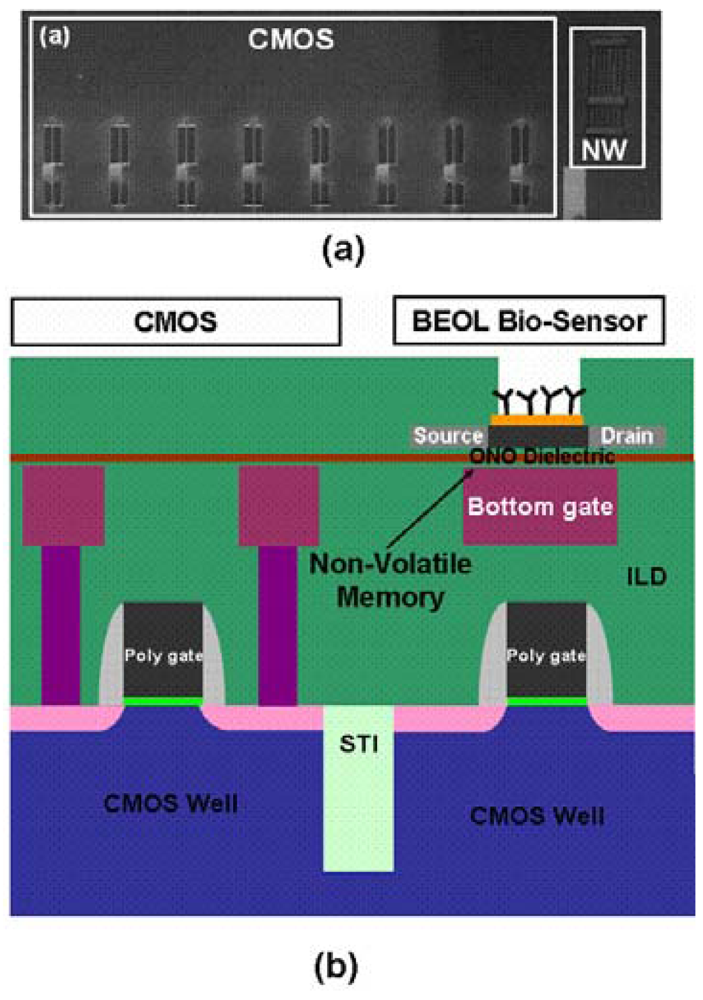
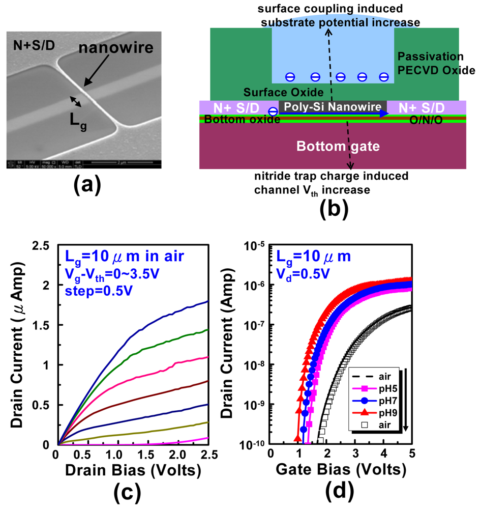
The device samples were manufactured on standard 6-in. p-type wafers. A proposed hybrid sensor/memory/CMOS poly-Si nanowire structure is illustrated in Figure 1(b). The bottom-gate poly-Si nanowire formation can be inserted specifically after metallization of the back-end process (BEOL). At the beginning, buried oxide was deposited on a substrate surface as the gate dielectric of nanowire FETs. A 50-nm polysilicon layer was then deposited using the CVD process. Subsequently, the poly-Si wire was patterned by the standard I-line stepper of the CMOS semiconducting process. By using reactive plasma etching for photoresist trimming followed by silicon etching, the nanowire dimension was scaled to a level of approximately 100 nm. A nanowire shrinkage technique using poly re-oxidation and oxide stripping was employed to scale down the nanowire width to less than 50 nm. A channel protection photoresist pattern was then formed by I-line lithography. The objective of the channel protection patterning was to keep the channel intrinsically from n+ source/drain (S/D) implantation, to increase nanowire FETs sensitivity. Subsequently, the n+ S/D implant was performed with a 1015 cm−2 P31+ ion beam at 10 keV to reduce the parasitic resistance of the nanowire. Thereafter, the channel protection photoresist was removed. Finally, the S/D dopant was activated by annealing treatment at 600 °C for 30 min in a N2 ambience. The top-view SEM image of the hybrid sensor/memory/CMOS circuit is shown in Figure 1(a). The fabrication flow requires only two extra masks and can be integrated into a standard BEOL process. Figure 2(a) shows the SEM image of the nanowire devices, and Figure 2(b) illustrates the operation mode diagram of the bottom-gate poly-Si nanowire device for ionic solution detection and nitride trap charge storing. Figure 2(c,d) plot the Id-Vg and Id-Vd characteristics of the poly-Si nanowire FETs. The device on-off ratio is approximately 105, and the subthreshold swing is 0.5 V/dec. The device threshold voltage was defined by the gate bias at a constant current:
3. Experimental Characteristics
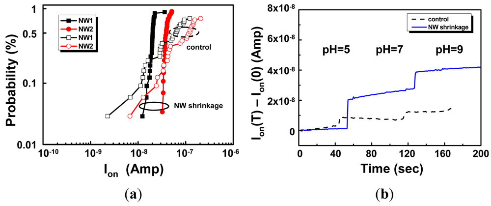
The mass manufacture of the semiconductors can simultaneously hold 32 dies in each 6-in. wafer. Figure 3(a) shows the statistics of a comparison among the electrical characteristics of various wire widths without and with the nanowire shrinkage process. The driving current Ion is measured, with a bottom gate of 5 V and a drain bias of 0.5 V, without any fluid on the nanowire surface. After the shrinkage process, the statistical plot shows less variation tailing for the improvement of PR trimming-induced surface roughness. Because device-to-device variation can be controlled significantly using the shrinkage process, pH sensitivity testing or memory characteristics in this paper are completed for individual nanowire devices, for fair comparison. On the side, the surface adhesion stress of fluidic cell spatial deflection [19] can also be aligned for nanowire structure uniformity. Figure 3(b) displays Ion versus time data as phosphate buffer solutions, with pH levels of 5, 7, and 9, which were sequentially delivered onto the nanowire sensors without surface treatment. The nanowire shrinkage split has a high Ion change caused by the large surface-to-volume ratio. The functionality of the poly-Si nanowire sensor can improve Ion accumulation distribution, and further enhance electrical pH sensitivity. Thus, the pH sensors of the poly-Si nanowire FETs not only have a higher manufacturing production yield, but also have a greater tolerance for the signal-to-noise ratio [20], for future single-chip system integration of nano-sensors.
4. Results and Discussion
4.1. Nanowire for Biosensor Application
Figure 2(d) also shows the Id-Vg curves of the n-type poly-Si nanowire FETs in different pH solutions flowing without surface treatment. The testing sequence is indicated by the arrow. No I-V degradation is present after pH testing, and it displays an obvious Vth decrease and Ion increase with a rising pH value. The superior pH sensitivity (>100 mV/pH) is an opposite property and beyond the Nernst limitation (60 mV/pH) to ion-selective FETs [21,22]. The Ion increases and returns to its original value as the pH value rises from 5, 7, and 9, and reverses sequentially (Figure 4(a)). Consequently, the positive current shifts (10%/pH) are repeatable in the n-type poly-Si nanowire sensors. Figure 4(b) shows the schematic band diagram of the nanowire sensor to explain the Ion increase. The bottom-gate FETs' electrical behavior could be controlled by the substrate ionic concentration coupling induced the channel substrate potential modification [23]. The surface oxide coupling effect enables the nanowire substrate potential to have an opposite polarity from the ionic strength of the pH solution. The threshold voltage Vth of the poly-Si nanowire FETs determines the current flow in the nanowire channel, which can be described as in [24]:
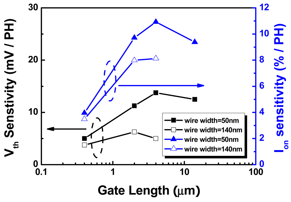
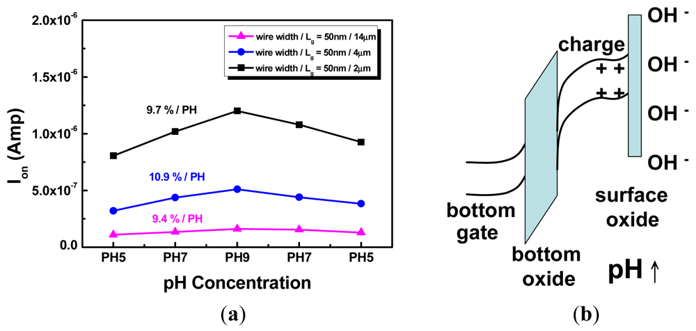
This work also evaluates the pH sensitivity of the poly-Si nanowire FET sensor responses at various nanowire geometries. Figure 5 shows the driving current sensitivity and Vth shift with different pH solutions in various nanowire widths and channel length conditions. In the nanowire width direction, narrower width devices have higher pH sensitivity, which is consistent with most previous studies [25]. However, a short channel split did not show apparent pH sensitivity in the experiment of this paper. The short channel devices had a smaller intrinsic channel area, and the rest of the nanowire was doped with a heavy S/D dopant to reduce parasitic resistance of the nanowire and the influence of noise. The channel-coupling effect is attenuated at the heavy-doped nanowire region, thereby reducing the pH sensitivity of the short channel nanowire. Although short channel devices have large current shifts in different pH solutions (Figure 4(a)), the higher conduction current from the short channel device loses the nanowire potential control ability and pH sensitivity. Thus, the proper geometrical design to optimize device sensitivity and noise tolerance is a crucial consideration in the improvement of detection sensitivity in nanowire FET sensors.
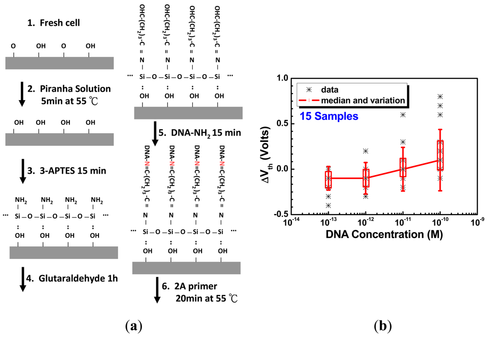
The primer DNA detection of the poly-Si nanowire FET sensors is also tested in this work. Figure 6(a) shows a schematic illustration of the poly-Si nanowire surface treatment steps for DNA concentration detection. First, the fresh nanowire surface was washed with piranha solution for 5 min to form a uniform OH bond. Subsequently, the 3-APTES solution was coated to link glutaraldehyde. After the series treatment process, the oligo DNA could be bound effectively on the nanowire surface to react with subsequent primer DNA. The Vth shift of the poly-Si nanowire FETs at various primer DNA concentrations is shown in Figure 6(b). Every condition indicates the median of the 15 devices at the same wafer, and the standard deviation is also shown. Approximately 100 mV of the Vth shift is still present as the primer DNA concentration is lowered to 10 pM. The concentration sensitivity is substantially higher than the conventional PCR limitation. This result demonstrates that the poly-Si nanowire FET sensors have high potential for DNA detection and application in gene engineering.
4.2. Nanowire as Stacked Memory
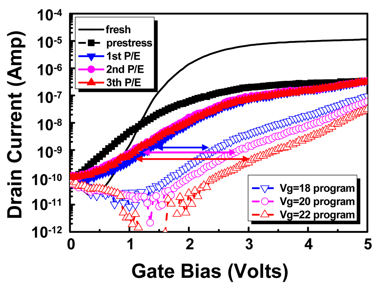
Specially designed ONO-buried oxide of the poly-Si nanowire was realized to obtain the charge storage layer of the memory application. In a high dielectric field, the nitride trap charge of the ONO-buried oxide can be filled or removed, and subsequently, the nanowire substrate channel potential would be modified. Figure 7 plots the Id-Vg characteristics of the ONO-buried oxide poly-Si nanowire FETs at different operation modes in a single nanowire device. After a short initial high negative gate bias pre-stress, the Id-Vg curve of the poly-Si nanowire FETs can be shifted to a relatively low Vth level because the trap charge of the buried oxide was neutralized. The Id-Vg curve can be erased effectively to the steady Vth level through a short erase pulse (10 ms), and Vth can be adjusted after achieving an adequate programming condition. Furthermore, the electrical characteristics of various operation conditions are reappearance.
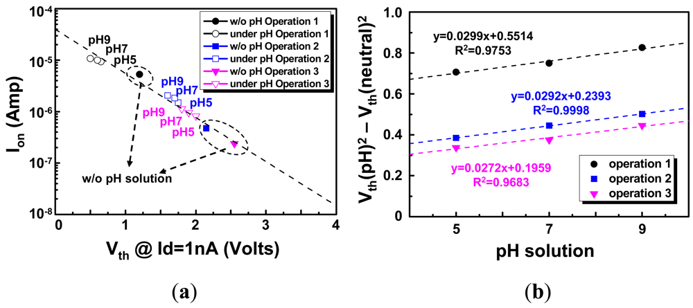
The pH testing of the ONO-buried oxide poly-Si nanowire FETs was also implemented at various Vth levels. First, we recorded the initial Vth level and operated the pH testing at the initial state, designated operation 1 (at erase state, Vg = −12 V). Subsequently, the ONO-buried oxide nanowire device was programmed to a high Vth level, and operated the pH testing at a high Vth state, designated operation 2 (at program state, Vg = 18 V). Finally, a higher programming bias, designated operation 3 (at program state, Vg = 20 V), was operated in the same device to obtain a higher Vth level, and preceded pH testing. Figure 8(a) shows that the Vth shifts of surface pH ionic coupling and nitride charge trapping follow the same Ion-Vth trend. Its pH sensitivity at a normalized scale Vth(pH)2-Vth(neutral)2 is plotted in Figure 8(b). Similar pH sensitivity slopes are in different Vth levels, and they are consisten with a previous pH ionic substrate-coupling model, as shown in Equation (3). The strongly Vth-adjustable nanowire device provides a consistent electrical response for self-alterable correction and memory-integrated application.
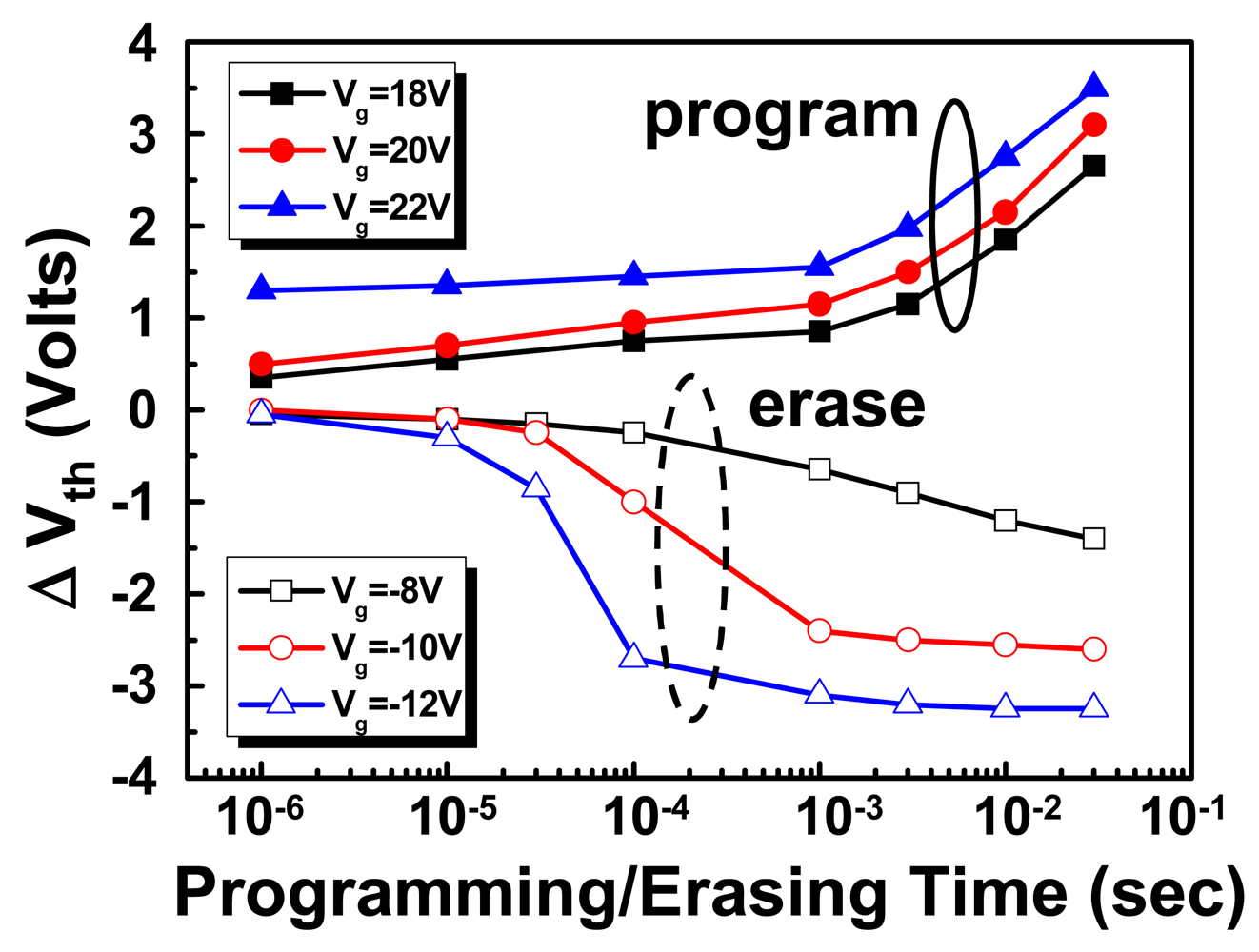
Figure 9 shows a comparison of the programming and erasing efficiency characteristics of the ONO-buried oxide poly-Si nanowire FETs. The Vth shifts are over 3 V when programming/erasing time is approximately 10 ms at the adequate operation bias. Its endurance characteristics are shown in Figure 10(a). The programming and erasing Vg bias conditions are 20 V and −12 V, respectively. The programming/erasing cycles is shown to be more than 105 operation cycles with an acceptable memory Vth programming/erasing window. The data retention characteristics are also shown in Figure 10(b). The memory programming/erasing window is still larger than 2 V after a long storage period of 3 days. These reliability characteristics both demonstrate that the ONO-buried oxide poly-Si nanowire FETs have great potential as the EEPROM cell in embedded memory applications. This approach to Vth-adjustable nanowire FETs provides a possible System-on-Chip solution for self-alterable correcting and in situ recording.
Figure 9 shows a comparison of the programming and erasing efficiency characteristics of the ONO-buried oxide poly-Si nanowire FETs. The Vth shifts are over 3 V when the programming/erasing time is approximately 10 ms at the adequate operation bias. Its endurance characteristics are shown in Figure 10(a). The programming and erasing Vg bias conditions are 20 V and −12 V, respectively. The programming/erasing cycles is shown to be more than 105 operation cycles with an acceptable memory Vth programming/erasing window. The data retention characteristics are also shown in Figure 10(b). The memory programming/erasing window is still larger than 2 V after a long storage period of 3 days. These reliability characteristics both demonstrate that the ONO-buried oxide poly-Si nanowire FETs have great potential as the EEPROM cell in embedded memory applications. This approach to Vth-adjustable nanowire FETs provides a possible System-on-Chip solution for self-alterable correcting and in situ recording.
5. Conclusions
In conclusion, this paper reports a Vth-adjustable nanowire biosensor integrated with a sensor/memory/CMOS application in a fully semiconducting process that provides a possible solution for the realization of System-on-Chip IC fabrication. The nanowire FETs have a distinct pH-sensitive slope (Vth shift > 100 mV/pH) and sensible DNA concentration detection (Vth shift > 100 mV in 10 pM). The strongly Vth-adjustable nanowire FETs of the oxide-nitride-oxide buried oxide provide a consistent electrical response for self-alterable correction. Furthermore, the specially designed oxide-nitride-oxide buried oxide nanowire also demonstrates robust endurance and retention characteristics (>2 V programming/erasing window after 100 K programming/erasing cycles or 3-day storage) as embedded non-volatile memory application.
Acknowledgments
This work was performed by the National Nano Device Laboratories facilities and was supported by the National Science Council, Taiwan.
References
- Khaled, A.R.A.; Vafai, K.; Yang, M.; Zhang, X.; Ozkan, C.S. Analysis, control and augmentation of microcantilever deflections in bio-sensing systems. Sens. Actuat. B 2003, 94, 103–115. [Google Scholar]
- Patolsky, F.; Lieber, C.M. Nanowire nanosensors. Materialtoday 2005, 8, 20–28. [Google Scholar]
- Curreli, M.; Zhang, R.; Ishikawa, F.N.; Chang, H.K.; Cote, R.J.; Zhou, C.; Thompson, M.E. Real-time, label-free detection of biological entities using nanowire-based FETs. IEEE Trans. Nanotechnol. 2008, 7, 651–667. [Google Scholar]
- Cui, Y.; Wei, Q.; Park, H.; Lieber, C.M. Nanowire nanosensors for highly sensitive and selective detection of biological and chemical species. Science 2001, 293, 1289–1292. [Google Scholar]
- Kim, A.; Ah, C.S.; Yu, H.Y.; Yang, J.H.; Baek, I.B.; Ahn, C.G.; Park, C.W.; Jun, M.S.; Lee, S. Ultrasensitive, label-free, and real-time immunodetection using silicon field-effect transistors. Appl. Phys. Lett. 2007, 91, 103901–103903. [Google Scholar]
- Stern, E.; Klemic, J.F.; Routenberg, D.A.; Wyrembak, P.N.; Turner-Evans, D.B.; Hamilton, A.D.; LaVan, D.A.; Fahmy, T.M.; Reed, M.A. Label-free immunodetection with CMOS-compatible semiconducting nanowires. Nature 2007, 445, 519–522. [Google Scholar]
- Zhang, G.J.; Zhang, G.; Chua, J.H.; Chee, R.E.; Wong, E.H.; Agarwal, A.; Buddharaju, K.D.; Singh, N.; Gao, Z.; Balasubramanian, N. DNA sensing by silicon nanowire: charge layer distance dependence. Nano Lett. 2008, 8, 1066–1070. [Google Scholar]
- Chua, J.H.; Chee, R.E.; Agarwal, A.; Wong, S.M.; Zhang, G.J. Label-free electrical detection of cardiac biomarker with complementary metal-oxide semiconductor-compatible silicon nanowire sensor arrays. Anal. Chem. 2009, 81, 6266–6271. [Google Scholar]
- Hahm, J.I.; Lieber, C.M. Direct ultrasensitive electrical detection of DNA and DNA sequence variations using nanowire nanosensors. Nano Lett. 2004, 4, 51–54. [Google Scholar]
- Lin, H.C.; Lee, M.H.; Su, C.J.; Huang, T.Y.; Lee, C.C.; Yang, Y.S. A simple and low-cost method to fabricate TFTs with poly-si nanowire channel. IEEE Electron. Device Lett. 2005, 26, 643–645. [Google Scholar]
- Hsiao, C.Y.; Lin, C.H.; Hung, C.H.; Su, C.J.; Lo, Y.R.; Lee, C.C.; Lin, H.C.; Ko, F.H.; Huang, T.Y.; Yang, Y.S. Novel poly-silicon nanowire field effect transistor for biosensing application. Biosens. Bioelectron. 2009, 24, 1223–1229. [Google Scholar]
- Ahn, J.H.; Kim, J.Y.; Jung, C.; Moon, D.I.; Choi, S.J.; Kim, C.H.; Lee, K.B.; Park, H.G.; Choi, Y.K. CMOS-based biosensors with an independent double-gate finFET. Proceedings of 2011 IEEE International Electron Device Meeting (IEDM), Washington DC, USA, 5–7 December 2011; pp. 852–855.
- Elibol, O.H.; Reddy, B., Jr.; Bashir, R. Nanoscale thickness double-gated field effect silicon sensors for sensitive pH detection in fluid. Appl. Phys. Lett. 2008, 92, 193904–193906. [Google Scholar]
- Shin, K.S.; Lee, K.; Kang, J.Y.; Chui, C.O. Novel t-channel nanowire FET built-in signal amplification for pH sensing. Proceedings of 2009 IEEE International Electron Device Meeting (IEDM), Baltimore MD, USA, 7–9 December 2009; pp. 599–602.
- Park, I.; Li, Z.; Pisano, A.P.; Williams, R.S. Top-down fabricated silicon nanowire sensors for real-time chemical detection. Nanotechnology 2010, 21, 1–9. [Google Scholar]
- Lin, H.C.; Su, C.J. High-performance poly-Si nanowire NMOS transistors. IEEE Trans. Nanotechnol. 2007, 6, 206–212. [Google Scholar]
- Chen, M.C.; Chen, H.Y.; Lin, C.Y.; Tsai, C.M.; Hsieh, C.F.; Horng, J.T.; Qiu, J.T.; Huang, C.C.; Yang, F.L. A novel smart nanowire biosensor with hybrid sensor/memory/CMOS technology. Proceedings of 2010 IEEE International Electron Device Meeting (IEDM), San Francisco, CA, USA, 6–8 December 2010; pp. 820–823.
- Widdershoven, F.; van Steenwinckel, D.; Überfeld, J.; Merelle, T.; Suy, H.; Jedema, F.; Hoofman, R.; Tak, C.; Sedzin, A.; Cobelens, B.; et al. CMOS biosensor platform. Proceedings of 2010 IEEE International Electron Device Meeting (IEDM), San Francisco, CA, USA, 6–8 December 2010; pp. 816–819.
- Khaled, A.R.A.; Vafai, K. Optimization modeling of analyte adhesion over an inclined microcantilever-based biosensor. J. Micromech. Microeng. 2004, 14, 1220–1229. [Google Scholar]
- Lee, J.W.; Jang, D.; Kim, G.T.; Mouis, M.; Ghibaudo, G. Analysis of charge sensitivity and low frequency noise limitation in silicon nanowire sensors. J. Appl. Phys. 2010, 107, 44501–44504. [Google Scholar]
- Chen, Y.; Wang, X.; Erramilli, S.; Mohanty, P. Silicon-based nanoelectronic field-effect pH sensor with local gate control. Appl. Phys. Lett. 2006, 89, 223512–223514. [Google Scholar]
- Gao, X.P.A.; Zheng, G.; Lieber, C.M. Subthreshold regime has the optimal sensitivity for nanowire FET biosensors. Nano Lett. 2010, 10, 547–552. [Google Scholar]
- Knopfmacher, O.; Tarasov, A.; Fu, W.; Wipf, M.; Niesen, B.; Calame, M.; Schonenberger, C. Nernst limit in dual-gated si-nanowire FET sensors. Nano Lett. 2010, 10, 2268–2274. [Google Scholar]
- Bergveld, P. Thirty years of ISFETOLOGY what happened in the past 30 years and what may happen in the next 30 years. Sens. Actuat. B 2003, 88, 1–20. [Google Scholar]
- Nair, P.R.; Alam, M.A. Design considerations of silicon nanowire biosensors. IEEE Trans. Electron Devices 2007, 54, 3400–3408. [Google Scholar]


| Ref. | NW formation | NW material | NW uniformity | Process complexity | Fabrication cost | CMOS compatibility | pH sensitivity |
|---|---|---|---|---|---|---|---|
| bottom-up [4] | CVD | Si | high | × | × | × | 10%/pH |
| bottom-up [5] | RIE(Dry) | SOI | high | simple | × | × | - |
| bottom-up [6] | TMAH(Wet) | SOI | high | × | × | good | 20×/pH |
| bottom-up [13] | E-beam | SOI | × | × | × | good | 7×/pH |
| bottom-up [14] | E-beam | SOI | × | simple | × | good | 15%/pH |
| bottom-up [10] | Spacer | poly-Si | × | simple | cheap | good | - |
| This work | BEOL | poly-Si | simple | cheap | good | 10%/pH |
© 2012 by the authors; licensee MDPI, Basel, Switzerland. This article is an open access article distributed under the terms and conditions of the Creative Commons Attribution license (http://creativecommons.org/licenses/by/3.0/).
Share and Cite
Chen, M.-C.; Chen, H.-Y.; Lin, C.-Y.; Chien, C.-H.; Hsieh, T.-F.; Horng, J.-T.; Qiu, J.-T.; Huang, C.-C.; Ho, C.-H.; Yang, F.-L. A CMOS-Compatible Poly-Si Nanowire Device with Hybrid Sensor/Memory Characteristics for System-on-Chip Applications. Sensors 2012, 12, 3952-3963. https://doi.org/10.3390/s120403952
Chen M-C, Chen H-Y, Lin C-Y, Chien C-H, Hsieh T-F, Horng J-T, Qiu J-T, Huang C-C, Ho C-H, Yang F-L. A CMOS-Compatible Poly-Si Nanowire Device with Hybrid Sensor/Memory Characteristics for System-on-Chip Applications. Sensors. 2012; 12(4):3952-3963. https://doi.org/10.3390/s120403952
Chicago/Turabian StyleChen, Min-Cheng, Hao-Yu Chen, Chia-Yi Lin, Chao-Hsin Chien, Tsung-Fan Hsieh, Jim-Tong Horng, Jian-Tai Qiu, Chien-Chao Huang, Chia-Hua Ho, and Fu-Liang Yang. 2012. "A CMOS-Compatible Poly-Si Nanowire Device with Hybrid Sensor/Memory Characteristics for System-on-Chip Applications" Sensors 12, no. 4: 3952-3963. https://doi.org/10.3390/s120403952