Gauge Factor and Stretchability of Silicon-on-Polymer Strain Gauges

Abstract
: Strain gauges are widely applied to measure mechanical deformation of structures and specimens. While metallic foil gauges usually have a gauge factor slightly over 2, single crystalline silicon demonstrates intrinsic gauge factors as high as 200. Although silicon is an intrinsically stiff and brittle material, flexible and even stretchable strain gauges have been achieved by integrating thin silicon strips on soft and deformable polymer substrates. To achieve a fundamental understanding of the large variance in gauge factor and stretchability of reported flexible/stretchable silicon-on-polymer strain gauges, finite element and analytically models are established to reveal the effects of the length of the silicon strip, and the thickness and modulus of the polymer substrate. Analytical results for two limiting cases, i.e., infinitely thick substrate and infinitely long strip, have found good agreement with FEM results. We have discovered that strains in silicon resistor can vary by orders of magnitude with different substrate materials whereas strip length or substrate thickness only affects the strain level mildly. While the average strain in silicon reflects the gauge factor, the maximum strain in silicon governs the stretchability of the system. The tradeoff between gauge factor and stretchability of silicon-on-polymer strain gauges has been proposed and discussed.1. Introduction
Strain gauges are widely used across all engineering fields to measure mechanical deformation of a solid object. The most common type of strain gauges consists of a patterned metal foil on a stiff plastic backing sheet glued to the solid object. Deformation in the object leads to deformation in the foil, thereby causing its electrical resistance to change. The fractional change in resistance, ΔR/R0, is related to the mechanical strain ε by the gauge factor (GF):
The GF for metallic foils are typically between 2 to 5 [1], due mostly to changes in length and cross-sectional area instead of changes in resistivity of the metal wires [2]. For precision measurements, however, semiconductor gauges are preferred over metal foils. In 1954 Smith first discovered the so-called piezoresistive effects [3], whereby the static resistance of a piece of semiconductor can be changed by a mechanical stress. In fact, it is the resistivity of the semiconductor that varies significantly with deformation, attributing to the strong dependence of the bandgap on inter-atomic spacing [3–5]. For example, the gauge factor of p-type (110) single crystalline silicon can be as high as 200 [3,6,7]. Since then, silicon-based microelectromechanical systems (MEMS) have found widespread use in load cells and pressure sensors [5]. Large piezoresistive coefficients, linear and instantaneous responses, multiplexing capabilities, and mature processing technologies represent attractive aspects of silicon for these applications. Due to the intrinsic stiffness and brittleness, however, semiconductor gauges are widely used as ‘hard’ sensors for small strain measurement on flat surfaces of stiff objects. If the surface of the target object is curvilinear, the gauge will be too stiff to completely conform to the surface. If the target object is too soft, the stiff gauge will significantly constrain the local deformation in the underlying region, resulting in understated strain measurement. If the target object is deforming too much, silicon will easily rupture.
Strain measurement on curvilinear surfaces and/or soft, highly deformable objects calls for flexible or even stretchable strain gauges. Examples of applications include structural health monitoring on curvilinear surfaces [8], multiplexed arrays of strain gauges for three-dimensional shape-mapping [9], gauges integrated on contact lenses for intraocular pressure monitoring [10], gauges mounted on human skin to monitor gait/joint motion [11–13], and gauges wrapped around beating heart to detect ischemia-induced heart stiffening [14]. Candidates of strain sensing materials for flexible/stretchable strain gauges include metals, silicon, piezoresistive elastomers, and even carbon nanotubes and graphene. Although carbon-doped elastomer exhibit intrinsic stretchability and strong piezoresistivity, the resistance of the percolated conductive networks is susceptible to drifting and hysteresis due to the viscoelasticity of rubber materials [15]. Inorganic materials generally offer better stability and repeatability, but their compliance and deformability are very limited. To make a gauge flexible or even stretchable, polymers are used as substrates to support thin wires or strips of strain sensing component. Metal wires exhibit much lower intrinsic gauge factors than silicon. Although flexible strain gauges based on carbon nanotubes [16] or graphene [17] have been reported, none has the maturity and proven effectiveness of silicon. As a result, we will focus on the mechanical responses of flexible and stretchable gauges based on polymer-supported thin silicon strips in this work.
Recent work shows that ultrathin sheets of single crystalline silicon, i.e., silicon nanomembranes, can survive severe bending or stretch when supported by polymer substrates [18]. Depending on the substrate material, flexible strain gauges based on polyimide substrates [9] and tissue-like strain gauges based on elastomer substrates [13,14] have been reported. We notice that even silicon strips with the same thickness, orientation, and doping concentration, when bonded to different types of polymer substrates, the GF and stretchability (the applied strain beyond which silicon ruptures) can vary by orders of magnitude. For example, when polyimide substrates are used, GF obtained from uniaxial tension tests are 43 and the system cannot be stretched beyond 1% [9]. In contrast, when the substrate is elastomer, the measured GF reduced to 0.23 but the system can be stretched beyond 25% without inducing any cracks in silicon [13,14]. Mechanics models accounting for the silicon length and thickness as well as substrate modulus and thickness need to be developed to explain the discrepancies found in different systems and to guide the rationalized design of future flexible/stretchable silicon-on-polymer strain gauges.
In this paper, we describe finite element and analytical modeling of thin silicon strips bonded to polymer substrates of wide ranges of Young's modulus and thickness. Both gauge factor and stretchability can be predicted and effects of material and geometric variables are revealed. The tradeoff between GF and stretchability is proposed for the first time to provide guidance for the choice of substrate material and thickness. This paper is organized as follows: Section 2 describes the basic models adopted in this paper. Section 3 presents the finite element modeling (FEM) results. Section 4 provides analytical results for two limiting cases. Section 5 discusses the tradeoff between GF and stretchability. Concluding remarks are provided in Section 6.
2. Model Setup
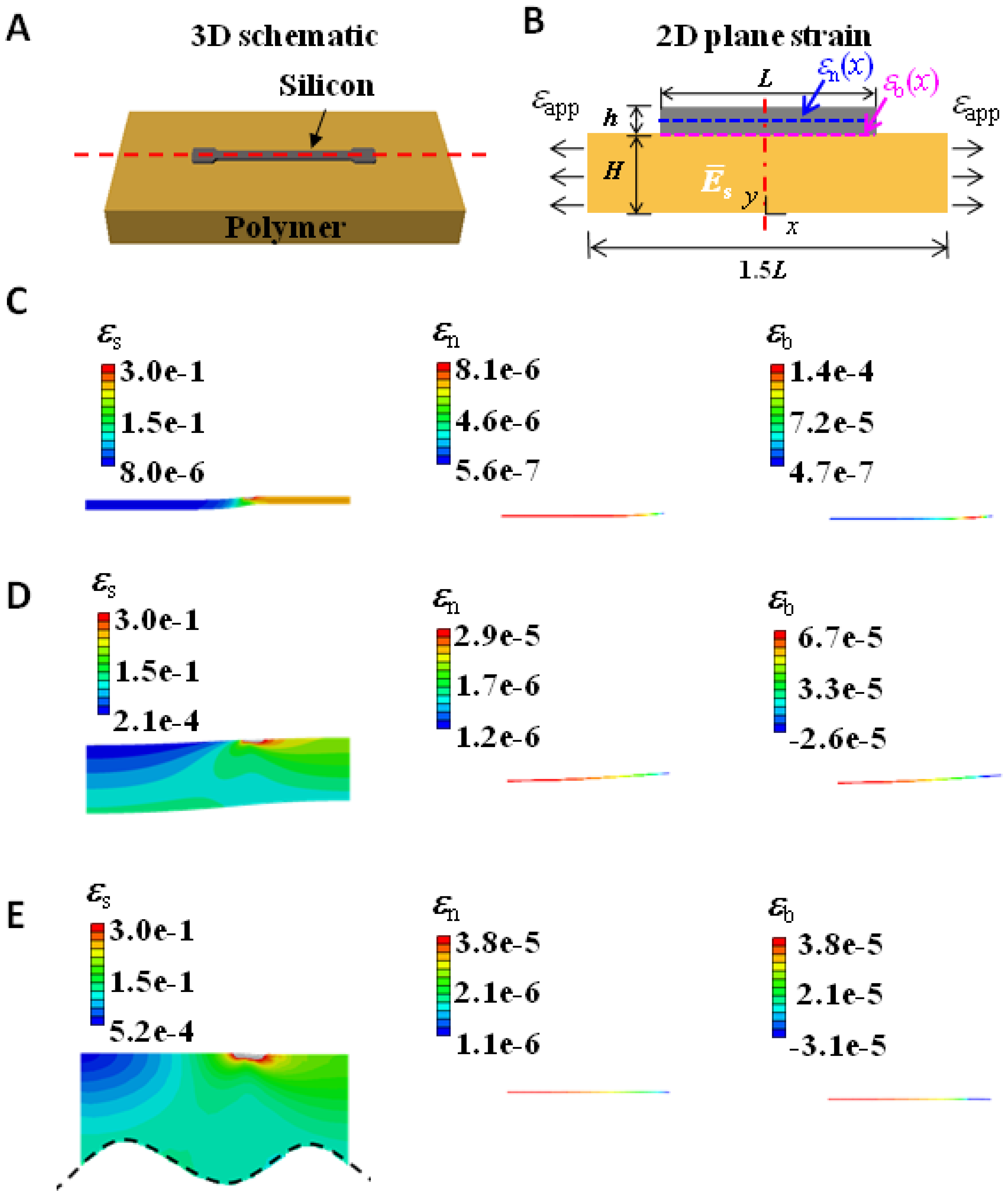
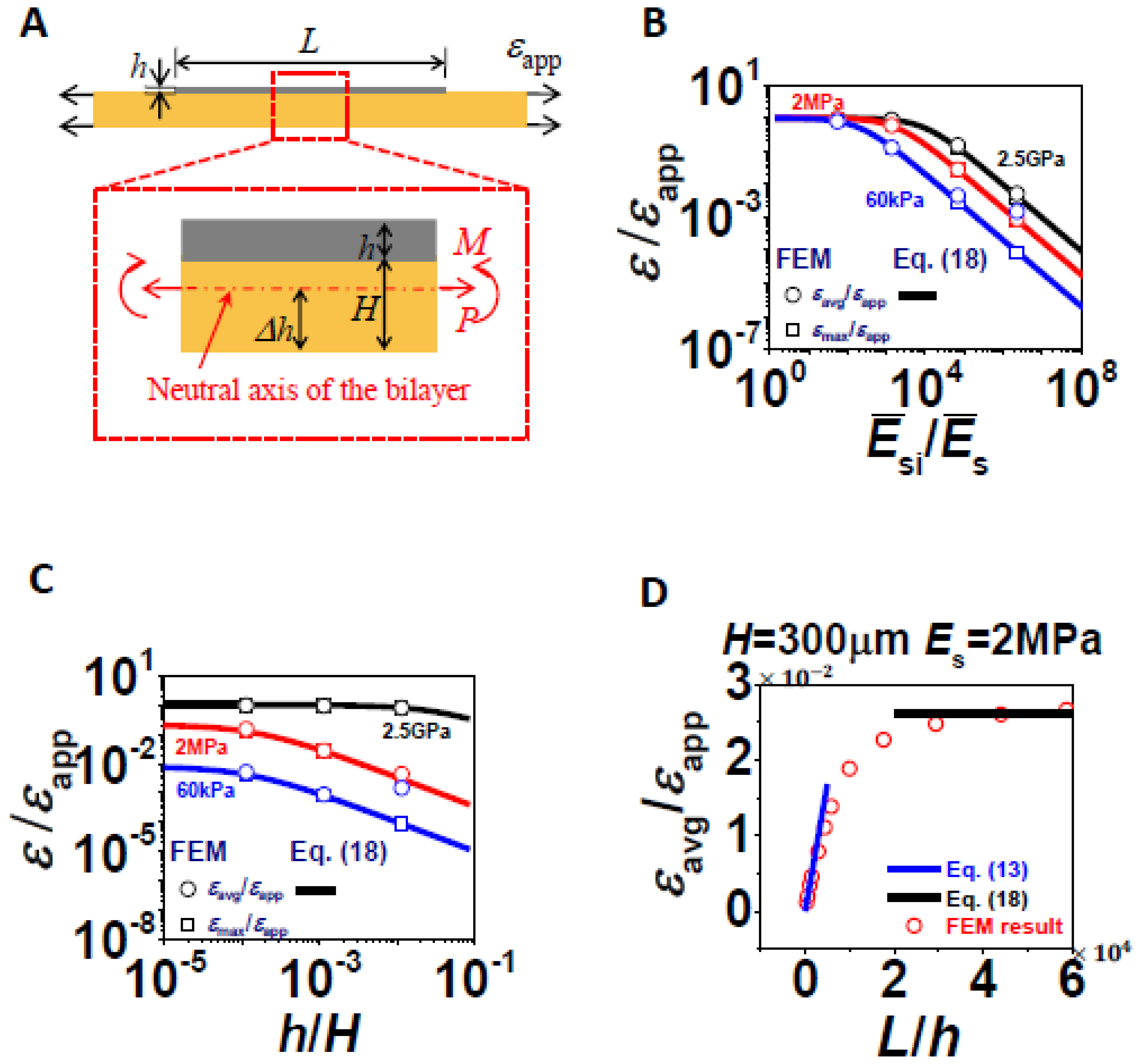
Silicon-based stretchable strain gauges are often composed of arrays of strips. The modeling work in this paper will just focus on a unit cell cut out of the periodic array. A schematic of a unit cell and its corresponding 2D plane strain model are depicted in Figure 1A,B. L represents the length of the silicon strip, h and H are the thicknesses of silicon and polymer, respectively. To minimize the number of variables, the size of the unit cell is fixed to be 1.5 L for all the models following a convention of island-on-polymer analysis [19–21]. When a uniform tensile strain, εapp, is applied to the substrate, the resistance of the silicon strip will change by ΔR, and the effective GF of the strain gauge system is defined as:
Although strain distribution in silicon might not be uniform, it has been proven [11] that the fractional change of resistance is proportional to the average longitudinal strain in silicon, i.e.:
Plugging Equation (3) into Equation (2) yields:
The maximum strain in silicon, εmax, will be related to the stretchability of the system. We define stretchability as the critical strain applied to the substrate, , beyond which silicon will rupture. For brittle silicon, we adopt a failure criterion, εmax = εcr, in which εmax represents the maximum tensile strain in silicon and εcr denotes the intrinsic critical strain-to-rupture of silicon that is to be measured experimentally. The failure criterion can be rewritten in the normalized form , which can be rearranged to obtain the stretchability:
When the polymer substrate is very thin or very soft, there will be slight concave bending in the silicon strip when the substrate is subject to tensile strain (Figure 1C,D). As a result, the maximum strain in silicon always takes place along the bottom of silicon. Using εb(x) to denote strain along the bottom of silicon as shown in Figure 1B, then:
As we have related the device performance indices, GF and stretchability, to εavg and εmax in silicon respectively, in the following we will calculate εavg and εmax to ultimately determine GF and stretchability. Through dimensional analysis, we can get
3. Finite Element Modeling
Over one hundred finite element models are built using commercial software package ABAQUS 6.11 to reveal the effect of the three variables in Equations (8) and (9). The boundary conditions and geometries are chosen to resemble the experimental setups when the sample is subject to uniaxial tension for GF calibration [9,13,14]. Because of symmetry, only the right half of the system shown in Figure 1B is modeled. A symmetric boundary condition is applied along the axis of symmetry, and the right end of the substrate is subject to a uniform horizontal displacement so that εapp is fixed to be 10% for all models. Nonlinear geometry analysis has to be enabled in ABAQUS because large deformation can be found in the portion of the polymer substrate that is not covered by silicon. Silicon thickness h is set to be 340 nm, the same thickness as the silicon nanomembrane used in most stretchable strain gauges [9,13,14]. Silicon length L varies from 10 μm to 20,000 μm and substrate thickness H varies from 30 μm to 3,000 μm, all are representative experimental parameters. The substrate length is set to be always 1.5 L for this unit cell. Perfect bonding is assumed between silicon and the substrate. Silicon and substrate are meshed using linear beam and plane-strain elements respectively. We model (110) silicon as a linear elastic material and polymer substrates as Neo-Hookean materials. Although the stress-strain curves for linear elastic and Neo-Hookean materials are not quite differentiable for strains up to 10%, we found the Neo-Hookean constitutive law is very helpful to achieve convergent solutions when nonlinear geometry analysis is enabled in ABAQUS. Effective materials properties in terms of Young's modulus and Poisson's ratio are listed in Table 1.
Representative contour plots of longitudinal strain in the substrate and in silicon are given in Figure 1C–E. They are from models with parameters L = 1,000 μm, Es = 60 kPa and H varying from 30 μm to 3,000 μm. When the substrate is stretched by 10%, strain in silicon is as small as 10−7 to 10−4, depending on substrate thickness. It is because silicon is six orders of magnitude stiffer than Ecoflex substrate (Es = 60 kPa) so that it is highly resistant to elongation, whereas the portion of the substrate not covered by silicon has to accommodate the applied strain by tensile strains up to 25%. Due to huge elastic mismatch between silicon and Ecoflex, horizontally applied tensile strain on a thin substrate will cause bending deformation in the silicon strip, especially near the end (Figure 1C,D). Therefore when the substrate is thin, the strain along the neutral axis of silicon, εn, is always smaller than the strain along the bottom of silicon, εb. Although εn is monotonic with x, εb might not be so due to localized bending near the end of the strip. When the substrate is thick enough (Figure 1E), it can be considered semi-infinite and hence can suppress the bending, resulting in identical εn and εb. Figure 1C–E only list FEM results for Es = 60 kPa, as the substrate becomes stiffer, the bending will be less significant.
3.1. Strain Distribution in Silicon
Figure 2 offers the distribution of εn and εb along x for different Es, L, and H.Figure 2A-C plot εn and Figure 2D-E plot εb. In all the plots, x = 0 represents the center of silicon and x = L/2 represents the right edge of silicon, as defined in Figure 1B. A generic feature of every strain distribution curve in Figure 2 is that strains always vanish at the traction free edge. Because of the traction free edge, the internal normal force of silicon at position x, i.e., ESihεn(x), has to balance the integration of interfacial shear stress from position x to the edge of silicon, L/2. As shown in Figure 2A-C, εn gradually builds up towards the center of silicon because interfacial shear force also builds up as we move away from the edge. The rate of strain growth decreases as x approaches the center of silicon because the interfacial shear stress decays from the edge to the center of silicon. If L is large enough, a plateau of maximum tensile strain could be reached toward the center of silicon. The distribution of εb shares some similarity with εn, as shown in Figure 2D-E. However, εb is not always monotonic with x. When the substrate is soft, e.g., Es = 60 kPa, edge bending can cause large variations in εb, as shown in Figure 2E,F.
To study one effect at a time, we first vary Es with L = 1,000 μm and H = 300 μm fixed. The distribution of εn and εb for different Es (60 kPa, 2 MPa, and 2.5 GPa) are plotted in Figure 2A,D, with vertical axis in logarithmic scales. A key observation is that both εn and εb increase as substrate modulus increases. It is simply because the stiffer substrate can apply higher shear stress to silicon, meaning that silicon can be stretched more by stiffer substrate. When substrate is very stiff, i.e., when Es = 2.5 GPa, there is little difference between εn and εb curves because the assembly will stay almost flat. But when Es = 60 kPa, εb are larger than εn due to slight global concave bending.
To study the effect of L, we fix H = 300 μm and Es = 60 kPa. The distribution of εn and εb for different L (200, 500, 1,000, 1,500, and 2,000 μm) are plotted in Figure 2B,E. The plateau values of both εn and εb increase as L increases because the longer L provides the longer distance for interfacial shear force (and hence the normal strain) to build up. Although εn monotonically decreases with increasing x, εb curves in Figure 2D always have some abnormal behaviors near the edge of silicon, as the result of highly localized curvature near the edge of silicon, as evident in Figure 1C-E.
To study the effect of H, we fix L = 1,000 μm and Es = 60 kPa and vary H from 30 μm to 3,000 μm in Figure 2C,F. Since thicker substrates provide stronger constraint to silicon, the plateau value of εn is higher when H is larger. The variation of εb is more complicated than εn because when substrate is soft (e.g., Es = 60 kPa in this case), bending strain could become very significant. Depending on substrate thickness, bending strain distribution also varies a lot. When H = 3,000 μm, there is very small bending curvature in the majority part of silicon (Figure 1E) and hence the plateau values of the black curves in Figure 2C,F are very similar. At the edge of silicon, localized concave bending induces compressive strain at the bottom of silicon because the neutral axis of the assembly is located somewhere within the substrate, hence a dip presents in the black curve of Figure 2F. When H = 300 μm, neutral axis locates within silicon, hence slight global concave bending (Figure 1D) will induce tensile strain along the bottom of silicon, resulting in elevated red curve in Figure 2F. Toward the edge of silicon, the neutral axis will gradually shift into the substrate and hence a dip also presents. When H = 30 μm, bending occurs almost exclusively at the edge (Figure 1C), hence the plateau values of the blue curves in Figure 2C,F are very similar. However, toward the edge of silicon, there is highly localized concave bending. Since neutral axis is within silicon, the bottom of silicon is subject to large tensile strain, resulting in a big bump in the blue curve of Figure 2F. As a conclusion, Figure 2 has demonstrated that unlike εn(x), εb(x) is not a monotonic function and the effect of H on it is not monotonic either. To find the maximum tensile strain, εmax, in silicon, we need to find the maximum positive values of each εb(x) curve, which does not necessarily occur at the center of silicon.
3.2. Average Strain and Maximum Strain
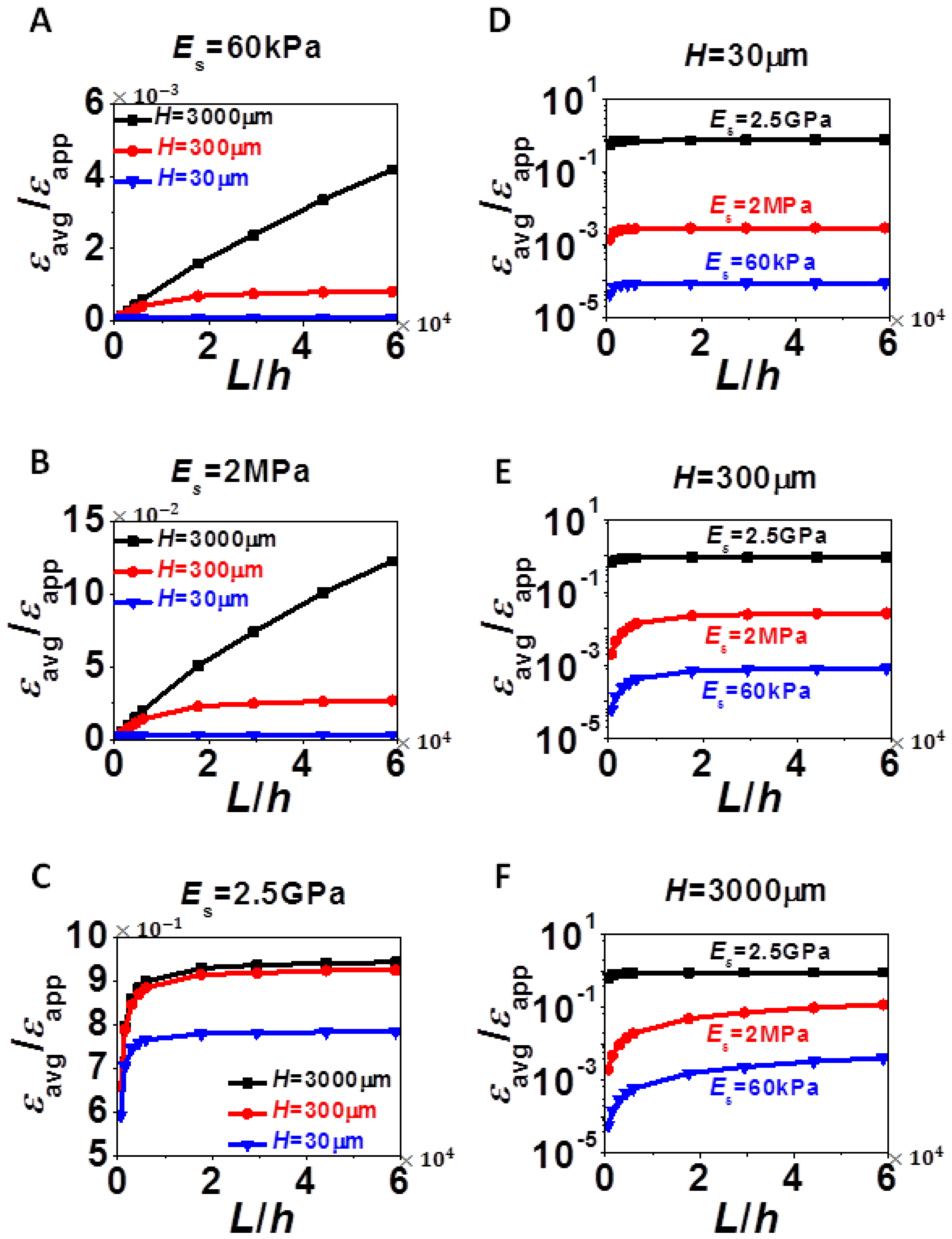
With the insights from strain distribution in Figure 2, Figures 3 and 4 investigate the effect of the three variables L, H, and Es, on the average strain (εavg) and the maximum strain (εmax) in silicon. Average strains are calculated from averaging the values of εn (Equation (4)) and maximum strains are determined through finding the maximum positive values of εb (Equation (7)). Figure 3 plots normalized εavg as a function of L/h. The same set of data is presented in two different ways: each plot in Figure 3A-C has a fixed Es and varying H whereas each plot of Figure 3D-F has a fixed H and varying Es. All plots in Figure 3 show that εavg increases with increased film size (L), substrate thickness (H) and substrate modulus (Es), all of which imply the stronger constraint the substrate is able to apply to silicon, the higher εavg. Due to experimental limitations on L and H, changing Es would be the most effective way to tune εavg, by orders of magnitude. According to Figure 3A-C, it is interesting to notice that when L is very small, especially compared to H, there exists a linear relation between εavg and L. According to Figure 3D-F, it is also easy to discover that when L is large enough, εavg will always reach a plateau, i.e., εavg becomes independent of L, and the smaller the H, the faster the plateau can be reached. We will thereby consider the limiting cases of L/H ≪ 1 and L/H ≫ 1 and try to derive analytical solutions for εavg in Section 4.
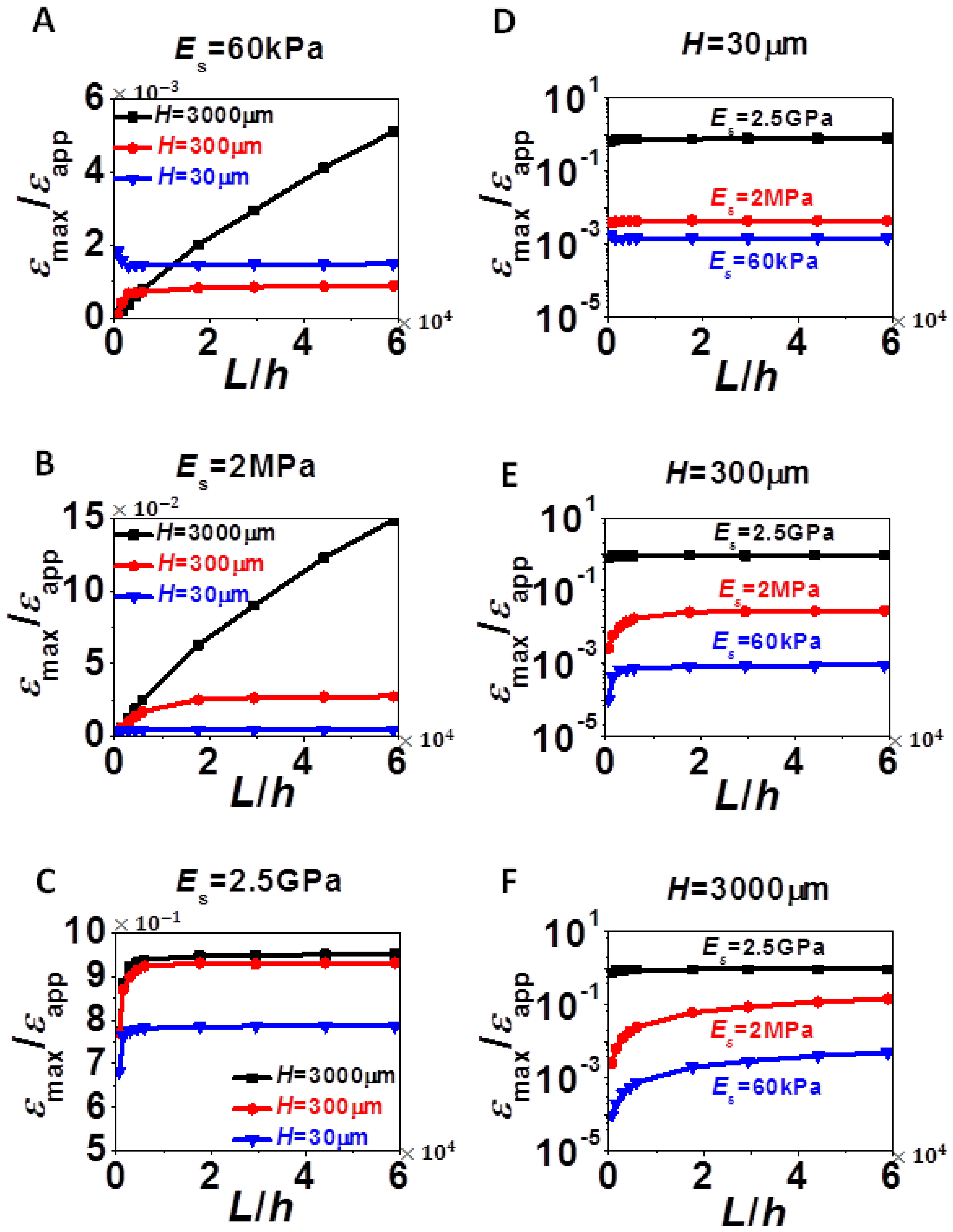
Figure 4 plots the normalized εmax as a function of L/H for various H and Es in a format similar to Figure 3. Each plot in Figure 4A-C has a fixed Es and varying H whereas each plot of Figure 4D-F has a fixed H and varying Es.
The difference between εmax and εavg is that εmax has extra bending contribution. Therefore, similar to εavg, εmax always increases with increased L and Es, and with increased H in most cases. However, when the substrate is very compliant and when L is small, Figure 4A shows that εmax could be higher in thinner substrate due to localized bending effect we discussed for Figure 2F. As Es increases to 2.5 GPa, as shown in Figure 4C, bending effect is almost negligible and hence εmax and εavg become undistinguishable, i.e., Figures 3C and 4C look identical. Similar conclusions can be applied to thick substrate (H = 3,000 μm) when comparing Figures 3F and 4F. For the two limiting cases, L/H ≪ 1 and L/H ≫ 1, we also observed similar features as in Figure 3, i.e., linear when L/H ≪ 1 and plateau when L/H ≫ 1. Hence analytical solutions of εmax will be derived in Section 4 as well.
4. Analytical Modeling
In this section, we are going to develop analytical models for two limiting cases: L/H ≪ 1 and L/H ≫ 1, and the analytical solutions will be compared with the FEM results.
4.1. When L/H ≪ 1
When L/H ≪ 1, h/H ≪ 1 is also true since experimentally L > h is always valid. In this case, H is no longer a relevant variable in the system and the substrate can be considered infinitely thick. Hence εavg and εmax only depend on Ēs/ĒSi and L/h, and Equation (8) degenerates to:
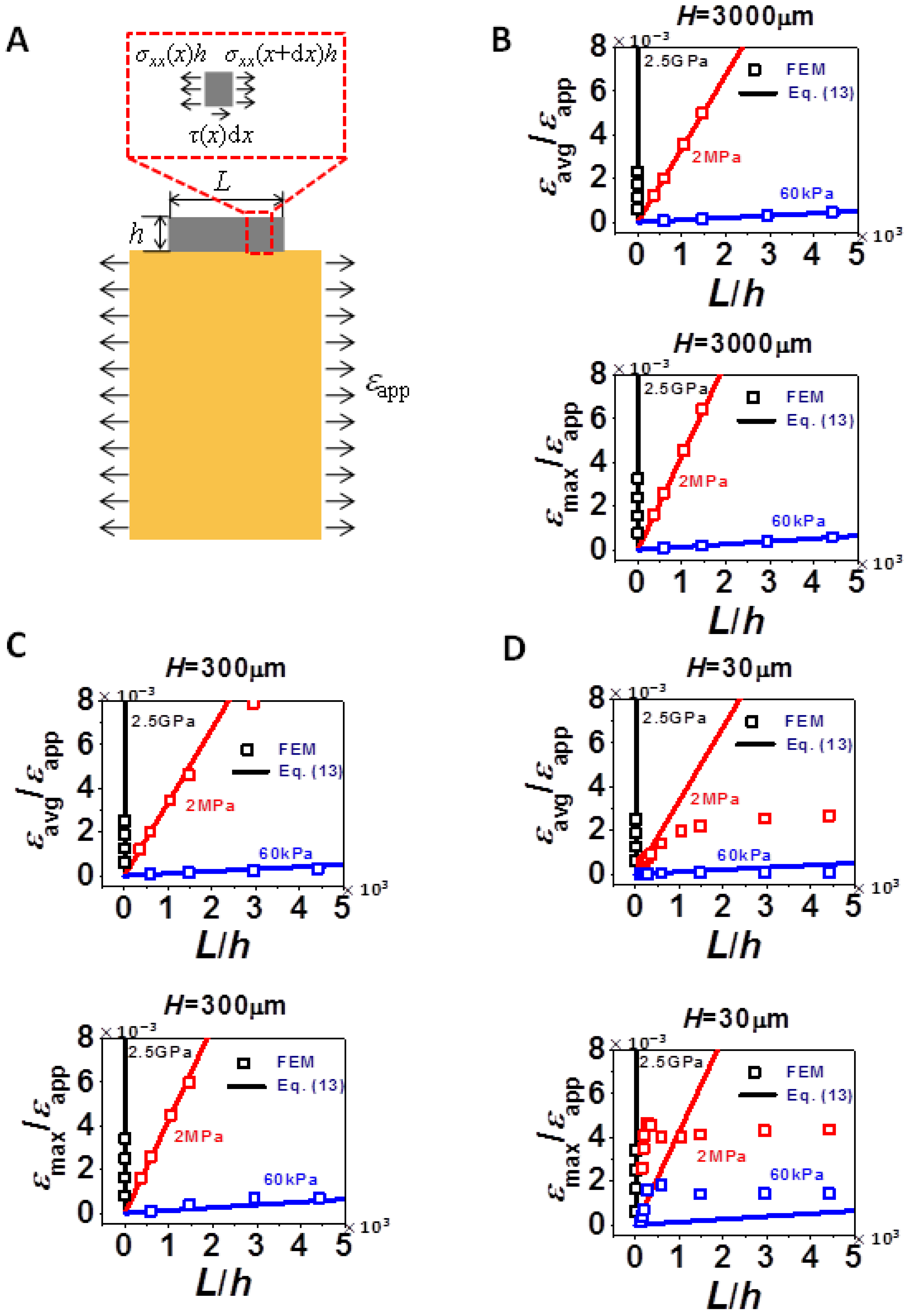
To determine the f function, a shear lag model is adopted as shown in Figure 5A. The free body diagram (FBD) of a thin slice of silicon would give the following equilibrium equation:
In conclusion, when L/H ≪ 1, average and maximum strains in silicon scale linearly with Ēs and L. Since Ēs can be easily changed by orders of magnitude as shown in Table 1, strains in silicon could also be tuned cross wide ranges.
4.2. When L/H ≫ 1
When L/H ≫ 1, assuming L/H ≫ 1 is always valid, relevant variables reduce to ĒSi/Ēs and h/H. To derive analytical solution for this case, we make two cross-sectional cuts within the length of silicon and the FBD is shown in Figure 6A. The neutral axis of this bilayer is given by [29]:
Boundary conditions are decomposed to P and M, which are both acting at the neutral axis. Assuming the following relation between P and εapp:
Following this practice, the simplest form of average strain in silicon can be written as:
Combining Equations (15)–(17) gives:
Through curve fitting of FEM results, a and b can be obtained as a = 5.46 × 10⁻⁵ and b = 0.428. Equation (18) turned out to be an universal expression to capture εavg/εapp and εmax/εapp, over wide ranges of Σ and η provided L ≫ H. For very big Σ and η, i.e., very compliant and thin substrate, Equation (18) cannot capture εmax/εapp very well due to localized bending effects.
Figure 6B,C plots Equation (18) (as curves) against FEM results (as markers) in log log scale. Some important conclusions can be drawn and rationalized from the two plots. First, when the substrate is as stiff as silicon, or when the substrate is infinitely thick, ε/εapp approaches 1. When the substrate becomes extremely soft or extremely thin, ε/εapp can be reduced by orders of magnitude, and should eventually die out. Figure 6C also tells that the effect of h/H is insignificant when the substrate is very stiff but gradually becomes more effective as the substrate modulus reduces.
With the two semi-analytical solutions given by Equations (13) and (18), it is useful to plot them for a representative combination of (Σ, η) in a L/H plot as shown in Figure 6(D). It is clear that Equations (13) and (18) can successfully bond the FEM results, except the transition zone.
5. Tradeoff between Gauge Factor and Stretchability
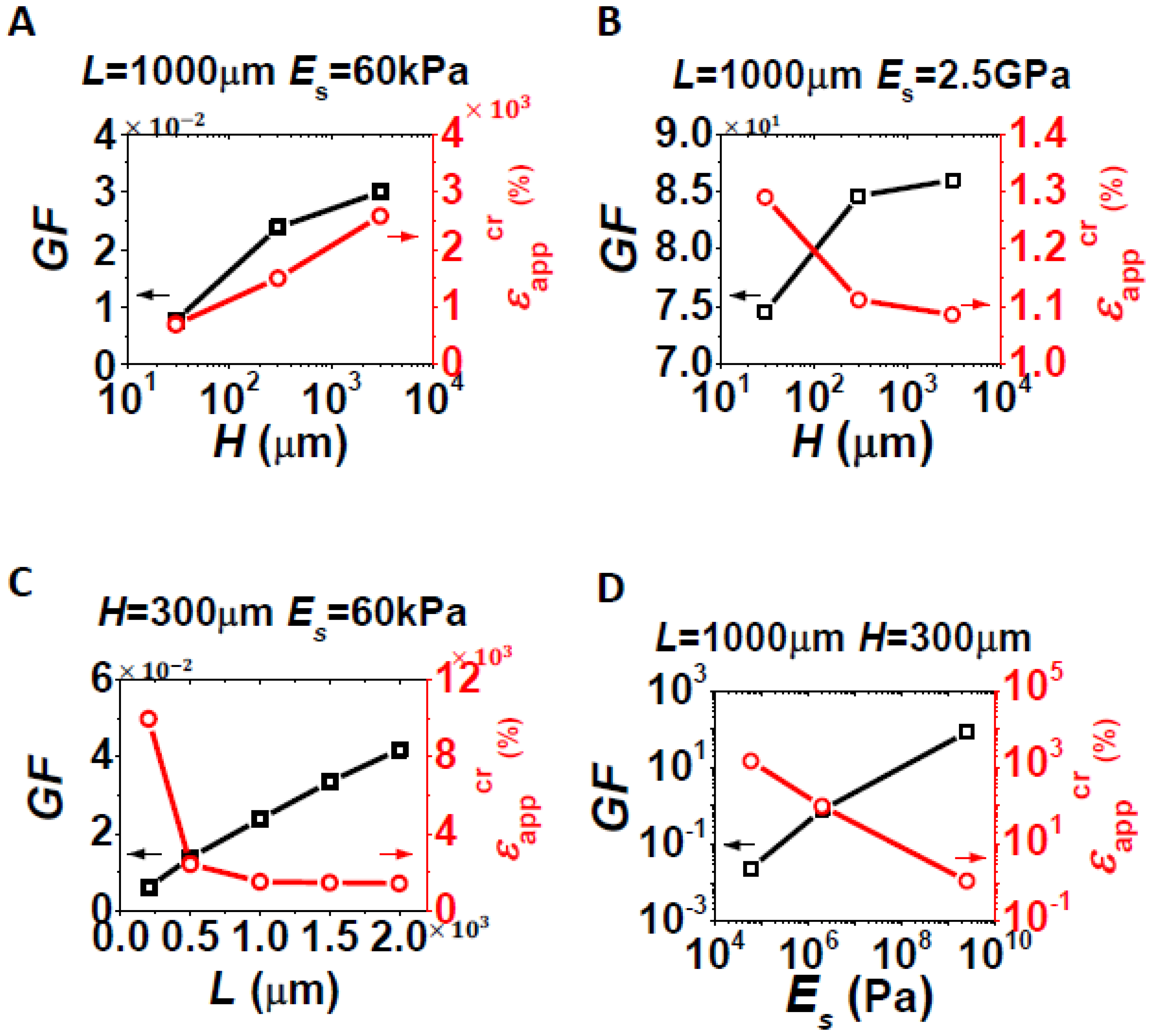
After finding out εavg/εapp and εmax/εapp, the final step is to use Equations (5) and (6) to determine the gauge factor, GF, and the stretchability, , of a particular strain gauge. For the purpose of illustration, we have to assume some reasonable numbers for the intrinsic properties for silicon, including GFSi = 100 [9] and εcr = 1%. Some representative results are shown in Figure 7, with GF in black and in red in each plot. First, effects of H are studied for fixed L, and Es, as shown in Figure 7A,B. Comparing the two plots, GF always increases as H increases, but the variation of with H depends on Es. When the substrate is really soft and silicon is short, as the case for Figure 7A, the assembly is easy to bend especially when H is small. The local bending induced strain contributes significantly to εmax which is inversely proportional to according to Equation (6). As a result, thinner substrate induces higher maximum strain and hence lower stretchability. When the substrate is stiff, e.g., Es = 2.5 GPa as shown in Figure 7B, there is almost no bending in the assembly and hence the thicker substrate induces higher maximum strain (Figure 4C). It is interpreted as a tradeoff between stretchability and GF. As constraints from the substrate become stronger, i.e., as L, H, or Es increases, the larger strain in silicon suggests the higher GF but the lower stretchability, which has been confirmed by Figure 7C,D. Effects of L are studied for fixed H and Es, as shown in Figure 7C. For longer strip, the GF is larger but the stretchability is lower. This is always the case for other H and Es combinations. Similar effects are observed for Es, as shown in Figure 7D, except that the scales of both GF and are in log scale, suggesting a big tuning range. For example, when Es = 60 kPa, the critical applied strain to rupture silicon can be as high as 10,000% in theory, which implies that the stretchability of the strain gauge is only limited by the stretchability of the substrate. But it corresponds to a GF as low as 0.006. Practically, GF should be at least 1 for strain measurement, which implies Es should be 2 MPa and beyond, which still corresponds to stretchability beyond 100%.
The goal of plots in Figure 7 is to provide guidance for engineers to choose the right strain gauge systems under certain constraints or to predict the performance of a given stretchable strain gauge based on silicon nanomembrane. For example, to measure an object which deforms up to 30%, we will need to choose experimentally appropriate L, H, and Es to make a strain gauge with a stretchability of 30% and maximized GF. Since the effects of L and H are within one order of magnitude as shown in Figure 7A–C, we could fix them at reasonable numbers and the key is to select the right stiffness for the substrate, using a plot as shown in Figure 7D. A stretchability of 30% corresponds to a Es = 1.1 × 10⁷ Pa, which in turn predicts the GF to be 3.27.
We have three final remarks on applying the analysis in this paper to real strain gauge samples [9,13,14]. In real samples, brittle silicon strip is usually sandwiched between two layers of insulating polyimide, and the strip is connected to metallic interconnects (usually in serpentine shape) for data acquisition. Laminating insulating polymers on silicon strip is equivalent to an increase of h, which would decrease strain in silicon and hence decrease the system GF. Adding interconnects to silicon is equivalent to an increase of L, which would increase strain in silicon and hence increase the system GF. Therefore the idealized model in Figure 1B may not offer the most accurate quantitative prediction for a practical sample. But we can always run 3D FEM to calculate the strain in silicon taking into account the actual layout of the circuits and the multilayer lamination to predict a pertinent GF and stretchability for that specific strain gauge system.
The coupling between tension and bending is a generic problem associated with mechanical strain gauges. This study has also shed light on this issue. When Es ≪ ESi, the neutral axis of the bilayer almost overlaps with the neutral axis of silicon. In this case bending will induce minimum εavg in silicon and hence bending effect can be neglected. When Es is close to ESi, the neutral axis of the bilayer lies far away from the neutral axis of silicon. In this case the bending will induce large εavg in silicon. To minimize the bending induced signal when the substrate is a stiff polymer, one can add an identical polymer layer on top of silicon, forming a sandwiched structure to locate silicon along the neutral axis of the sandwich structure. This structure can be readily analyzed by replacing the old H with the new 2H, leaving everything else unchanged.
Due to the mismatch in coefficients of thermal expansion (CTE) between silicon and polymer, temperature variation will induce stress and hence resistance change in silicon. The best known method to eliminate temperature effect is to use Wheatstone bridge instead of single resistors. The mechanical analysis on a single resistor offered in this paper is readily applicable to each linear arm of the Wheatstone bridge.
6. Conclusions
In conclusion, we performed strain analysis on polymer-bonded thin silicon strips using both FEM and analytical methods. The gauge factor and stretchability of a silicon-on-polymer strain gauge have been predicted as functions of the normalized length of silicon, and the normalized thickness and modulus of the polymer substrate. In general, we found that the longer strip, the thicker or the stiffer substrate will transfer a larger fraction of the applied strain to silicon. Silicon length and substrate thickness has only moderate effects on strain in silicon whereas varying the stiffness of the substrate could change the strain and hence the gauge factor and stretchability by orders of magnitude. A tradeoff between GF and stretchability has been discovered. Since wide ranges of gauge factor and stretchability can be achieved through tuning the substrate modulus, results from this work can be used as guidelines to design appropriate strain gauges or to predict the performance of fabricated strain gauges.
Acknowledgments
This work is supported by the start-up fund provided by the Cockrell School of Engineering at the University of Texas at Austin.
Conflict of Interest
The authors declare no conflict of interest.
References
- Window, A.L. Strain Gauge Technology; Elsevier Applied Science: London, UK, 1992. [Google Scholar]
- Lu, N.S.; Wang, X.; Suo, Z.G.; Vlassak, J. Metal films on polymer substrates stretched beyond 50%. Appl. Phys. Lett. 2007, 91. [Google Scholar] [CrossRef]
- Smith, C.S. Piezoresistance effect in germanium and silicon. Phys. Rev. 1954, 94, 42–49. [Google Scholar]
- Sze, S.M. Semiconductor Sensors; Wiley: New York, NY, USA, 1994. [Google Scholar]
- Barlian, A.A.; Park, W.T.; Mallon, J.R.; Rastegar, A.J.; Pruitt, B.L. Review: Semiconductor piezoresistance for microsystems. IEEE Proc. 2009, 97, 513–552. [Google Scholar]
- Kanda, Y. Piezoresistance effect of silicon. Sens. Actuators A Phys. 1991, 28, 83–91. [Google Scholar]
- Middelhoek, S. Silicon Sensors; Delft University: Delft, The Netherlands, 1994. [Google Scholar]
- Apanius, C.; Estrada, H.V.; Nagy, M.L.; Siekkinen, J.W. A User-Friendly, High-Sensitivity Strain Gauge. Available online: http://www.sensorsmag.com/sensors/force-strain-load-torque/a-user-friendly-high-sensitivity-strain-gauge-1091 (accessed on 4 June 2013).
- Won, S.M.; Kim, H.S.; Lu, N.S.; Kim, D.G.; del Solar, C.; Duenas, T.; Ameen, A.; Rogers, J.A. Piezoresistive strain sensors and multiplexed arrays using assemblies of single-crystalline silicon nanoribbons on plastic substrates. IEEE Trans. Electron. Devices 2011, 58, 4074–4078. [Google Scholar]
- Leonardi, M.; Pitchon, E.M.; Bertsch, A.; Renaud, P.; Mermoud, A. Wireless contact lens sensor for intraocular pressure monitoring: Assessment on enucleated pig eyes. Acta Ophthalmol. 2009, 87, 433–437. [Google Scholar]
- Lu, N.; Lu, C.; Yang, S.; Rogers, J. Highly sensitive skin-mountable strain gauges based entirely on elastomers. Adv. Funct. Mater. 2012, 22, 4044–4050. [Google Scholar]
- Yamada, T.; Hayamizu, Y.; Yamamoto, Y.; Yomogida, Y.; Izadi-Najafabadi, A.; Futaba, D.N.; Hata, K. A stretchable carbon nanotube strain sensor for human-motion detection. Nat. Nanotechnol. 2011, 6, 296–301. [Google Scholar]
- Ying, M.; Bonifas, A.P.; Lu, N.S.; Su, Y.W.; Li, R.; Cheng, H.Y.; Ameen, A.; Huang, Y.G.; Rogers, J.A. Silicon nanomembranes for fingertip electronics. Nanotechnology 2012, 23. [Google Scholar] [CrossRef]
- Kim, D.; Ghaffari, R.; Lu, N.; Wang, S.; Lee, S.P.; Keum, H.; D'Angelo, R.; Klinker, L.; Su, Y.; Lu, C.; et al. Electronic sensor and actuator webs for large-area complex geometry cardiac mapping and therapy. Proc. Natl. Acad. Sci. USA 2012, 109, 19910–19915. [Google Scholar]
- Liu, C. Recent developments in polymer MEMS. Adv. Mater. 2007, 19, 3783–3790. [Google Scholar]
- Dharap, P.; Li, Z.L.; Nagarajaiah, S.; Barrera, E.V. Nanotube film based on single-wall carbon nanotubes for strain sensing. Nanotechnology 2004, 15, 379–382. [Google Scholar]
- Sakhaee-Pour, A.; Ahmadian, M.T.; Vafai, A. Potential application of single-layered graphene sheet as strain sensor. Solid State Commun. 2008, 147, 336–340. [Google Scholar]
- Rogers, J.A.; Lagally, M.G.; Nuzzo, R.G. Synthesis, assembly and applications of semiconductor nanomembranes. Nature 2011, 477, 45–53. [Google Scholar]
- Lu, N.S.; Yoon, J.I.; Suo, Z.G. Delamination of stiff islands patterned on stretchable substrates. Int. J. Mater. Res. 2007, 98, 717–722. [Google Scholar]
- Yoon, J.; Zhang, Z.; Lu, N.S.; Suo, Z.G. The effect of coating in increasing the critical size of islands on a compliant substrate. Appl. Phys. Lett. 2007, 90. [Google Scholar] [CrossRef]
- Sun, J.Y.; Lu, N.S.; Yoon, J.; Oh, K.H.; Suo, Z.G.; Vlassak, J.J. Inorganic islands on a highly stretchable polyimide substrate. J. Mater. Res. 2009, 24, 3338–3342. [Google Scholar]
- Liu, C. Foundations of MEMS; Prentice-Hall: Englewood Cliffs, NJ, USA, 2006. [Google Scholar]
- Xia, Z.C.; Hutchinson, J.W. Crack patterns in thin films. J. Mech. Phys. Solids 2000, 48, 1107–1131. [Google Scholar]
- Handge, U.A. Analysis of a shear-lag model with nonlinear elastic stress transfer for sequential cracking of polymer coatings. J. Mater. Sci. 2002, 37, 4775–4782. [Google Scholar]
- Hopcroft, M.A.; Nix, W.D.; Kenny, T.W. What is the young's modulus of silicon? J. Microelectromechanical Syst. 2010, 19, 229–238. [Google Scholar]
- Kim, D.H.; Lu, N.S.; Ma, R.; Kim, Y.S.; Kim, R.H.; Wang, S.D.; Wu, J.; Won, S.M.; Tao, H.; Islam, A.; et al. Epidermal electronics. Science 2011, 333, 838–843. [Google Scholar]
- Fuard, D.; Tzvetkova-Chevolleau, T.; Decossas, S.; Tracqui, P.; Schiavone, P. Optimization of poly-di-methyl-siloxane (PDMS) substrates for studying cellular adhesion and motility. Microelectron. Eng. 2008, 85, 1289–1293. [Google Scholar]
- DuPont™ Kapton® HN Polyimide Film Technical Data Sheet. Available online: http://www2.dupont.com/Kapton/en_US./downloads/pdf/HN_datasheet.pdf (accessed on 4 June 2013).
- Hutchinson, J.W.; Suo, Z. Mixed-mode cracking in layered materials. Adv. Appl. Mech. 1992, 29, 63–191. [Google Scholar]


© 2013 by the authors; licensee MDPI, Basel, Switzerland. This article is an open access article distributed under the terms and conditions of the Creative Commons Attribution license (http://creativecommons.org/licenses/by/3.0/).
Share and Cite
Yang, S.; Lu, N. Gauge Factor and Stretchability of Silicon-on-Polymer Strain Gauges. Sensors 2013, 13, 8577-8594. https://doi.org/10.3390/s130708577
Yang S, Lu N. Gauge Factor and Stretchability of Silicon-on-Polymer Strain Gauges. Sensors. 2013; 13(7):8577-8594. https://doi.org/10.3390/s130708577
Chicago/Turabian StyleYang, Shixuan, and Nanshu Lu. 2013. "Gauge Factor and Stretchability of Silicon-on-Polymer Strain Gauges" Sensors 13, no. 7: 8577-8594. https://doi.org/10.3390/s130708577