Influence of Conductivity and Dielectric Constant of Water–Dioxane Mixtures on the Electrical Response of SiNW-Based FETs

Abstract
: In this study, we report on the electrical response of top-down, p-type silicon nanowire field-effect transistors exposed to water and mixtures of water and dioxane. First, the capacitive coupling of the back gate and the liquid gate via an Ag/AgCl electrode were compared in water. It was found that for liquid gating smaller potentials are needed to obtain similar responses of the nanowire compared to back gating. In the case of back gating, the applied potential couples through the buried oxide layer, indicating that the associated capacitance dominates all other capacitances involved during this mode of operation. Next, the devices were exposed to mixtures of water and dioxane to study the effect of these mixtures on the device characteristics, including the threshold voltage (VT). The VT dependency on the mixture composition was found to be related to the decreased dissociation of the surface silanol groups and the conductivity of the mixture used. This latter was confirmed by experiments with constant conductivity and varying water–dioxane mixtures.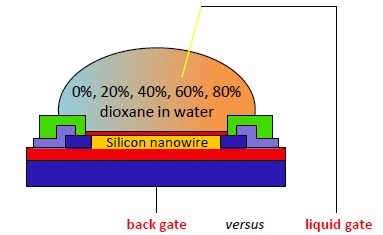
1. Introduction
Silicon-based nanowire devices have been the subject of extensive research in the last decade. Most of the work focuses on different aspects of device fabrication and on (potential) sensor applications for the label-free detection of (bio)chemical species [1–4]. Studies on (bio)chemical sensing typically require (bio)chemical modification of the nanowire surface [5]. In addition, there is a large series of studies on the description of fundamental performance limits of nanowire-based devices [6,7], charge screening effects [8–10], improvement of the signal-to-noise ratio [11–13], the effect of surface modification on the nanowire electrical properties [14,15], and work on the incorporation of a reference electrode [16,17].
Soon after their introduction in 2001 [18], devices based on silicon nanowires (SiNWs) were applied in sensing experiments, addressing the pH sensitivity of silicon oxide-covered SiNWs as well as the detection of streptavidin binding on biotin-modified nanowires. The sensing mechanism was rationalized by considering the type of doping present in the SiNW and the changes in charge density at the sensor interface. The surface potential as a result of the surface charge density offsets the front and/or back gate potential and leads to a change of majority charge carriers in the SiNW. By far, most of the studied target compounds are charged and studied in an aqueous environment. Examples include not only protons and antibodies/antigens [18], but also deoxyribonucleic acid (DNA) [15,19], polyelectrolytes [20] and ions [21]. Recently it was shown that the response of so-called nanoISFET pH sensors can be described by analytical models [22], similar to those developed for describing the operation of ISFETs [23].
Since 2007 the responses of SiNW-based devices—which behave like field-effect transistors (FETs)—to uncharged target species in the gas or vapour phase have also been studied. This was first shown by Heath and his co-workers who studied the exposure of NO2, acetone and hexane in nitrogen (N2) to bare and silane-modified SiNWs [24]. Later, Engel et al. prepared aminopropyl-terminated SiNWs to detect trinitrotoluene (TNT) in N2 [25]. Over the past few years, Haick and co-workers reported an interesting series of research papers on the fundamentals and applications of functionalized SiNW-based FETs for the detection of polar (water, ethanol, 1-butanol, 1-hexanol, 1-octanol and 1-decanol) and nonpolar (n-hexane, n octane and n-decane) volatile organic compounds (VOCs) in oil-free air having 15% relative humidity [26–31]. This in-depth work shows that one of the sensing mechanisms involved is related to the changes in the surrounding dielectric medium due to the condensation of VOCs on the functionalized SiNW surface [29]. The surrounding dielectric effect is also believed to play a role in an interesting contribution of the Nokia Research Center in which etched SiNW-based devices were exposed to (neat) vapours of water, acetone, methanol, ethanol and 2-propanol in air [32].
In the present study we investigated the effect of exposure of the SiNWs to different solvents and the dielectric coupling in more detail. We used well-defined, top-down prepared, p-type SiNW-based devices. The SiNWs were covered with SiO2 and were not further modified. Their electrical response to binary, liquid mixtures of water and dioxane, having a range of dielectric constants (εr varies between 2 and 80), was studied. In contrast to the detection of vapours or gases described in the previous paragraph, the analysis of the FET responses in the liquid environment, allows one to apply liquid gating (i.e., front gating) next to back gating. In this article we compared and discussed the influence of type of gating in aqueous solutions. Several papers have discussed the use of back gating and methods for liquid gating (e.g., on-chip Au and Pt electrodes, Ag/AgCl electrodes, extended off-chip gates [33–35]), but a direct comparison on the influence of the type of gating on the ID-VGS-characteristics has not been made before. Next, the devices were exposed to two different types of water–dioxane mixtures: as-prepared and mixtures with a constant electrical conductivity achieved by the controlled addition of a salt. The electrical characteristics of the devices when exposed to these conditions were investigated and discussed.
2. Experimental Section
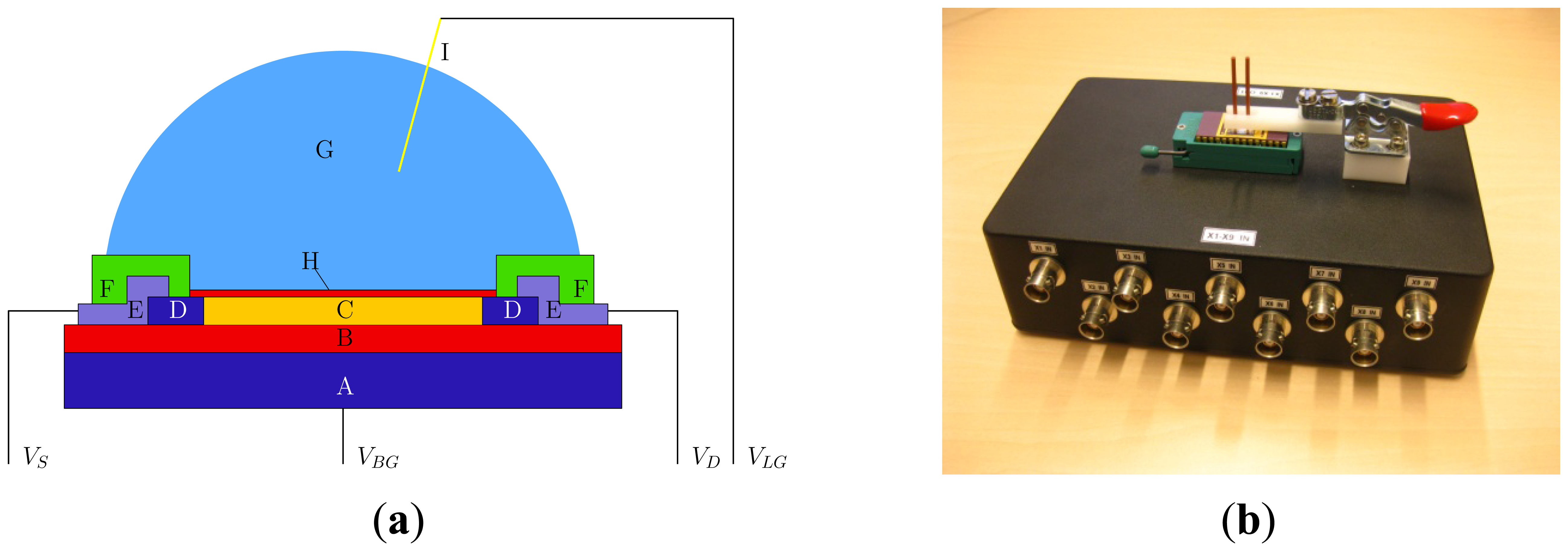
SiNW-FETs were produced as reported previously [36]. Briefly, the nanowires (p-doped at a concentration of 1016 cm−3 to assure semiconducting behaviour) are 3 μm in length, 300 nm in width and 40 nm in height and are covered with a silicon dioxide gate oxide with a thickness of 8 nm. The thickness of the buried oxide (BOX) layer is 300 nm. The devices were wire bonded and covered with a micro fluidic device. The setup is shown in Figure 1.
In order to investigate the difference between the use of a back gate (BG) and a liquid gate (LG), a Ag/AgCl electrode was inserted in the beaker containing the solution to which the nanowire was exposed. The solutions were sucked into the microfluidic cell with a syringe pump (Harvard Apparatus, Holliston, MA, USA) using Silastic® Q7-4750 tubing (Dow Corning, Midland, MI, USA). The devices were exposed to the solutions in a random order. The target solution was sucked from the beaker into the microfluidic cell after which the flow was stopped and the measurements were performed under stagnant conditions at room temperature. The measurement was started immediately after exposure to the liquid. Each exposure continued for approximately 10 min using the liquid gate as described previously.
A standard Keithley 4200 semiconductor characterization system (Keithley Instruments BV, Gorinchem, The Netherlands) equipped with eight source measurement units was used for the electrical characterization of the device during exposure. A 50 mV source-drain bias was applied and VGS was applied such that the device is operated in depletion mode in the linear regime (VSD ≪ VGS). The drain current (ID) was measured while the gate potential (VGS) was swept. This can be applied either via the back gate or the liquid gate. From these characteristics the threshold voltage (VT) was determined.
To study the influence of the liquid medium in contact with the SiNW on the device characteristics 1,4-dioxane (anhydrous, 99.8%, Sigma-Aldrich Chemie B.V., Zwijndrecht, The Netherlands) (εr = 2.25) and de-ionized water (εr = 80.1; ρ = ∼20 kΩ cm) were used as solvent because they mix in all ratios and make it possible to change the dielectric constant gradually in the range of 2–80. They were mixed as described by Åkerlöf et al. [37] to obtain mixtures with a range of dielectric constants. To adjust the electrical conductivity, tetramethylammonium chloride (≥98%, Sigma-Aldrich Chemie B.V., Zwijndrecht, The Netherlands) was dissolved in the solvent mixtures where mentioned. The conductivity and pH of the solutions were measured using a Metrohm 712 Conductometer and a Metrohm 827 pH lab meter, respectively (Metrohm equipment was purchased from Applikon Analytical B.V., Schiedam, The Netherlands).
3. Results and Discussion
First the devices were exposed to water and the electrical characteristics were determined using the back gate and the liquid gate. The results of this comparison are discussed in Section 3.1. Subsequently, the devices were exposed to water–dioxane mixtures with a range of dielectric constants and the electrical characteristics were determined using liquid gating via an Ag/AgCl electrode (Section 3.2). In addition, the conductivity of some mixtures was adjusted to obtain solutions with similar conductivities.
3.1. Back Gate vs. Liquid Gate in De-Ionized Water
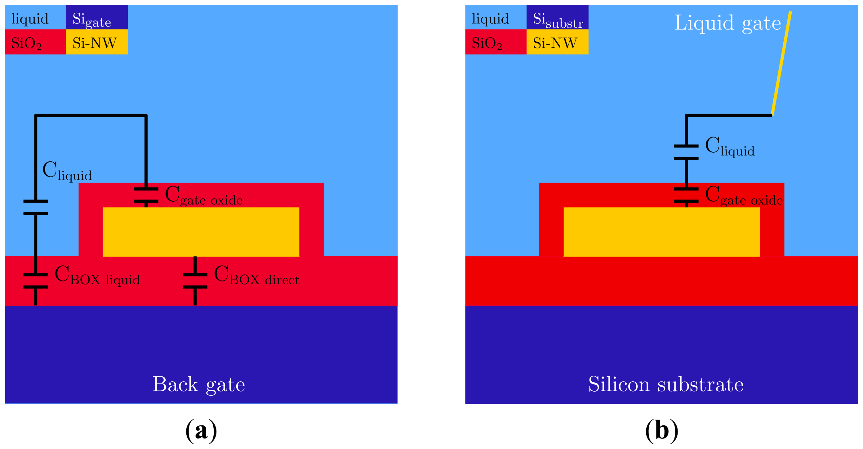
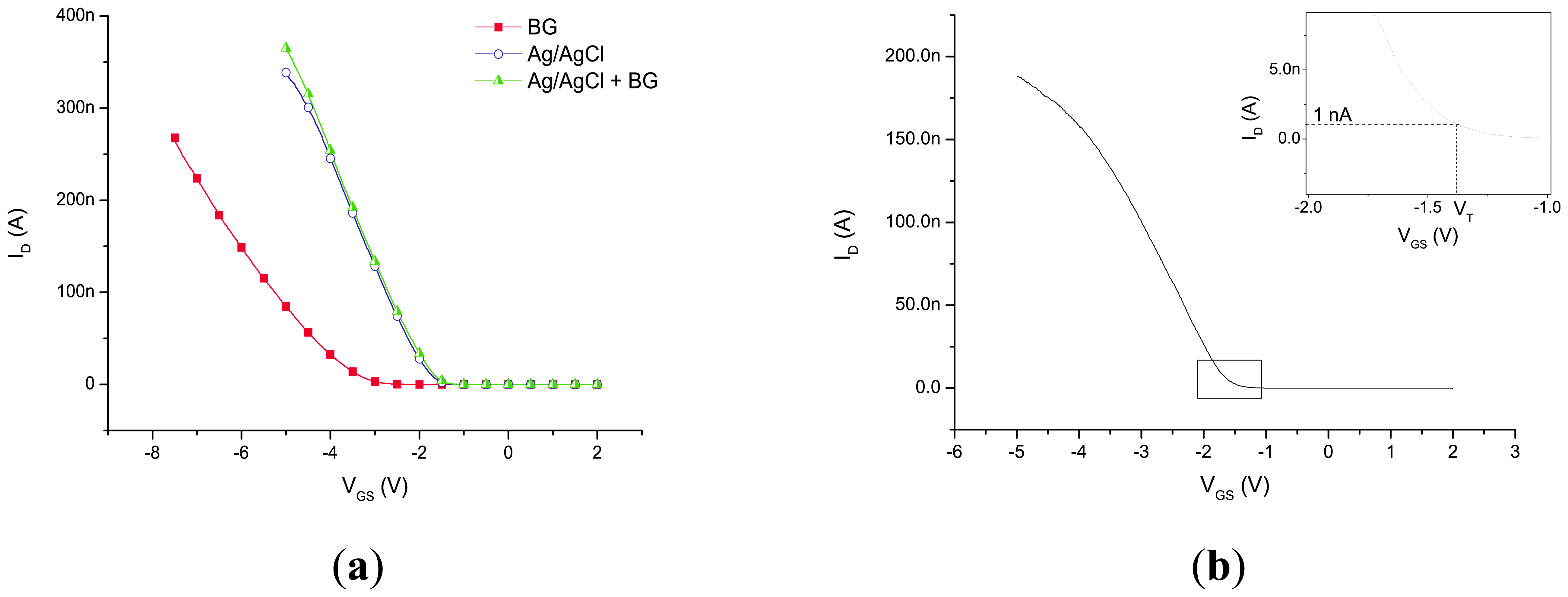
Figure 2 shows a schematic representation of the back-gated and liquid-gated situation and the capacitances that are present. In both cases the Cliquid was present, although it has a different value for the two cases, while Cbox only plays a role in the case of back gating. The ID-VGS characteristics that were obtained using three different types of modes of operation are given in Figure 3a: (1) the back gate was swept while no electrode is inserted in the solution; (2) the gate potential was applied via the Ag/AgCl electrode while the back gate is connected to ground; and (3) the gate potential was applied to the back gate and liquid gate simultaneously. In more detail, the figure shows the comparison between the use of the back gate and the liquid gate when the device is exposed to de-ionized water (red squares vs. blue circles). As expected for p-type nanowires in depletion mode, a more negative gate bias leads to an increase in the drain current, for both types of gating. It is clearly visible that a smaller potential on the liquid gate has to be used compared to the back-gate mode of operation in order to obtain a similar drain current through the nanowire. The addition of the BG to the LG did not have much influence on the characteristics of the device compared to the LG only (blue circles vs. green triangles).
To quantify this difference, the total capacitance of the system was estimated for both back and liquid gating as schematically shown in Figure 2, excluding Cliq. Exclusion is justified because this capacitance is not dominating the system, as the electrical conductivity of the de-ionized water is ∼15–30 µS/cm and thus much higher than the conductivity of the SiO2 layers (∼10−16 S/cm [38]). After calculation of the total capacitances, the threshold voltage can be determined using the estimated total capacitance and the MOSFET (metal oxide semiconductor field-effect transistor) formula for VT [39]:
It is noted that an LG can only be used when there is a continuous electrical path between the Ag/AgCl electrode and the NW-FET via the liquid, as is the present case. Thus, when studying gas or vapour environments one is forced to use the BG or performing differential measurements, while in the case of a liquid contact one can choose. As the BG is not directly exposed to the solvent, its potential will not be influenced by interactions with this solvent. This can be a reason to prefer BG over LG. Furthermore, in terms of fabrication, it is cheaper and easier to use the BG, since no extra processing is needed, while integration of an on-chip electrode does. However, because of the smaller potentials that can be used and the concomitant longer device life times we observed, it was decided to use the LG in the following experiments.
3.2. Water–Dioxane Mixtures
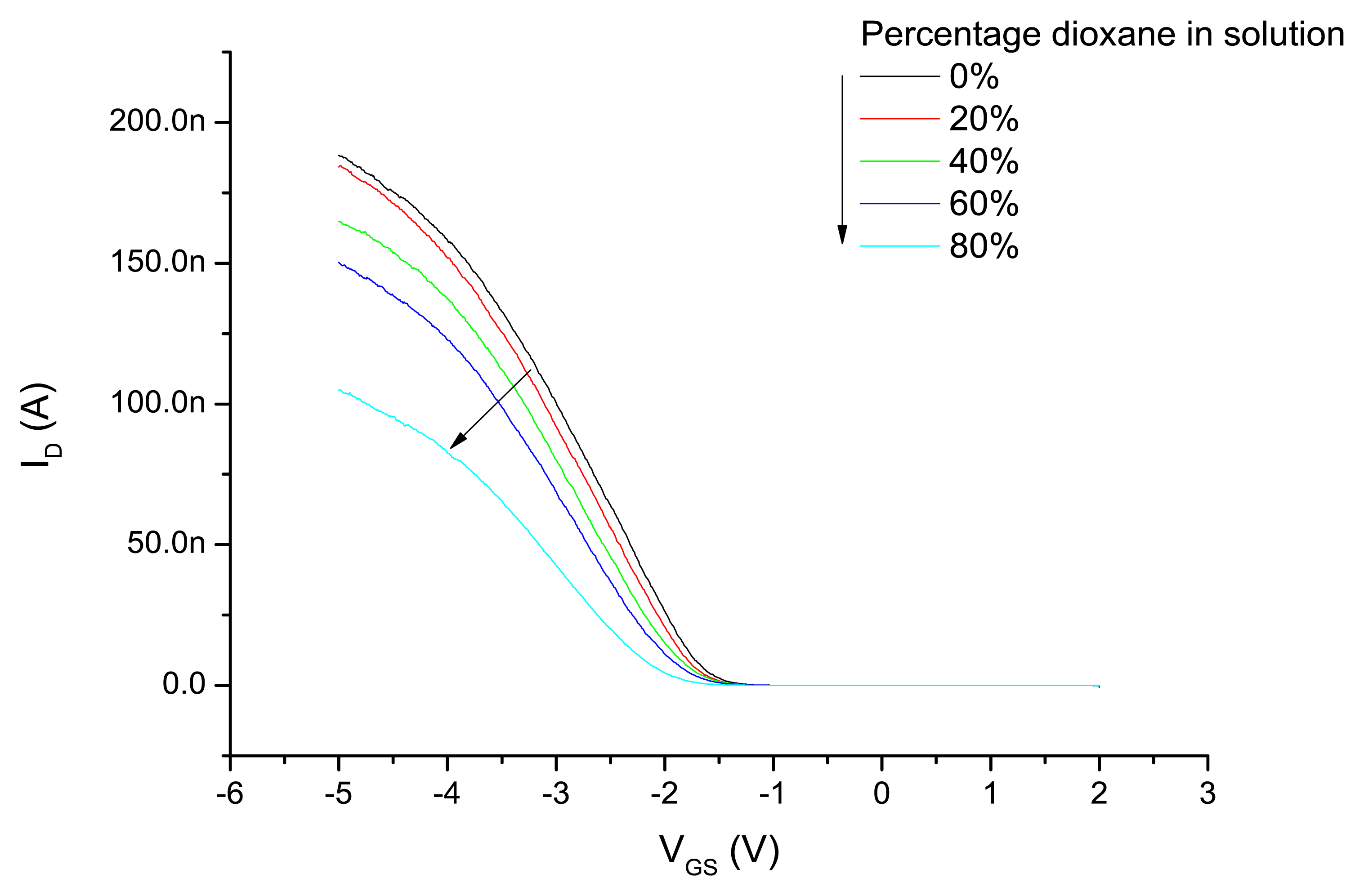
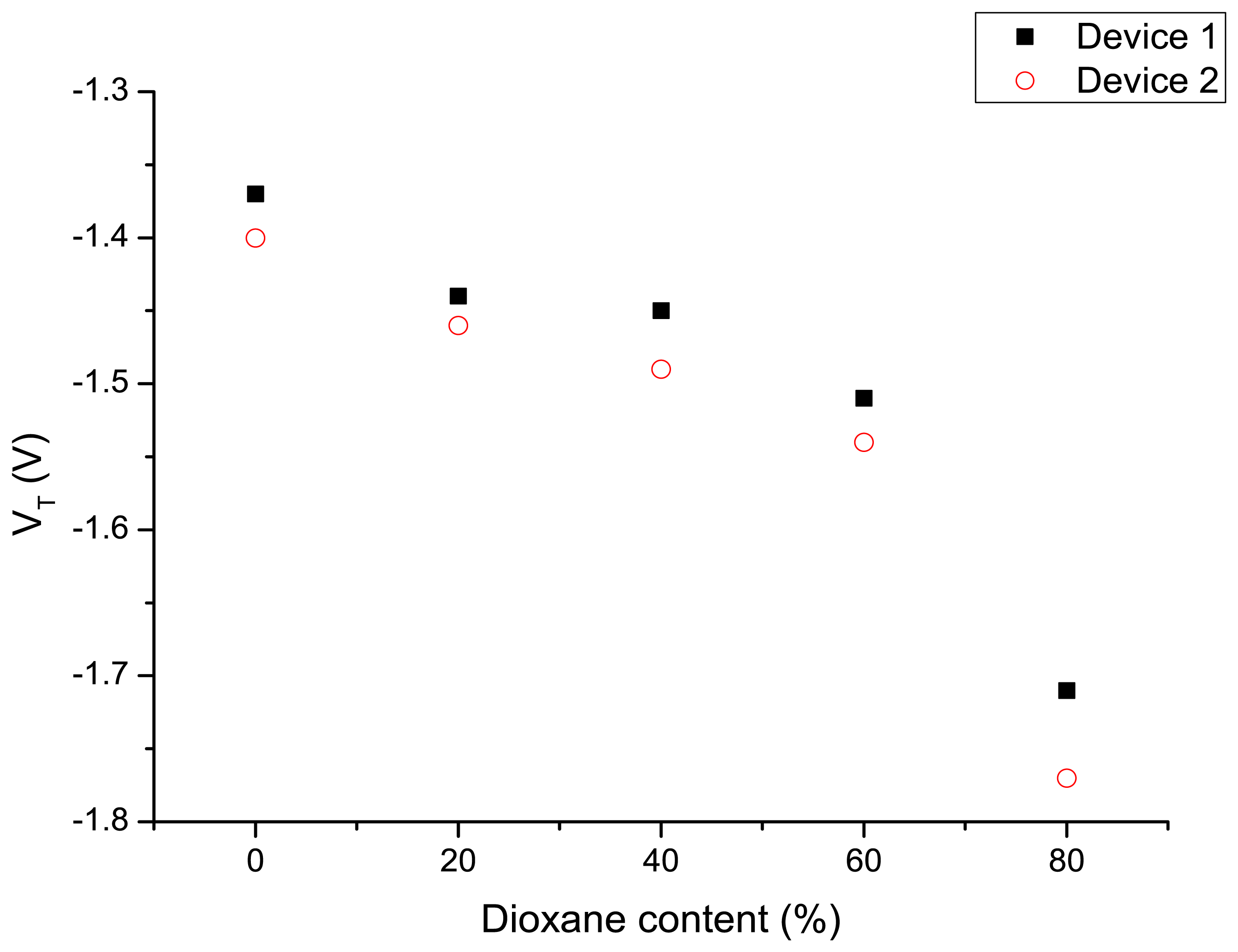
Subsequent to the experiments with the different modes of applying the gate potential, the device was exposed to water–dioxane mixtures and the ID-VGS characteristics are measured as described above by applying a variable potential to the Ag/AgCl electrode and the back gate connected to ground. The results are shown in Figure 4. Increasing dioxane content of the water–dioxane mixture required the application of a more negative gate potential to arrive at the same drain current. From the ID-VGS curves the threshold voltages were determined and plotted as a function of the dioxane content in Figure 5. A more negative VT was observed with increasing dioxane content.
The origin of this observation can be attributed to a decrease of capacitance of the liquid with increasing dioxane content, resulting in an increased negative gate potential to keep the source-drain current constant. However, it is also possible that the reduced dielectric constant of the liquid reduces the dissociation of the surface silanol groups at the oxide interface. This results in a decreased surface charge at a certain proton concentration in the solution. In that case an apparent lower pH value is measured. To compensate for this reduced negative surface potential a more negative potential has to be applied on the gate electrode. To estimate the effect we compare the pKa values of protonated water and protonated dioxane, which are −1.74 and −2.92, respectively [40]. Therefore, protonated dioxane is slightly more acidic than protonated water, and concordially water is a stronger base than dioxane.
It is thus expected that upon increasing the content of dioxane in the water–dioxane mixtures, proton dissociation of the surface silanol groups is reduced. This is in line with an experimental study on the acid dissociation constants of several acids in water–dioxane mixtures [41]. We measured the pH of water–dioxane mixtures using a glass electrode and found that the pH meter reading decreased upon the addition of dioxane. This decrease can also be explained by the decreased dissociation of silanol groups now at the glass electrode surface [42]. In addition, the ionic product of water (pKw) will also decrease upon increasing dioxane fraction [43]. However, that effect reduces the proton concentration, and—if dominant—will increase the surface silanol group dissociation. Since that was not observed in the nanowire experiments, it is concluded that this effect is not dominant. Returning now to our observations on the SiNW-based devices, both the reduced dielectric constant of the water–dioxane medium, i.e., a lower capacitance of that medium, and the reduced dissociation of the surface silanol groups explain the increase VT necessary to restore the nanowire conductance.
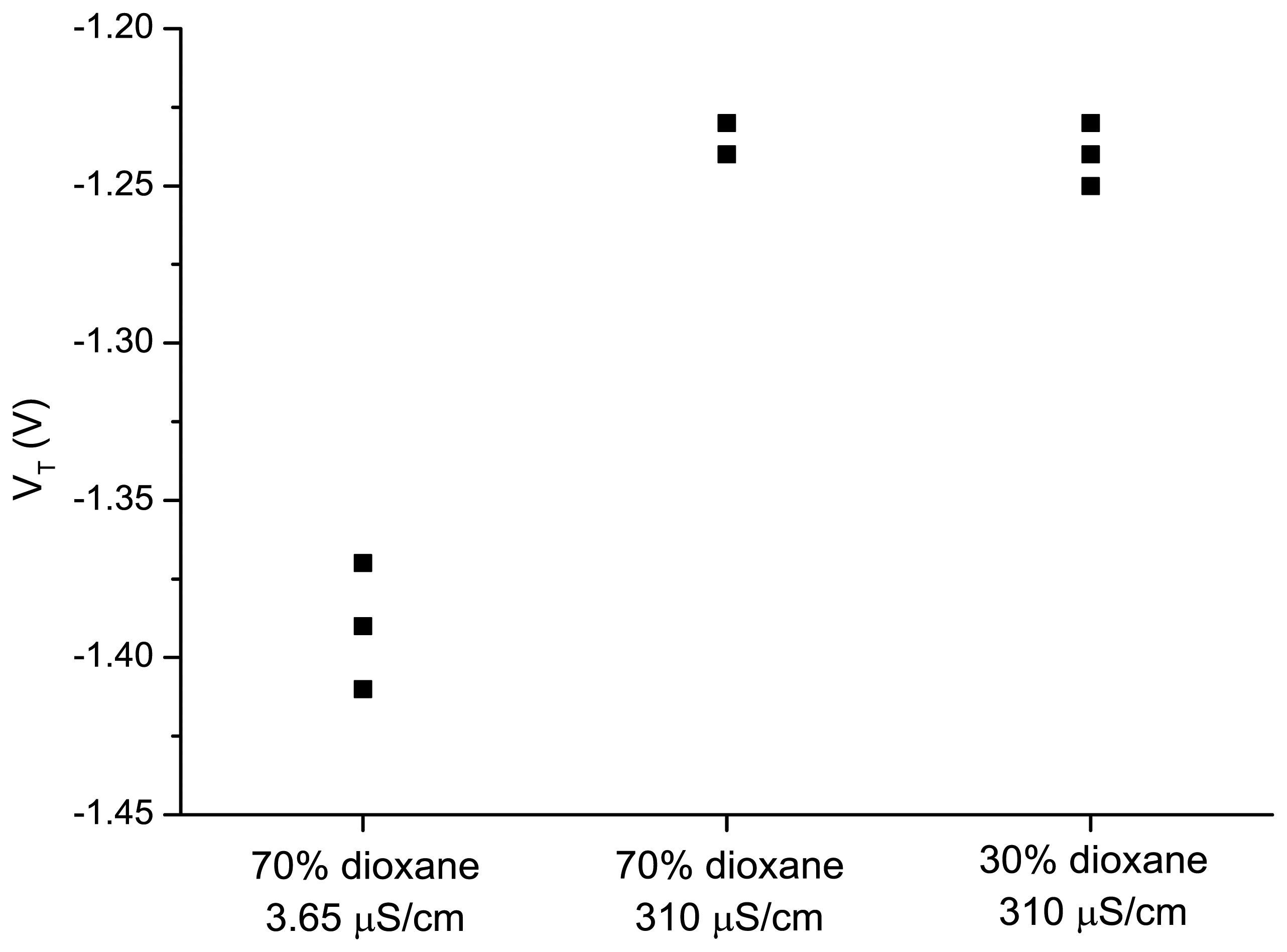
To discriminate between these two possibilities we have investigated the change of the medium capacity, by changing the electrolyte concentration and therefore the electrical conductance. A higher fraction of dioxane decreases the conductance and decreases the capacity. A less negative VT is thus expected for a higher capacity. We have performed the experiments with the following solutions: (a) water/dioxane (30:70 v/v) with a conductivity of 3.65 µS/cm; (b) water/dioxane (30:70 v/v) with tetramethylammonium chloride added to obtain a conductivity of 310 µS/cm; and (c) water/dioxane ratio (70:30 v/v) with tetramethylammonium chloride added to obtain a conductivity of 310 µS/cm. It was observed (Figure 6) that changing the dioxane/water ratio from 30/70 to 70/30 (v/v) at a constant conductivity of 310 µS/cm did not influence the threshold voltage. Reduction of the conductivity to 3.65 µS/cm for a water/dioxane ratio 30/70 (v/v), resulted in a decrease of the threshold voltage. This shows that the conductivity has a larger effect on the gate potential to be applied for maintaining the drain current than changing only the ratio of water to dioxane.
Therefore we come to the conclusion that the effect of water–dioxane ratios on the electrical properties of SiNW are induced by differences in the capacities of the medium between the nanowire and fate electrode as well as by a reduced dissociation of the surface silanol groups.
4. Conclusions and Outlook
In this study, it was demonstrated that there is a different coupling of the gate potential to the SiNW-based device when this potential is applied via the back gate compared to application via a liquid gate. This difference is explained by the BOX layer through which the potential is coupled in the case of the back-gate configuration. This capacitance plays a dominant role over the other relevant capacitances involved. The capacitance of the solution is much less relevant because of its conductivity. Consequently, a reasonable approximation of the system is obtained, even when this layer is not taken into account in the capacitance of the system. Local addition of an individual back gate, which only acts through the area right below the SiNW and which has no capacitive coupling through the liquid, could make a quantitative description of the BG easier. It would also make it possible to individually gate the devices, providing more possibilities for sensor arrays with individual properties.
Furthermore, it was shown that the device characteristics, and most importantly the threshold voltage, are influenced by the solution to which the device is exposed. It is concluded that the change in the threshold voltage as function of dioxane fraction in the medium is determined by a decreased dissociation of the surface silanol groups and a reduced conductivity. Studying the dielectric coupling through the solution will thus only be possible when (1) the surface is passivated with a modification layer which has no interaction with the used solutions and (2) the solutions have a constant conductivity.
When the complete characteristics are taken into account (VT and the slope of the ID-VGS-characteristics, i.e., the transconductance) an even more complete picture of the device characteristics and the influence of certain solvents could be obtained. Combined with assisted computer learning as demonstrated previously by Niskanen et al. [32] a sensor can be constructed from this device. A more detailed approach is needed to explain the observed effects quantitatively, which is beyond the scope of this article. This approach should include a better definition of the capacitance of the solution layer, the charges at the solvent-oxide interface should be taken into account, and adjustments for the absence of a pn-junction need to be added as well as including the presence of mobile charges in the solvent. However, with the simple approach presented in this study it is demonstrated that it is possible to distinguish the different solutions, depending on their conductivity.
To summarize, the results in this article: (1) lead to a better understanding of the electrical response of SiNW-based devices for BG vs. LG modes of operation; and (2) show that working in constant ionic strength is required in aqueous solutions and that corrections for the conductivity of mixed-media solutions are essential.
Acknowledgments
This research was carried out under Project M62.3.09339 in the framework of the Research Program of the Materials innovation institute M2i ( www.m2i.nl). Frank Wiggers is thanked for his experimental work and support. The authors thank the reviewers for highly stimulating comments on a previous version of this manuscript. M.M. would like to thank Ronald Dekker, Ronald van Langevelde and Dick Klaassen for fruitful discussions.
Conflicts of Interest
The authors declare no conflict of interest.
References
- Masood, M.; Chen, S.; Carlen, E.; Berg, A. All-(111) Surface silicon nanowires: Selective functionalization for biosensing applications. ACS Appl. Mater. Interfaces 2010, 2, 3422–3428. [Google Scholar]
- Stern, E.; Klemic, J.F.; Routenberg, D.A.; Wyrembak, P.N.; Turner-Evans, D.B.; Hamilton, A.D.; LaVan, D.A.; Fahmy, T.M.; Reed, M.A. Label-free Immunodetection with CMOS-compatible semiconducting nanowires. Nature 2007, 445, 519–522. [Google Scholar]
- Ramgir, N.S.; Yang, Y.; Zacharias, M. Nanowire-based sensors. Small 2010, 6, 1705–1722. [Google Scholar]
- Zhang, G.-J.; Ning, Y. Silicon nanowire biosensor and its applications in disease diagnostics: A Review. Anal. Chim. Acta 2012, 749, 1–15. [Google Scholar]
- De Smet, L.C.P.M.; Ullien, D.; Mescher, M.; Sudhölter, E.J.R. Organic Surface Modification of Silicon Nanowire-Based Sensor Devices. In Nanowires—Implementations and Applications; Hashim, A., Ed.; InTech: Rijeka, Croatia, 2011; pp. 267–288. [Google Scholar]
- Nair, P.R.; Alam, M.A. Performance limits of nanobiosensors. Appl. Phys. Lett. 2006, 88, 233120. [Google Scholar]
- Nair, P.R.; Alam, M.A. Screening-limited response of nanobiosensors. Nano Lett. 2008, 8, 1281–1285. [Google Scholar]
- Stern, E.; Wagner, R.; Sigworth, F.J.; Breaker, R.; Fahmy, T.M.; Reed, M.A. Importance of the Debye screening length on nanowire field effect transistor sensors. Nano Lett. 2007, 7, 3405–3409. [Google Scholar]
- Sorensen, M.H.; Mortensen, N.A.; Brandbyge, M. Screening model for nanowire surface-charge sensors in liquid. Appl. Phys. Lett. 2007, 91, 102105. [Google Scholar]
- Vacic, A.; Criscione, J.M.; Rajan, N.K.; Stern, E.; Fahmy, T.M.; Reed, M.A. Determination of molecular configuration by Debye length modulation. J. Am. Chem. Soc. 2011, 133, 13886–13889. [Google Scholar]
- Moh, T.S.Y.; Nie, M.; Pandraud, G.; de Smet, L.C.P.M.; Sudhölter, E.J.R.; Huang, Q.A.; Sarro, P.M. Effect of silicon nanowire etching on signal-to-noise ratio of SiNW FETs for (bio) sensor applications. Electron. Lett. 2013, 49, 782–784. [Google Scholar]
- Rajan, N.K.; Routenberg, D.A.; Jin, C.; Reed, M.A. Noise of silicon nanowire BioFETs. IEEE Electron Device Lett. 2010, 31, 615–617. [Google Scholar]
- Mescher, M.; Marcelis, B.; de Smet, L.C.P.M.; Sudhölter, E.J.R.; Klootwijk, J.H. Pulsed method for characterizing aqueous media using nanowire field effect transistors. IEEE Trans. Electron Devices 2011, 58, 1886–1891. [Google Scholar]
- Bashouti, M.Y.; Tung, R.T.; Haick, H. Tuning the electrical properties of Si nanowire field-effect transistors by molecular engineering. Small 2009, 5, 2761–2769. [Google Scholar]
- Bunimovich, Y.L.; Shin, Y.S.; Yeo, W.S.; Amori, M.; Kwong, G.; Heath, J.R. Quantitative real-time measurements of DNA hybridization with alkylated nonoxidized silicon nanowires in electrolyte solution. J. Am. Chem. Soc. 2006, 128, 16323–16331. [Google Scholar]
- Carlen, E.T.; van den Berg, A. Nanowire electrochemical sensors: Can we live without labels? Lab Chip 2007, 7, 19–23. [Google Scholar]
- Tarasov, A.; Wipf, M.; Bedner, K.; Kurz, J.; Fu, W.; Guzenko, V.A.; Knopfmacher, O.; Stoop, R.L.; Calame, M.; Schönenberger, C. True reference nanosensor realized with silicon nanowires. Langmuir 2012, 28, 9899–9905. [Google Scholar]
- Cui, Y.; Wei, Q.; Park, H.; Lieber, C.M. Nanowire nanosensors for highly sensitive and selective detection of biological and chemical species. Science 2001, 293, 1289–1292. [Google Scholar]
- Ingebrandt, S.; Offenhäusser, A. Label-free detection of DNA using field-effect transistors. Phys. Status Solidi A 2006, 203, 3399–3411. [Google Scholar]
- Xuan Thang, V.; Stockmann, R.; Wolfrum, B.; Offenhäusser, A.; Ingebrandt, S. Fabrication and application of a microfluidic-embedded silicon nanowire biosensor chip. Phys. Status Solidi A 2010, 207, 850–857. [Google Scholar]
- Zhang, G.-J.; Agarwal, A.; Buddharaju, K.D.; Singh, N.; Gao, Z. Highly sensitive sensors for alkali metal ions based on complementary-metal-oxide-semiconductor-compatible silicon nanowires. Appl. Phys. Lett. 2007, 90, 233903. [Google Scholar]
- Chen, S.; Bomer, J.G.; Carlen, E.T.; van den Berg, A. Al2O3/silicon NanoISFET with near ideal Nernstian response. Nano Lett. 2011, 11, 2334–2341. [Google Scholar]
- Bergveld, P. Thirty years of ISFETOLOGY What happened in the past 30 years and what may happen in the next 30 years. Sens. Actuators B Chem. 2003, 88, 1–20. [Google Scholar]
- McAlpine, M.C.; Ahmad, H.; Wang, D.; Heath, J.R. Highly ordered nanowire arrays on plastic substrates for Ultrasensitive Flexible Chemical Sensors. Nat. Mater. 2007, 6, 379–384. [Google Scholar]
- Engel, Y.; Elnathan, R.; Pevzner, A.; Davidi, G.; Flaxer, E.; Patolsky, F. Supersensitive detection of explosives by silicon nanowire arrays. Angew. Chem. Int. Ed. 2010, 49, 6830–6835. [Google Scholar]
- Paska, Y.; Stelzner, T.; Christiansen, S.; Haick, H. Enhanced sensing of nonpolar volatile organic compounds by silicon nanowire field effect transistors. ACS Nano 2011, 5, 5620–5626. [Google Scholar]
- Paska, Y.; Haick, H. Interactive effect of hysteresis and surface chemistry on gated silicon nanowire gas sensors. ACS Appl. Mater. Interfaces 2012, 4, 2604–2617. [Google Scholar]
- Paska, Y.; Stelzner, T.; Assad, O.; Tisch, U.; Christiansen, S.; Haick, H. Molecular gating of silicon nanowire field-effect transistors with nonpolar analytes. ACS Nano 2012, 6, 335–345. [Google Scholar]
- Wang, B.; Haick, H. Effect of functional groups on the sensing properties of silicon nanowires toward volatile compounds. ACS Appl. Mater.Interfaces 2013, 5, 2289–2299. [Google Scholar]
- Wang, B.; Haick, H. Effect of chain length on the sensing of volatile organic compounds by means of silicon nanowires. ACS Appl. Mater. Interfaces 2013, 5, 5748–5756. [Google Scholar]
- Ermanok, R.; Assad, O.; Zigelboim, K.; Wang, B.; Haick, H. Discriminative power of chemically sensitive silicon nanowire field effect transistors to volatile organic compounds. ACS Appl. Mater. Interfaces 2013, 5, 11172–11183. [Google Scholar]
- Niskanen, A.O.; Colli, A.; White, R.; Li, H.W.; Spigone, E.; Kivioja, J.M. Silicon nanowire arrays as learning chemical vapour classifiers. Nanotechnology 2011, 22, 295502. [Google Scholar]
- Chen, S.; Zhang, S.-L. Contacting versus insulated gate electrode for Si nanoribbon field-effect Sensors operating in electrolyte. Anal. Chem. 2011, 83, 9546–9551. [Google Scholar]
- Guan, W.; Rajan, N.K.; Duan, X.; Reed, M.A. Quantitative probing of surface charges at dielectric-electrolyte interfaces. Lab Chip 2013, 13, 1431–1436. [Google Scholar]
- Gao, X.P.A.; Zheng, G.F.; Lieber, C.M. Subthreshold regime has the optimal sensitivity for nanowire FET biosensors. Nano Lett. 2010, 10, 547–552. [Google Scholar]
- Mescher, M.; de Smet, L.C.P.M.; Sudhölter, E.J.R.; Klootwijk, J.H. Robust fabrication method for silicon nanowire field effect transistors for sensing applications. J. Nanosci. Nanotechnol. 2013, 13, 5649–5653. [Google Scholar]
- Åkerlöf, G.; Short, O.A. The dielectric constant of dioxane–water mixtures between 0 and 80°. J. Am. Chem. Soc. 1936, 58, 1241–1243. [Google Scholar]
- Zhang, X.G. Electrochemistry of Silicon and Its Oxide; Kluwer Academic Publishers: New York, NY, USA, 2004. [Google Scholar]
- Sze, S. Physics of Semiconductor Devices; John Wiley & Sons: New York, NY, USA, 1986. [Google Scholar]
- Perrin, D.D. Covalent Hydration in Nitrogen Heteroaromatic Compounds: II. Quantitative Aspects. In Advances in Heterocyclic Chemistry; Katritzky, A.R., Ed.; Academic Press: New York, NY, USA, 1965; Volume 4, pp. 43–73. [Google Scholar]
- Lynch, C.C.; La Mer, V.K. Acid dissociation constants in dioxane–water mixtures by potentiometric titration. J. Am. Chem. Soc. 1938, 60, 1252–1259. [Google Scholar]
- Shukla, J.P.; Tandon, S.G. Corrections to pH measurements for titrations on dioxane–water mixtures. Electroanal. Chem. Interfacial Electrochem. 1972, 35, 423–427. [Google Scholar]
- Shukla, J.P.; Subramanian, M.S. Thermodynamics of proton dissociation of acetylacetone and 3-methylacetylacetone in dioxane–water mixtures. Thermochim. Acta 1980, 35, 293–305. [Google Scholar]


© 2014 by the authors; licensee MDPI, Basel, Switzerland. This article is an open access article distributed under the terms and conditions of the Creative Commons Attribution license ( http://creativecommons.org/licenses/by/3.0/).
Share and Cite
Mescher, M.; Brinkman, A.G.M.; Bosma, D.; Klootwijk, J.H.; Sudhölter, E.J.R.; De Smet, L.C.P.M. Influence of Conductivity and Dielectric Constant of Water–Dioxane Mixtures on the Electrical Response of SiNW-Based FETs. Sensors 2014, 14, 2350-2361. https://doi.org/10.3390/s140202350
Mescher M, Brinkman AGM, Bosma D, Klootwijk JH, Sudhölter EJR, De Smet LCPM. Influence of Conductivity and Dielectric Constant of Water–Dioxane Mixtures on the Electrical Response of SiNW-Based FETs. Sensors. 2014; 14(2):2350-2361. https://doi.org/10.3390/s140202350
Chicago/Turabian StyleMescher, Marleen, Aldo G.M. Brinkman, Duco Bosma, Johan H. Klootwijk, Ernst J.R. Sudhölter, and Louis C.P.M. De Smet. 2014. "Influence of Conductivity and Dielectric Constant of Water–Dioxane Mixtures on the Electrical Response of SiNW-Based FETs" Sensors 14, no. 2: 2350-2361. https://doi.org/10.3390/s140202350