Nanoporous Anodic Alumina Platforms: Engineered Surface Chemistry and Structure for Optical Sensing Applications


Abstract
: Electrochemical anodization of pure aluminum enables the growth of highly ordered nanoporous anodic alumina (NAA) structures. This has made NAA one of the most popular nanomaterials with applications including molecular separation, catalysis, photonics, optoelectronics, sensing, drug delivery, and template synthesis. Over the past decades, the ability to engineer the structure and surface chemistry of NAA and its optical properties has led to the establishment of distinctive photonic structures that can be explored for developing low-cost, portable, rapid-response and highly sensitive sensing devices in combination with surface plasmon resonance (SPR) and reflective interference spectroscopy (RIfS) techniques. This review article highlights the recent advances on fabrication, surface modification and structural engineering of NAA and its application and performance as a platform for SPR- and RIfS-based sensing and biosensing devices.1. Introduction
In recent years, an increasing amount of research has been focused on exploring the production of novel nanoporous materials and their application for developing highly sensitive chemical and biosensing devices. These novel analytical devices based on nanoporous materials are cost-effective, highly sensitive due to the large surface-to-volume ratio, and additionally show excellent selectivity when coupled to biorecognition elements [1]. In particular, nanoporous materials synthesized by electrochemical techniques such as porous silicon (pSi), nanoporous anodic alumina (NAA), and titania nanotube arrays (TiNTs) are the top choice of researchers as chemical and biosensing substrates [2,3]. These nanoporous materials have been combined with various optical (e.g., surface plasmon resonance, reflective interference, optical waveguiding, Raman spectroscopy and others) and physical (e.g., electrochemical or impedance technique, piezoelectric, surface acoustic wave and so on) detection methods to develop highly innovative and capable analytical tools [3]. Amid these nanoporous materials, NAA prepared by anodization of aluminum foil, possesses outstanding chemical, optical, and mechanical properties such as chemical resistance, thermal stability, hardness, biocompatibility and large specific surface area. Particularly, its high specific surface area to volume ratio is dearly useful to enhance optical signals when target molecules (analytes) are attached inside the nanopores [3,4]. Therefore, NAA is an excellent platform to develop sophisticated and relevant applications as selective molecular separation, chemical/biological sensing, catalysis, cell adhesion and culture, data storage, energy generation and storage, drug delivery and template synthesis [3–6]. These properties make NAA substrates excellent platform for developing advanced, smart, simple and cost-effective analytical devices. In addition, the ability to engineer its pore size, geometry, and surface chemistry make NAA even a more versatile nanomaterial as these features can be tuned in order to integrate separation and sensing capabilities into all-in-one devices [3]. Recently, the use of NAA for chemical and biosensing applications has gained a very fast pace with potential for future commercialization. The perfectly organized nanoporous structure of NAA, its optical activity and the ability to modify its structure and chemistry have resulted in its vast application as a substrate for surface plasmon resonance and reflective interference-based detection systems [3]. However, no literature review has highlighted and summarized these developments.
Herein, for the first time, we review the major advances and developments of chemical and biosensing systems based on NAA in combination with surface plasmon resonance (SPR) and reflectometric interference spectroscopy (RIfS). First, we present the fundamental aspects of the fabrication and structure of NAA prepared by electrochemical anodization of aluminum. Next, recent advances on the modification of the surface chemistry of NAA using various techniques are reported. Then, we present the most outstanding works in structural engineering of NAA relating aimed at engineering its optical properties. Finally, we present examples of recent advances on SPR and RIfS chemical and biosensing systems based on NAA, providing details of their principles, performance and practical applications.
2. Fabrication and Structure of NAA
Aluminium oxide has been used since the early 1900s due to its chemical and corrosion resistance properties. Keller et al. in 1953, for the first time, described the structure of anodically grown alumina as a close-packed hexagonally organized duplex structure with a porous and a barrier type oxide layer [7]. In general, the structure of self-organized NAA can be described as a matrix of alumina with close-packed arrays of hexagonally-arranged cells with a cylindrical pore at its center that grows perpendicularly to the surface of the aluminum substrate [8]. It is noteworthy that during anodization an electrochemical equilibrium between the rate of oxide growth and its dissolution through the barrier layer at pore bottom is achieved, which is essential for steady state growth and hexagonal packing of nanopores [9,10]. Free-standing NAA substrate can be obtained by selectively etching the underlying aluminum after anodization. Membrane type NAA can be produced by further etching the oxide barrier layer at the pore bottom. This results in membranes with vertically-straight nanochannels. The key structural parameters of NAA are pore diameter (Dp), inter-pore distance (Dint), pore length (Lp) and oxide barrier layer thickness (Lb). Figure 1 presents a schematic of a typical NAA structure along with scanning electron microscopy (SEM) images of its top and cross-sectional surface. The structural features of NAA (i.e., Dp, Dint, Lp, and others) can be precisely controlled by the anodization conditions. In this regard, the geometric features of NAA can be varied in the range of 10–400 nm for pore diameter, 50–600 nm for inter-pore distance, from several nanometers to hundreds of micrometers for pore length, and 30–250 nm for the oxide barrier layer thickness. Other important characteristic parameters of NAA are its pore density (δp) and porosity (P), which can be obtained in a range between 109–1011/cm2 and 5%–50%, respectively [9,11]. During the last decades, the effect of the anodization conditions on the structural features of NAA and self-organizing of pores has been extensively investigated. Anodization parameters such as the anodization voltage, electrolyte type, concentration and temperature have been recognized to be the most critical to control the self-ordering process and the geometry of the resulting NAA structures [11–13]. Aqueous solutions of sulphuric acid (H2SO4), oxalic acid (H2C2O4) and phosphoric acid (H3PO4) are the most commonly used electrolytes for preparation of NAA by conventional anodization process at voltages of 25, 40, and 195 V, respectively [14–16]. This process is called “mild” anodization (MA) as moderate voltages and temperatures are used during the anodization. Other acids have also been reported to yield self-organization of NAA pores, which include aqueous solutions of citric, malic, malonic, tartaric and sulfamic acids [12,17–21]. However, the pore organization achieved with these acid electrolytes is poor in comparison to the conventionally used acids (i.e., sulphuric acid, oxalic acid, and phosphoric acid). Each acid electrolyte has its respective optimum anodization voltage and temperature, which leads the pore growth under self-organizing conditions [22]. Self-organizing conditions for different electrolytes are provided in Table 1
The major milestone in the history of NAA fabrication was reported in 1995, when Masuda and Fukuda successfully prepared highly self-organized NAA with very narrow size distribution and extremely high aspect ratios by using a two-step anodization process [14–16]. In this approach, the porous oxide layer obtained by first anodization is selectively removed to pre-structure the aluminum (Al) surface. This leads to perfect self-organization of pores from top to bottom during the second anodization step. Pre-structuring of Al surface improves the pore arrangement during two/multi-step anodization. However, the slow pore-growth rate in the range of 2–7 μm/h (depending on the electrolytic conditions) is an inherent disadvantage of mild anodization. This problem was solved by a new anodization approach called “hard” anodization (HA) introduced by Gösele and co-workers [8]. Under HA conditions (i.e., high voltages and low temperatures) considerably higher pore-growth rates in the range of 50–100 μm/h could be attained. These two anodization regimes (i.e., MA and HA), under different electrolytic conditions combined with chemical etching, provided new approaches to engineer the structure of NAA with desired pore dimensions and shapes. Several strategies like periodic anodization profiles (voltage or current) with or without replacement of the acid electrolyte have been successfully explored to fabricate NAA with complex pore geometries. These electrochemical approaches have made it possible to fabricate NAA with different pore morphologies, including funnel-type, branched pores, periodically-shaped pore structures, and hierarchical and multi-structured pores. These nanostructures have been demonstrated using the aforementioned anodization and post-synthesis treatment processes [24–28]. This ability to structurally engineer the pores of NAA ad lib in combination with current surface modification methods provides new tools to modify and improve the properties of NAA for developing highly sensitive and selective chemical and biosensing systems. Notice that highly ordered NAA structures can be produced by other nanofabrication approaches, which have been established to precisely control the growth of NAA. Some of them are stamp imprinting and lithography techniques (i.e., colloid sphere lithography, electron-beam lithography, focused-ion beam lithography, holographic lithography, direct laser writing lithography and Ar plasma etching). The choice of the fabrication technique depends on the scale of required pore arrangement, grade and arrangement of organization and pore size and shape. The structural (i.e., pore diameter, pore length and inter-pore distance) and chemical (i.e., distribution and content of impurities, crystallographic phase) properties of NAA are crucial in determining its optical properties. Thus, the fabrication and structural engineering become the key factors when designing optical sensing devices based on NAA.
3. Properties, Surface Chemistry and Surface Functionalization of NAA
3.1. Properties of NAA
NAA is a magnificent platform for developing chemical and biosensing devices due to its distinctive physical and chemical properties. Optical characteristics of NAA such as its photoluminescence (PL), transmittance, reflectivity, and absorbance can be used as principle of detection in highly sensitive and selective chemical and biosensing tools [3]. The pores of NAA can also act as container for holding chemical and biological payloads/molecules that take part in recognition reaction. Another advantage of NAA is that all the microfabrication and miniaturization techniques available for silicon technology can be readily employed for fabricating NAA structures. In this regard, the generation of micropatterns on NAA structures is very useful approach for the development of microfluidics and microarray-based sensing devices. It is worth stressing that the presence of impurities in the inner layer of pores (i.e., close to the pore center) and high density of hydroxyl groups make functionalization of NAA very simple using various techniques (e.g., chemical vapour deposition, sol-gel, dip coating, self-assembly, atomic layer deposition and others). These processes can be used to endow NAA with chemical/physical selectivity toward target molecules (e.g., antigens, DNA, proteins, and enzymes) [29]. These modifications can specifically be aimed at enhancing a wide range of properties of NAA such as its reflectivity, hydrophobicity or hydrophilicity, anti-fouling, and chemical resistance, depending upon its intended application.
3.2. Surface Chemistry and Surface Functionalization of NAA
NAA possess a layered surface chemistry with electrolytic impurities distributed in an onion-like layered manner. It is intended that the chemical structure of NAA is composed of an outer layer close to the center of pore and an inner layer away from the central pore. The outer layer is composed of aluminium oxide (Al2O3) contaminated with acid electrolyte impurities and the inner layer is mainly composed of pure Al2O3 [22]. This has been proven previously by several investigations, however, the number of layers reported by each study is different. Thompson et al. argue that chemical structure of NAA has two layers of onion-like structure where the outer layer is contaminated with anionic species form electrolyte and the inner layer is dense pure alumina [30]. However, there are other studies that point out that the chemical structure of NAA actually consists of more than two layers. As for this, Yamamoto et al. revealed that the chemical structure of NAA is composed of three chemical layers as indicated by its photoluminescence spectrum after specified chemical etching steps [31]. A recent study by our group on the other hand suggests that the real chemical structure of NAA is composed of four onion-like layers with decreasing electrolytic impurities from the outer to the inner layer [32]. A schematic of the chemical structure of NAA is provided in Figure 2.
The chemical dissolution of NAA was monitored in real-time by reflectometric interference spectroscopy and changes in effective optical thickness (OTeff) and intensity of the OTeff peak lead to the aforementioned conclusion. A vast number of surface modification techniques have been developed to protect NAA from acidic environment and impart specific functionalities to its surface. These techniques can be divided into two main categories as physical/gas-phase deposition (i.e., thermal vapor deposition, chemical vapor deposition (CVD), plasma polymerization and atomic layer deposition (ALD)) and chemical modifications (i.e., self-assembly processes of silanes, organic and phosphonic acids, layer-by-layer deposition, polymer grafting, sol–gel processing, electrochemical and electroless deposition) [29]. Subsequent modifications of these surface functionalities of NAA can be used for either to prepare other functional nanomaterials (e.g., nanorods, nanoparticles, nanotubes) or attach biomolecules inside the pores of NAA. The most commonly used approaches for modifying the surface of NAA are described in Figure 3. Further control on the functionalities of NAA surface can be obtained by using a combination of any of these modification techniques on NAA for specific applications.
3.2.1. Gas-Phase Techniques
Gas-phase functionalization techniques including thermal vapor deposition, sputtering, pulsed laser deposition, chemical vapor deposition and plasma polymerization are employed to deposit a wide variety of materials as metals, metal oxides, nitrides, and carbon nanotubes inside NAA [33]. These methods can be used to tune the properties of NAA for specific applications, the most important examples of which are summarized in the following sections.
Metal Coating Using Thermal Vapor, Sputtering and Electron-beam Deposition
Metals films including gold, silver, platinum, palladium, titanium and nickel are generally deposited on NAA using thermal vapor deposition technique. These films are aimed at improving conductivity, reflectivity and chemical stability of NAA substrates [33]. Coatings of metals such as Au, Pd, Pt and Ti are reportedly used to improved catalytic properties of NAA, whereas Ni or Co coatings impart magnetic properties to NAA substrates. Metal coatings also serve as the basis for further chemical modification of NAA to help in binding various chemical and biological species with particular relevance for optical sensing and molecular separation applications [29]. The main disadvantage of these techniques is that the penetration depth is limited and only the top surface of NAA is modified.
Gold coatings on NAA substrates have been used as a base layer for layer-by-layer assembly of α,ω-diorganophosphonate/zirconium(IV), which plays a crucial role in confining LBL multilayers inside the pores and preventing them from being suspended over the top of the NAA substrate [34]. Platinum coatings were used by Toh and coworkers to apply electric field to the NAA membrane for separation of charged proteins. Additionally, the same group achieved size-selective separation by increasing the thickness of the sputtered Pt layer [35,36]. Hexagonal arrangements of NAA pores has been exploited by several groups to prepare surface enhanced Raman scattering (SERS) substrates by depositing noble metals on it [37,38]. Qui et al. deposited an Ag layers on the top surface of NAA templates using a direct-current magnetron sputtering. The resulting metal caps on the surface act as Raman hot spots (Figure 4) [37]. This nanocap SERS-active hot-spot structure provides new opportunities for the fabrication of robust, exceptionally sensitive, cost-effective and large-area chemical and biological sensors. Béron et al. fabricated highly ordered patterned Permalloy nanometric structures by depositing Fe-Pd using ion beam sputtering on top of an anodic aluminium oxide nanoporous template. Their micro-magnetic simulations indicate the presence of Permalloy on one side of the pores, forming an anisotropic nanopillar array combined with an antidot array [39,40].
Plasma Polymer Deposition
Plasma polymerization can be used to deposit reactive and biocompatible polymer films with controlled thickness and chemical functionality with a wide range of functional groups, including amine, carboxyl, hydroxyl, epoxy and aldehyde groups. Brenov et al. for the first time, reported on the modification of NAA by plasma polymerization [41]. They prepared Janus-type NAA membranes by depositing hydrophobic fluorocarbon polymer from plasma polymerization of C4F8 on one side of the NAA membranes while the other side was left unmodified. Water contact angle (WCA) on the hydrophobic side of the NAA membranes was reported (WCA) 150°, while the other side had a WCA lower than 20°. Additionally, the pore diameter on the functionalized side of the NAA membranes was reduced from 160 to 80 nm. In order to improve both structural and surface properties of NAA membranes, Losic et al. functionalized their top surface by plasma polymerization of n-heptylamine. They were able to precisely tune the pore diameter of NAA from 20 nm to <5 nm by adjusting the time duration of the plasma deposition [42]. The process yielded an amine terminal rich surface. However, it is worthwhile noting that this functionalization approach is limited to surface-based applications due to the poor depth penetration inside the nanopores of NAA (Figure 5).
Atomic Layer Deposition (ALD)
ALD enables the precise deposition of a broad range of materials, including oxides, nitrides, sulfides and metals coatings. The resulting coatings present high mechanical, chemical and thermal stability, and optical activity. This technique has been extensively exploited for modifying the inner surface of NAA as a result of its penetration distance inside nanopores. Studies on ALD modification of NAA demonstrate that silica, titania and alumina can be controllably deposited inside NAA pores to reduce its pore dimensions, improving its catalytic, optical and transport properties and generate 1D nanostructures [43–46]. In this regard, Velleman et al. deposited silica (SiO2) inside NAA by ALD method to reduce the pore diameter and subsequent modification with specific silane chemistry, which endowed NAA with chemical selectivity towards transporting dye molecules [5]. In addition, ALD has been used to prepare ultra-high aspect ratio nanotubes/wires of various materials, including pure metals (Cu, Ni, and Co) and their oxides (e.g., ZnO, TiO2, and ZrO2) [46–49]. For example, highly uniform, densely packed and vertically aligned TiO2 nanotubes were fabricated by ALD inside NAA templates using TiCl4 as a precursor. The NAA template was then chemically removed to yield nanotubes with perfectly controllable tube diameter, spacing and wall thickness [50]. In a similar manner, ZnO-nanowires were produced by ALD deposition inside NAA templates [51]. Bachmann and co-workers fabricated magnetic nanotube arrays in NAA templates with modulated pores by means of depositing Fe3O4 via ALD using ferrocene and ozone as precursors (Figure 6) [52,53].
Chemical Vapor Deposition (CVD)
Chemical vapor deposition (CVD) involves dissociation of gaseous molecules by heat, light or plasma to form stable and conformal films on a substrate. CVD is mostly used to grow carbon nanotubes (CNTs) inside NAA pores [54–56]. This process provides vertically aligned arrays of CNTs with controlled dimensions. The carbon layer grows inside the NAA pores via pyrolysis of carbon source (mainly acetylene gas) at elevated high temperature (>600 °C) for varying time [57]. A wide range of carbon sources (either as liquid, gas or solid) have been used for growing CNTs. Recently, our group demonstrated the ability of this technique to recycle plastic waste and convert it into CNTs inside NAA templates (Figure 7) [58]. These CNTs-NAA membranes were demonstrated to be useful for tuning the transporting of dye molecules. In other recent studies by our group, CVD technique was used to deposit monolayers of organosilane (i.e., APTES and MPTES) inside NAA pores [59,60]. To this end, NAA substrates were heated to temperatures in excess of 110 °C with these silanes under vacuum conditions. APTES modification of NAA substrate were used to selectively bind biomolecules, whereas MPTES (mercapto-silane) modified NAA were used to selectively detect gold and mercury ions in aqueous media.
3.2.2. Wet Chemical Techniques of Surface Modification
Attaching other molecules to the surface of NAA is a productive manner to use its high surface area. The inherent presence of anionic impurities in its structure makes the pore surface of NAA prone to attack by oxides to generate surface hydroxyl groups, which act as nucleation centers for its further covalent functionalization. The advantage of wet chemical approaches is that they are usually based on self-assembly phenomenon, which results in full and uniform monolayer surface coating. Unlike physical surface modification, chemical surface modification result in no noticeable change in the structural properties of the NAA substrate [29]. Several groups of compounds such as carboxylic acids, organosilanes and phosphonic acids have been used to impart selective surface chemistry to NAA surface. These compounds are known to form highly uniform monolayers on NAA surfaces.
Self Assembled Monolayers
Self-assembled monolayers (SAMs) are assemblies of organic molecules formed by spontaneous attachment and arrangement of molecules from the liquid phase onto solid surfaces. SAMs of desired molecules can be prepared on NAA in several ways. Pioneering works were focused on self-assembly of alkanethiols on gold-coated NAA surfaces [61]. This process has been extended to SAMs based on organosilanes and phosphonates, which can present a broader range of functional terminals (e.g., amine, carboxyl, epoxy, etc.).
Organosilane Modification of AAO
Organosilanes can be readily formed onto the native or hydroxylated surface of NAA. Organosilanization of NAA has been effectively used to control its wettability and adsorption properties. Wide varieties of organosilanes are commercially available, which can be covalently bound onto the surface of NAA by simply incubating the hydroxylated NAA substrate in silane solution [62]. A schematic of silanization of hydroxylated NAA is provided in Figure 8.
The variety of silanes used for modifying NAA and their applications are listed in Table 2. Tuning the wettability of NAA surface has been demonstrated by selectively forming SAMs of silanes with hydrophobic terminal groups such as alkyl-trichloro-silanes or perfluoroalkyl-silanes [5,63–65]. Ku et al. demonstrated that alkyl-trichlorosilanes with chain length C1–C8 can be used to effectively render the surface of NAA completely hydrophobic, such that even after fully immersing the NAA into an aqueous medium (buffer in this case), pores remain filled with air [65]. In contrast, silanes with active functional groups as PEG-silanes, amine-terminated silanes, epoxy-terminated silanes and others have been used to increase the wettability of NAA. Functionalization of NAA by PEG-silane has been proven to prevent NAA structures from biofouling for long-term use under in vitro or in vivo conditions, improve biocompatibility for immunoisolation, and to reduce the effective pore diameter of NAA for molecular separation applications [66–68].
Furthermore, SAMs based on silanes have been extensively used as an initial active layer to immobilize other (bio)molecules, polymers, nanoparticles, DNA, cells, quantum dots, and lipid bilayers onto the surface of NAA structures [29,69–72]. Different silane chemistries can be used for immobilizing biomolecules such as growth proteins, peptides, lipid bilayers and antibodies. Amid them, amino-propyltryethoxy silane (APTES) is the most commonly used silane for modification of NAA. APTES modification of NAA was shown to suspend lipid bilayers over the pores by first grafting N-hydroxy-succinimidyl carbonate-polyethylene–glycol (NHS-PEG) and subsequently fusing the vesicle onto the PEG layer [73]. Amine groups in APTES have also been revealed to act as surface-confined initiator for grafting of polymer brushes of poly(γ-benzyl-l-glutamate) (PBLG). PBLG polymer brushes can tailor the filtration and separation properties of NAA membranes [74]. Furthermore, APTES-modified NAA can be used to graft poly-N-isopropylacrylamide (PNIPAM) through atom-transfer radical polymerization (ATRP) [75]. Additionally, APTES-modified NAA supports have been used to assemble and fabricate metal nanoparticles or nanotubes by electroless deposition. Wang et al. synthesised Pd nanotubes using APTES-modified NAA templates, which were treated in an aqueous solution of SnCl2 and HCl and subsequently immersed in a solution of PdCl2 and HCl for specific time to generate Pd nanotubes by electroless deposition approach [76].
Sehayek et al. decorated NAA membranes with electrically conductive nanoparticles by passing them through APTES-functionalized NAA pores [78]. Lahav et al. also demonstrated the fabrication of bimetallic nanotubes of Au-Pd by immobilizing a mixture of Au and Pd nanoparticles inside APTES-modified NAA. This leaded to solidification of nanoparticles and formation of multiwall metallic nanotubes upon drying [79].
Our group demonstrated an innovative approach to attach multifunctional silane-based layers in a single NAA template. This multilayered surface modification approach was achieved by a series of anodization and silanization cycles repeated in a sequential fashion. This approach is useful for applications as membrane filtration and separation, as two different surface chemistries can be obtained with distinctly surface properties [77]. We successfully functionalized the surface of NAA with two or three layers of different silanes (pentafluorophenyl-dimethylpropylchloro-silane (PFPTES), APTES and N-triethoxysilylpropyl-(O-polyethyleneoxide)urethane (PEG-silane)), providing a range of surface functionalities and wettabilities as shown in Figure 9 [77,80]. This approach makes it possible to control the thickness of each functional silane layer by controlling the thickness of NAA grown during each anodization and silanization cycle. We further demonstrated the application of this method by selective transport of hydrophobic and hydrophilic dye molecules through membranes with hydrophobic and hydrophilic layers.
Functionalization with Organic and Phosphonic Acids
Allara and Nuzzo, initially reported on the qualitative and quantitative assessments of self-assembly of n-alkanoic acids of varying carbon chains (16–22 carbons) and terminal groups such as methyl, vinyl or propargyl groups [81,82]. Figure 10 defines the basic attachment process of n-alkanoic acids to NAA. Chang and Suen, displayed successful functionalization of NAA surface with n-alkannoic acids (i.e., carboxylic acids) using a solvent-based functionalization method [83]. Cheow et al. used octanoic and octadecanoic acid as well as fluorinated organic acids such as trifluoroacetic acid, perfluoropentanoicacid and 2,3,4,5,6-pentafluorobenzoic acid, to impart hydrophobicity to NAA surfaces. The highest contact angle achieved by these functionalization approaches was 107° for perfluoropentanoic acid-modified NAA [84]. However, the functionalization process was reversible and the resulting functional monolayers were found to be unstable in aqueous environments. Similarly, Karaman et al. also modified the surface of NAA with a variety of short carbon chain (3–4 carbons) fluorinated and non-fluorinated carboxylic acids [85]. Eliasson's group have also shown that other organic molecules such as stearic acid and methyl stearate can form monolayers onto the surface of NAA [86].
Phosphonic acids, on the other hand, do form stable monolayers on NAA surfaces , but there are only few examples of these compounds self-assembling onto NAA [29]. Recently, Debrassi et al. provided a comprehensive study on the stability of a range of monolayer forming compounds, including 1-hexadecylphosphonic acid (PA: phosphonic acid), 1-hexadecylcarboxylic acid (CA: carboxylic acid), 2-hydroxyhexadecylcarboxylic acid (2OHCA: α-hydroxycarboxylic acid), 1-hexadecyne (YNE: alkyne), 1-hexadecene (ENE: alkene), and 1-hexadecyltrimethoxysilane (SIL: silane) [87]. NAA modified with phosphonic acids was the most stable over a pH range 4–8 and temperatures up to 80 °C. They also found that the stability of NAA substrate modified with PA depends strongly on the terminal functional group of the monolayer. For instance, hydrophobic layers were less susceptible to pH and temperature changes than hydrophilic ones. In recent studies by our group, water soluble phosphonic acid (i.e., 2-carboxyethyl phosphonic acid) was used to further attach streptavidin onto the surface of NAA [88,89]. These streptavidin-modified NAA substrates were then employed for impedance-based sensing of biotin (analyte) in aqueous buffer solution.
Lipid Bilayers
Lipid-bilayers are known to mimic cell membranes to a great extent, although their poor stability hinders their applications in several fields. NAA is accepted as a suitable substrate for supporting lipid-bilayers as different assemblies of lipid-bilayers can be obtained depending on the structural features of NAA and deposition methods with the ability to suspend lipid-bilayer on the NAA membrane top or confine them inside the nanopores [90,91]. Suspended lipid-bilayers on NAA substrates have shown long-term stability and act as channels for transporting ions. These suspended lipid-bilayers were fabricated by fusing lipid vesicles on gold-coated NAA substrates pre-treated to form SAMs of alkanethiols with negatively charged head group. Their fabrication approach consisted of gold coating of NAA surface followed by formation of a SAM of alkanethiols with a negatively charged head group [90,92,93]. Similarly, confined lipid-bilayers were fabricated using silanes-coated NAA membranes to achieve fusion of lipid vesicles inside the nanopores [94]. Smirnov and Poluektov, used this technique to deposit multiple lipid-bilayers and obtain lipid nanotubes [95]. They were also able to control the thickness of the lipid wall and confirmed the formation of lipid nanotubes through electron paramagnetic resonance, nuclear magnetic resonance spectroscopy and fluorescence microscopy.
Largueze et al. used a PEG-triggered fusion of lipid vesicles to deposit tethered lipid bilayers inside the pores of NAA [73]. To this end, NAA pores were functionalized with APTES and one side of the NAA membrane with a SAM of undecanethiol after gold coating. Then these multifunctional NAA membranes were incubated with lipid vesicles. After a fixed period of time these lipid vesicles were fused to NAA pore walls using PEG as a trigger (Figure 11). The potential of fabricating lipid-bilayers lies in designing sensitive biomimetic nano-channels that can be used for ion transporting and sensing applications.
Layer-by-Layer Deposition
Layer-by-Layer (LbL) deposition is a very simple, inexpensive, and versatile technique used to obtain thin polyelectrolyte (PE) multilayers, the thickness of which can be controlled with nanometric resolutions, on different substrates. This is achieved by alternatively dipping the substrate into polyelectrolyte solutions of opposite charge (Figure 12a) [96]. This technique was demonstrated to be able to deposit PE layers inside NAA pores. So far, LbL technique has mainly been used to tune the transport properties of NAA membranes, attach nanoparticles or biomolecules inside NAA pores, and fabricate polyelectrolytic nanotubular structures using NAA as a template [29]. In this regard, Balachandra et al. used UV/ozone-treated NAA to adsorb Cu2+ ions, which were used to deposit multi-layers of PAA and PAH inside NAA membranes [97]. Notice that NAA pores remain open (or not blocked) after deposition of up to seven PE bilayers. So far, a vast number of PE combinations and compositions (e.g., PSS/PAH, PSS/PAH, (PSS/PDADMAC)4PSS) have been used to efficiently control the flux, transport, rejection rate and selectivity of solutes through LbL-functionalized NAA membranes [98–100]. Furthermore, Dai et al. used LbL technique to immobilize antibodies inside the nanopores of NAA [101]. In this way, antibodies were immobilized onto the deposited layers of PE composed of [PAA/PAH]3PAH using carbodiimide coupling chemistry (Figure 12b). The same group showed that positively charged PE layers can be utilized to attach citrate-stabilized gold nanoparticles for catalytic applications [102]. LbL technique has employed NAA to synthesize nanotubes of soft materials such as polyelectrolyte polymers, biomolecules, and metal organodiphosphonates. As an example, Li and coworkers introduced the concept of LbL assembly of polyelectrolyte multilayers inside nanoporous alumina template [103,104]. The assembly of polyelectrolyte milt-layers results in polymeric nanotubular structure that display complex but well-controlled wall morphologies and adjustable wall thickness.
They deposited polyallylamine hydrochloride (PAH)/sodium poly(styrene sulfonate) (PSS) from aqueous solutions inside the pores of a NAA membrane assisted by pressure. The alumina walls were subsequently etched using aqueous NaOH solution to obtain liberated flexible (PAH/PSS)3 nanotubes, which replicated the length and outer diameter of the NAA templates used in the synthesis process [103]. Similarly, Martin and co-workers reported the synthesis of DNA nanotubes supported by 1,10-decanediylbis(phosphonic acid) skin using sequential deposition of complementary nucleotides with specific sequences in a NAA membrane [105]. In this process, NAA was first immersed into a solution of (DOP) followed by a solution of ZrOCl2 to form the (DOP)/Zr(IV) supporting skin. The inner surface of the nanotubes resulted from hybridization between multiple double-stranded DNA layers. The same group also demonstrated, for the first time, the synthesis of protein nanotubes by alternately exposing the NAA template to a solution of the glucose oxidase (GOx) or hemoglobin (Hb) [106]. Finally, glutaraldehyde was used as a cross-linker to hold these proteins together. This study also evidenced that GOx nanotubes catalyzed glucose oxidation, whereas heme-electroactivity of Hb nanotubes was retained. Apart from fabrication of novel nanomaterials, LbL has been used to attach functional molecules inside the pores of NAA. For example, Masumoto et al. adsorbed positively charged polyelectrolyte polymer poly-L-lysine inside the pores of NAA to obtain positively charged inner surfaces suitable to bind DNA molecules by electrostatic interactions [107]. A similar strategy has been used to attach noble metal nanoparticles/cubes inside NAA pores (e.g., adsorption of poly(diallyldimethylammonium chloride) to attach gold nanoparticles or PAH/PSS polyelectrolyte multilayers for attachment silver nanocubes) [108].
Sol-Gel Chemistry
Sol-gel assembly process combined with NAA templates has been predominantly used to replicate and prepare novel nanostructures as nanotubes and nanorods or reducing the pore diameter and imparting different surface chemistries to NAA structures (Figure 13) [109]. The most widespread materials for sol-gel synthesis of nanostructures using NAA templates include silica, carbon, metal oxides (e.g., TiO2, TiO2–silica composite, SnO2, NiO, etc.), and polymer-derived SiOC [29]. This technique is based on the hydrolysis of the sol-precursor on the NAA substrate by immersion, dipping or spin coating followed by solvent evaporation and formation of a glassy gel inside the pores [110]. The remaining solvent from the gel-NAA system is removed by subsequent thermal treatment. Sol–gel technique results in synthesis of high purity homogenous and multi-component structures with the ability to further control their properties such as structure, thermal stability and surface reactivity (using precursors with additional functional groups) [111,112]. Lee et al. prepared modified NAA membranes by depositing silica nanotubes using sol-gel template technique [113]. The prepared silica nanotubes were utilized for selective binding and delivery of enantiomeric therapeutic drug. He et al. have demonstrated the fabrication of silica nanotubes with different shapes using funnel-type NAA templates [114–116]. The obtained silica nanotubes with increasing diameter from one end to the other. These nanotubes are called as shape-coded silica nanotubes (SNTs) and were used for specific detection of rabbit anti-IgG from a mixture containing rabbit and human IgG antibodies. They also demonstrated that SNTs can be used for multiple analytes at the same time. As a proof of concept, SNTs featuring three different shape codes were functionalized with rabbit, mouse, and human IgG antibodies, which were subsequently used for simultaneous detection of anti-rabbit and anti-mouse IgG antibodies using a sandwich assay.
Wang et al. prepared carbon-based nanostructures such as carbon fibers and carbon ribbons with a circular mesoporous framework [117]. Phenol-formaldehyde presol was used as a precursor solution along with surfactants such as F127 (EO106PO70EO106) and P123. First, the precursor solution was infiltrated inside the pores of NAA to form gel during the ageing time followed by calcination at 600 °C for 3 h to produce mesoporous carbon nanostructures. The same group prepared mesoporous titania nanotubes within NAA membranes by replacing the carbon source with a titania source (i.e., titanium tetraisopropoxide, TTIP) and employed the mesoporous titania nanotubes as an electrode material in a high rate rechargeable lithium battery [118]. Platschek et al. extended this work by controlling the morphology of synthesized mesoporous carbons by manipulating the sol-to-surfactant ratio and the types of surfactants [119]. Confalonieri et al. displayed deliberate control over the spatial arrangement of nanoparticles using a novel method to assist the self-assembly of magnetic nanoparticles. For this, they spin coated iron oxide nanoparticle (20 nm) on the pretextured Al obtained after removal of first anodized NAA layer. The magnetic nanoparticles were found to form clusters of different arrangements within the valleys of pretextured Al, such as collars, chains and hexagonally closed islands. They used memory effect to probe the strength of magnetic interactions between particles [120].
Electrochemical and Electroless Deposition of Metals
Electrochemical deposition is a simple, inexpensive method for modifying the pores of NAA with metal nanostructures. In comparison to other metal deposition techniques such as CVD, ALD or thermal metal deposition, the electrochemical method does not require expensive equipments and special conditions [121]. Different metal-based nanostructures (i.e., nanowires, nanorods, nanotubes and nanoparticles) have been templated from NAA using this approach [29]. Recent developments in electrochemical deposition have made it possible to deposit multiple metals in the same NAA template for producing alloy nanostructures. Liu et al. prepared segmented Ag-Au alloy nanowires inside NAA templates using electrochemical deposition [122]. Burdick et al. demonstrated the fabrication of multisegmented nanowires of gold with short Ag spacers [123]. Generally, electrochemical deposition is carried out on NAA membranes, which makes it difficult to deposit metal inside thin NAA membranes. To overcome this, Lee et al. developed an alternating current (AC)-based electrochemical deposition technique to assembly gold nanoparticles within NAA membranes [124]. Recent advancement in electropolymerization have lead to fabrication of multisegmented composite nanorods and nanowires of conducting polymers with metals and semiconductors prepared by electrochemical deposition [121]. These metal decorated NAA substrates have been recently used as sensing platforms for such optical techniques as surface enhanced Raman spectroscopy. This was explored by Masuda's Group, who created a 3-D ordered mosaic of gold nanoparticles using the pores of NAA as a mask. The resulting nanostructures were used as sensing platforms in SERS-based detection of pyridine [125]. Electroless deposition, on the other hand, involves reduction of metal cations from an aqueous solution [126]. Martin and co-workers used this method to prepare gold/NAA composites, which were investigated for molecular separation processes [61]. Either metal nanotubes or nanorods/wires can be obtained from electroless deposition depending on the deposition time. So, nanotubes are obtained with short times while solid nanorods/wires can be produced by longer deposition times [121]. Mu et al. fabricated SERS active arrays of Au nanoparticles with tunable particle gaps on NAA substrates. The pH and temperature conditions of the plating bath were reported as the main factor for controlling the size, shape and aggregation of Au nanoparticles during the electroless deposition process [127]. Wang et al. prepared a number of metal nanotubes (i.e., Co, Ni and Cu) using NAA templates via electroless deposition on APTES-modified NAA membranes [76]. The inner diameter and length of the resulting nanotubes were adjusted by controlling the deposition times and the thickness of the NAA template, respectively. Other investigations synthesized Ag nanotubes with lengths over 10 μm inside NAA membranes. Furthermore, Ag nanoparticles of controlled size and smooth surface have been deposited inside NAA using this technique [29].
Lee et al. fabricated multisegmented metallic nanotubes by combining electroless and electrochemical deposition methods (Figure 14). In this approach, Sn (II) was first adsorbed onto the pore walls of NAA membranes from a solution of SnCl2. Subsequently, exposure to Ag (I) led to spontaneous reduction and replacement of Sn (II) via a sensitization process, which was repeated several times. Ag nanoparticles decorated inside NAA membrane pores were isolated from each other, thus did not conduct current. Final electrochemical deposition of Au resulted in formation of Au nanotubes with a bimetallic stacked configuration [128]. Zhang et al. used AC electrodiposition to fabricate nanoporous anodic alumina films embedded with Fe. These films display vivid structural colors and magnetic properties. These properties were found to be dependent on oxidation time of aluminum [129].
4. Structural Engineering and Optical Optimization of NAA
The porous architecture of NAA plays a key role in defining its optical properties. The nanoporous structure of NAA can be designed and engineered to produce a broad range of pore geometries with tailored optical properties. Engineered NAA structures can be designed to interact with light in different manners as to confine, guide, transmit, emit, and reflect it. Developments of different electrochemical anodization approaches have made it possible to design and engineer the structure of NAA to produce a new generation of optical nanostructures. So far, a large variety of NAA pore geometries (i.e., modulated, hierarchical, serrated, three-dimensional, funnel-like, and multilayered) have been engineered by using innovative and unique anodization techniques [130–132]. Figure 15 shows SEM images and schematics of some of the most representative NAA structures generated by different electrochemical approaches. The precise engineering of the nanoporous structure of NAA can result in the generation of optically active structures such as distributed Bragg reflectors, microcavities, rugate filters, omnidirectional mirrors and waveguides [132]. These optical nanostructured devices are formed due to the ability of electrochemical anodization process to produce variations in porosity (i.e., refractive index) of the NAA structure depending upon the type and regime of anodization. The most commonly used method to produce porosity variations is to switch between “Hard” and “Mild” anodization regimes repeatedly, which present different levels of porosity (i.e., MA results in 10% porosity while HA only produces NAA with 3% porosity). Lee et al. used this approach to fabricate NAA with pore diameter modulations along the length of the pores (Figure 15a) [8]. In this method, perfectly ordered NAA was first prepared on an electropolished Al substrate in phosphoric acid electrolyte (H3PO4: 0.4 M, 110 V and 10 °C) after imprinting the pattern from a master stamp. After 15 min of anodization in H3PO4 the electrolyte was replaced with 0.015 M oxalic acid (H2C2O4) and further anodized at 137 V at 0.5 °C for 2 min. NAA with highly uniform periodic modulations of the pore diameter and constant inter-pore distance were obtained by repeating the aforementioned two anodization processes. Notice that the anodization voltages were set such that they yield the same inter-pore distance in MA and HA conditions and prevented NAA pores from pore branching. The pore diameter of NAA during each anodization step was controlled by the anodization voltage and the acid electrolyte, whereas the length was controlled by the anodization time. This report inspired and let to overwhelming a number of studies on different electrochemical approaches to generate pore diameter modulations in NAA structures. As for this, Pitzschel et al. fabricated similar pore diameter modulations in NAA using the same electrolytes under different anodization conditions. In this case, the period of nanoimprint from a master stamp was 235 nm. They performed the first MA step under 72 V in 0.4 M aqueous H3PO4 at 10 °C and the hard step was performed under 93 V in 0.15 M H2C2O4 at 5 °C in a 4:1 water/ethanol mixture. They further used this pore modulated structure to synthesize magnetic nanotubes by depositing Fe3O4 using ferrocene and ozone as precursors [53]. Losic et al. on the other hand, used a cyclic anodization approach, where pore modulations along the length are obtained by applying periodic oscillatory current signals with different profiles, amplitudes, and periods (Figure 15b) [24].
Santos et al. showed the fabrication of hierarchical type NAA where first anodization step is to obtain pre-patterned Al chip with concave cavities [133]. Subsequently, these pre-patterned Al chips are anodized under asymmetric anodization conditions (i.e., changing one or more than one anodization conditions than the first anodization). The resulting NAA structure was observed to have multiple pores within single concave cavities, thus called a hierarchical NAA structure. Serrated-type NAA pores were first fabricated by Zhu et al. They also proposed a new growth model for NAA, which emphasizes on the close relationship between pore generation and oxygen evolution during the formation of such NAA structures [134]. This study was further extended by Li et al. who also on the basis of the results obtained from their experiments and simulation attributed the initiation and formation of serrated-like NAA pores to the evolution of oxygen gas bubbles during the anodization [135]. 3-D type nanoporous structure in NAA was obtained by Losic et al. after combining cyclic anodization and wet chemical etching using phosphoric acid [28]. Likewise, Santos et al. combined discontinuous anodization and wet chemical etching steps with phosphoric acid to obtain a similar 3-D NAA pore structure [136].
Another interesting structure based on NAA is the funnel-like NAA, which can be produced by combining multiple anodization and pore widening steps [24,137,138]. This structure features a stack of NAA layers of decreasing pore diameter from top to bottom, therefore called funnel-like NAA structure (Figure 15c) [23]. The length of each stack is controlled by the time of anodization or the total charge (i.e., integrated current passed through the system), whereas the pore diameter in that stack is established by the pore widening time. Nagaura et al. fabricated low aspect ratio funnel-like NAA and studied their structural changes by manipulating the number of anodization and pore widening cycles [137]. The same authors replicated this low aspect ratio funnel-like structure to create nickel films with nanoconical surface morphology [138]. Yanagishita et al. applied similar approach and replicated the funnel-like structure featuring different pore shapes to a polymer by photo-imprinting process [139]. The polymer replicates were studied for their antireflection behavior by measuring the amount of transmitted light. NAA nanostructures with more gradual changes in slope were found to be less reflective. Santos et al. fabricated high aspect ratio funnel-like NAA by controlling the length of each stack very precisely according to the total charge passed through the system. They demonstrated NAA funnel-like structure with two, three, and four stacks [24]. Li et al. reported tailoring of the shape of funnel-like NAA pore structures by new electrochemical approach [140]. They successfully demonstrated the fabrication of linear cones, whorl-embedded cones, funnels, pencils, parabolas and trumpets-like nanopore structures by controlling the fabrication parameters as anodization time, etching time and cycle times. Very recently, we reported on the fabrication of inverted funnel-like NAA, which has increasing pore diameter along the pore length from top to bottom [32]. This innovative structure was achieved by taking advantage of the fact that the chemical dissolution rate of NAA decreases after annealing at temperatures in excess of 100 °C. We made inverted funnel-like NAA with two and three stacks by combining annealing steps and anodization steps. In addition, formation of these inverted funnel-like structures was monitored in real-time using reflective interference spectroscopy method.Multilayered NAA structures can be used to fabricate a broad range of optical nanostructures such as DBRs, optical microcavities, rugate filters and other optical and photonic structures. They consist of multiple layers of NAA segments with different levels of porosity. Multilayered NAA structures have been fabricated by periodically alternating the voltage during the anodization process. Anodization profiles such as stepwise, sinusoidal, pseudo-sinusoidal, saw-like, etc. have been applied to engineer the porosity (i.e., refractive index) of NAA in depth. This allows for specifically designing and engineering the light-matter interaction in NAA for subsequent applications in chemical and bio-sensing. Lee et al., for the first time, displayed the ability to fabricate multilayered NAA via an electrochemical approach consisting of periodic pulses of low and high potential (i.e., voltage in MA and HA regime) [26]. In this study, they performed anodization of pre-patterned Al chips through pulse anodization under potentiostatic conditions in sulphuric and oxalic acids. Nanotubular array structures with periodic neck-like constrictions along the length of the tubes were observed for sulphuric acid electrolyte while NAA with periodically varying pore diameter were observed for oxalic acid electrolyte.
Sulka et al. applied a similar approach to fabricate layered NAA structures, which were subsequently used as templates for fabricating modulated metal nanowires. In another study, they demonstrated the application of this multilayered NAA structure as distributed Bragg reflector (DBR) [141]. The resulting NAA-based DBR structure had periodically modulated layers of NAA with low and high porosity (i.e., refractive index). These DBR mirrors were observed to effectively reflect light in two different ranges of wavelength, which was in good agreement with the mathematical calculated reflection spectrum.
Zheng et al. prepared NAA based DBRs by anodizing Al chips under pseudo-sinusoidal voltage profile in oxalic acid electrolyte [142]. They studied the effect of the anodization temperature on the transmission peak of the prepared DBRs. The results predicted that almost the whole range of visible spectrum can be covered by adjusting the anodization temperature between 7 and 14 °C. Recently, Rahman et al. used an innovative cyclic anodization approach produce NAA-based DBRs [143]. They also studied the effect of pore widening time on the position of the photonic stop-band of the resulting DBRs. This study demonstrated the ability to control the photonic stop-band of these optical nanostructures by modulating the refractive index contrast between the layers through pore widening. More recently, Kumeria et al. fabricated nanoporous rugate filters by anodizing Al chips under pseudo-sinusoidal potentiostatic conditions in oxalic acid electrolyte [132]. They prepared four different types of rugate filters based on NAA and selected the most optimum structure based on their experimental and theoretical modeling (i.e., the Looyenga−Landau−Lifshitz model) for sensing applications. This study demonstrated that optimize optical signals enable the precise control of the optical properties of nanoporous structures for chemical and bio-sensing applications.
5. Optical Sensing Applications
5.1. Plasmon Resonance Sensors Based on NAA
Since the first publication in the late 1970s, the potential of surface plasmon resonance (SPR) for characterization of thin films and monitoring analyte-receptor binding processes at metal interfaces has been greatly recognized [144]. Capabilities of SPR are real-time and in-situ measurements of a wide range of surface interactions, ligand-binding affinity, association/ dissociation kinetics, affinity constants, and highly sensitive surface-concentration measurements. During the last decades, SPR has been exploited such that more than 75% of research on optical biosensing was based on SPR [144]. This extensive exploitation of this sensing technique has resulted in the generation of new SPR configurations (i.e., Grating, Otto, and Kretschmann configurations) and substrates (i.e., nanostructured films, porous materials, nanoparticles, etc.). The use of nanomaterials has led to the discovery of a new type of SPR such as waveguiding and localized SPR (LSPR or LPR) that exclusively occurs in noble metal nanoparticles/structures. Notably, when the noble metal particles/structures (i.e., gold, silver, etc.) are scaled down to nanometric level (i.e., <100 nm), light interacts with particles much smaller than the incident wavelength [144]. This leads to the generation of plasmonic oscillations of a particular frequency that are localized around the nanoparticles. LPR oscillations are dependent on the size, shape and surrounding environment of the nanoparticles/structures. The LPR is sensitive to changes in the local refractive index environment, which can be measured through shifts in the resonance wavelength or resolving the LPR. Recent studies have proven that close organization of metal nanoparticles/structures even leads to enhancement of LPR signals. In recent years, NAA has become a very attractive nanomaterial as a substrate for SPR-based sensing devices in SPR, waveguiding (WG), as well as LPR mode [145–147]. In this regard, typically a thin layer of NAA is either directly grown onto a prism or pre-formed NAA is glued to a metal coated prism using a refractive index matching glue. Surface plasmons are excited by an evanescent electromagnetic wave produced by the incidence of light on the surface under a Kretschmann configuration. In addition, NAA coated with noble metals presents highly organized metallic nano-caps, which have been utilized to excite plasmons under LPR mode and applied for chemical and bio-sensing applications. NAA-LPR-based SPR sensors are simple, inexpensive, compact and portable as it does not require a prism-based setup. Notice that the plasmonic characteristics of the SPR devices depend mainly on the surrounding refractive index within a range of few hundreds of nanometers beyond the metal film in Kretschmann configurations and LPR mode [144]. Thus, a thin layer of NAA within this thickness range can be applied onto the prism and used to develop nanoporous SPR sensors. Lau et al. combined NAA with waveguiding to develop a WG optical sensing platform, which was used to monitor reversible adsorption and desorption of bovine serum albumin (BSA) at different values of pH [146]. Their NAA-WG setup was based on a Kretschmann configuration with an intermediate Au layer between the prism and the NAA platform. A simpler and sensitive setup was developed by Yamaguchi et al. by directly depositing Al onto a prism and anodizing it to generate a nanoporous layer of 200 nm thick. The remaining unanodized Al (17 nm) acted as the metal layer to excite the plasmon for waveguide coupling [148]. Koutsioubas et al. on the other hand, fabricated NAA-based SPR sensors used to detect the formation of SAMs of octadecyl-phosphonic acid (ODP) [145]. Dhathathreyan demonstrated that the similar system can be used to quantify enzyme kinetics reaction [149]. In this study, the enzyme invertase was immobilized in the pores of 3 μm thick NAA layer with a pore diameter of 60 nm. The enzyme-substrate was flowed through a custom made flow cell and the digested product was detected by SPR. This system made it possible to study the activity of the immobilized enzyme, which was determined for different concentrations of sucrose at pH ranging from 3 to 6.5. The SPR results revealed a biphasic kinetics for both the adsorption of the enzyme and its interaction with the substrate. Maximum enzyme activity was observed at pH 4.5. In another study, Lau et al. monitored the grafting of poly(g-benzyl-L-glutamate) (PBLG) within the nanopores of NAA in real-teal time and in-situ using a SPR-NAA system [74]. Their results reveal that the conformation of PBLG inside the nanopores of NAA is due to confinement of polymer chains inside the pores, which was confirmed by comparing the results obtained with NAA and planar silicon dioxide surface. More recently, Hotta et al. used NAA-WG configuration demonstrated by Yamaguchi et al. and studied the enhancement of sensitivity (Figure 16a) [150].
For this, the structure of NAA (i.e., waveguiding layer) on Al (i.e., cladding layer) was carefully engineered in terms of porosity, pore density, thickness, and refractive index to tune and optimize the optical WG and enhance the sensitivity of the system. The performance of the optimized NAA-WG was assessed by monitoring the adsorption of BSA molecules onto the nanopores of NAA. The most optimum NAA-WG sensor resulted in an extraordinarily large red shift (>300 nm) of a waveguide mode on adsorption of BSA. This extraordinary red shift was attributed to the large surface area of NAA, which results in a huge adsorption capacity. The theoretical calculations using Fresnel's equation suggested that the sensitivity of the NAA-WG sensor was much higher than that of conventional SPR sensors.
Another study by the same group, reports on enhancement of fluorescence signal on adsorption of fluorophore-labeled BSA (i.e., BSA-AF) inside the nanopore surface of a NAA waveguiding film [152]. They monitored the adsorption of BSA-AF simultaneously using SPR and fluorescence spectroscopy. Enhancement of FL signal on NAA-WG is attributed to a combination of large surface area of NAA and enhanced field due to waveguiding modes within the pores of NAA. As described above, LPR is another type of widely used SPR mode in combination with NAA substrate coated with noble metals (mostly gold or silver). This results in the formation of highly ordered arrays of metallic NPs of gold or silver (i.e., nanocaps) on the top surface of the NAA. Figure 16b shows a typical LPR-NAA label-free biosensor fabricated on a gold-capped AAO substrate for detection of antigen-antibody binding. So far, NAA-based LPR sensors have been demonstrated for specific detection of proteins (e.g., BSA, avidin, DNA and thrombin) or binding events between biotin-avidin, complementary oligonucleotides, and 5-fluorouracil-anti-5- fluorouracil. In this regard, Kim et al. developed a new optical biosensor based on a gold-deposited NAA chip [151]. They observed that gold nanocaps resulted in an optical LPR pattern that was highly sensitive to the changes in the effective refractive index of the biomolecular layer attaching them. They demonstrated the detection of up to picomolar quantities of un-labeled oligonucleotides and the hybridization with synthetic DNA samples. Hiep et al. deposited gold on the top surface of NAA to form nanocaps and developed a NAA-LPR sensor to detect specific interactions between biomolecules such as biotin and avidin and 5-fluorouracil and anti-5-fluorouracil [147]. Another studies from the same group utilized NAA as a support for plasmonic gold nanoparticles (AuNPs). NAA fabricated by the two-step anodization process was exposed to cationic poly(allyl amine) to attach AuNPs on its surface. The pores of NAA trapped Au nanoparticles. Their experimental and simulation results show that the plasmonic spectra of this NAA-AuNPs composite were enhanced by the interference spectra of the NAA layer. This assembly of AuNPs on NAA substrate showed a high sensitivity towards solutions with different refractive indices [153]. In another study, Hiep et al. combined NAA-LPR with an electrochemical system for sensitive detection of toxic peptide (i.e., melittin, the venom from the honey bees) with a lower limit of detection (LOD) at 10 ng/mL [154]. Yeom et al. used a similar strategy to form gold nanocaps on the top surface of NAA to develop an immunosensor featuring anti-CRP (C-reactive protein, a cardiac and inflammatory biomarker) antibody immobilised on the gold nanocaps [155]. Their system displayed an extraordinary lower limit of detection for CRP antigen at concentration 1 fg/mL due to LPR enhancement of the optical signals from NAA. Kim et al. used a similar system to detect picomolar quantities of untagged oligonucleotides on NAA-LPR platform.
5.2. Reflectometric Interference Spectroscopy (RIfS) Sensors Based on NAA
Reflectometric interference spectroscopy (RIfS) is another highly sensitive optical detection method that is based on the interaction of white light with films at micrometer scale. In this technique, white light is shined on a thin film and reflected at the two interfaces of the thin film resulting in amplification of the reflected light signal at wavelengths corresponding to the optical modes of the Fabry–Pérot (FP) cavity formed by the system thin film–surrounding medium (i.e., the Fabry–Pérot effect) [156]. A model NAA-based reflective interference along with RIfS spectrum and real-time effective optical thickness change curve is presented in Figure 17a. The wavelength of each interference maximum in the RIfS spectrum is governed by the Fabry–Pérot relationship (Equation (1)) [157]:
Interestingly, NAA-RIfS platforms not only can be used to monitor filling of NAA pores and the attachment of analyte molecules to the surface functional groups but also to study the release of molecules such as drugs from NAA substrates. Using this approach, Kumeria et al. monitored the release of a model drug, indomethacin, in real-time under dynamic flow conditions (Figure 17b) [169]. Their results revealed that the process is diffusion-controlled and the rate of drug release depends highly on the flow rate (i.e., the faster the flow rate the higher the drug release from the nanoporous platform). This approach provides more accurate information than conventional in vitro drug release techniques performed under static conditions. A comparative study measuring the sensing performance of RIfS and photoluminescence spectroscopy (PLS) using NAA as substrate was recently reported by Santos et al. (Figure 17c) [60]. First, NAA with most optimum optical signal was obtained depending on the ratio of height to width of the effective optical thickness peak for both PLS and RIfS. This most optimal NAA structure was subjected to detection of glucose and L-cysteine under non-specific and specific binding conditions, respectively. Their results suggested that the type of the analyte molecules and their binding conditions play a crucial role in the determining the sensing performance of a device. Nevertheless, NAA-PLS platforms displayed better sensing performance (i.e., linearity, higher sensitivity toward analytes and lower limit of detection) for both the analytes and binding conditions than NAA-RIfS platforms. Macias et al. fabricated a bilayered funnel-like NAA-RIfS sensing platform [170]. This structurally engineered NAA substrate generates a complex reflectivity spectrum. Their results show that a significant enhancement of the RIfS peak intensity on coating the top surface of the bilayer-NAA with gold layer. This biosensing platform was assessed by detecting BSA molecules and the results demonstrate the ability of bilayer-NAA-RIfS platform to detect BSA only in the effective optical thickness peak corresponding to the top layer and the total layer (i.e., the whole bilayer) based on size exclusion.
6. Future Perspective and Conclusions
We believe that there is still a huge potential for further improvement of basic properties of NAA, which can be utilized for broad and multidisciplinary research fields as materials science, nanotechnology, optics, electrochemistry, cell biology and medicine. Over the last few decades, the different approaches have made it possible to design the structure of NAA, resulting in better control over pore diameter, length, porosity and organization of pores. However, the real understanding of the self-organizing anodization process on aluminum is not complete. Thus, to generate and extend the range of NAA structures available, it is necessary to investigate this phenomenon intensely. For its wider commercial application, the cost is a critical factor for NAA to be used as a consumable, however, the cost of high purity aluminum may be bottom line in this scenario. In terms of surface chemistry, the surface properties of NAA can be finely tuned in limited ways due to inherent properties of the process used to functionalize NAA (i.e., limited coverage, stability, and terminal groups). In the future we may expect more versatile surface functionalization process to achieve chemistries unimaginable with present techniques and several research groups are already working towards it.
This review has summarized and presented the recent progresses in surface functionalization and modification of NAA and the developments for its use in localized plasmon and reflective interference based sensing systems. We have presented a detailed description about structure and surface modifications of NAA. We have also provided detail of the fundamental aspects of LPR and RIfS in combination with NAA platforms along with the most relevant concepts and examples of devices reported based on NAA and these optical techniques. Due to the advanced properties of NAA, it has emerged as a highly attractive alternative for development of broad range stable and functional sensing devices for clinical, industrial and environmental analyses. The ability to modify the surface of NAA with a wide range of functionalities to endow it with desired selectivity and specificity towards target analytes has pushed NAA for applications in several fields. We believe that future developments in structural engineering and chemical modifications of NAA will yield more innovative NAA-based sensing systems. Furthermore, a number of methods to structurally engineer the NAA make it further attractive nanostructures for development of future optical sensing devices. However, this review has demonstrated that there is still plenty of advances and developments to be made in the field of structural engineering, surface modification, and NAA-LPR and NAA-RIfS based sensing platforms.
Acknowledgments
This research was supported by the Australian Research Council (ARC) through the grant No. DE14010054 and the School of Chemical Engineering, The University of Adelaide.
Author Contributions
T.K., A.S. and D.L. contributed equally to this work.
Conflicts of Interest
The authors declare no conflict of interest.
References
- Gyurcsányi, R.E. Chemically-modified nanopores for sensing. TrAC Trends Anal. Chem. 2008, 27, 627–639. [Google Scholar]
- Ghicov, A.; Schmuki, P. Self-ordering electrochemistry: A review on growth and functionality of TiO2 nanotubes and other self-aligned MOx structures. Chem. Commun. 2009, 2791–2808. [Google Scholar] [CrossRef]
- Santos, A.; Kumeria, T.; Losic, D. Nanoporous anodic aluminum oxide for chemical sensing and biosensors. TrAC Trends Anal. Chem. 2013, 44, 25–38. [Google Scholar]
- Ingham, C.J.; ter Maat, J.; de Vos, W.M. Where bio meets nano: The many uses for nanoporous aluminum oxide in biotechnology. Biotechnol. Adv. 2012, 30, 1089–1099. [Google Scholar]
- Velleman, L.; Triani, G.; Evans, P.J.; Shapter, J.G.; Losic, D. Structural and chemical modification of porous alumina membranes. Microporous Mesoporous Mater. 2009, 126, 87–94. [Google Scholar]
- Losic, D.; Simovic, S. Self-ordered nanopore and nanotube platforms for drug delivery applications. Exp. Opin. Drug Deliv. 2009, 6, 1363–1381. [Google Scholar]
- Keller, F.; Hunter, M.; Robinson, D. Structural features of oxide coatings on aluminum. J. Electrochem. Soc. 1953, 100, 411–419. [Google Scholar]
- Lee, W.; Ji, R.; Gösele, U.; Nielsch, K. Fast fabrication of long-range ordered porous alumina membranes by hard anodization. Nat. Mater. 2006, 5, 741–747. [Google Scholar]
- Alkire, R.C.; Gogotsi, Y.; Simon, P.; Eftekhari, A. Nanostructured Materials in Electrochemistry; John Wiley & Sons: Hoboken, NJ, USA, 2008. [Google Scholar]
- Jessensky, O.; Müller, F.; Gösele, U. Self-organized formation of hexagonal pore arrays in anodic alumina. Appl. Phys. Lett. 1998, 72, 1173–1175. [Google Scholar]
- Li, A.P.; Müller, F.; Bimer, A.; Nielsch, K.; Gösele, U. Hexagonal pore arrays with a 50–420 nm interpore distance formed by self-organization in anodic alumina. J. Appl. Phys. 1998, 84, 6023–6026. [Google Scholar]
- Ono, S.; Saito, M.; Asoh, H. Self-ordering of anodic porous alumina formed in organic acid electrolytes. Electrochim. Acta 2005, 51, 827–833. [Google Scholar]
- Losic, D.; Velleman, L.; Kant, K.; Kumeria, T.; Gulati, K.; Shapter, J.G.; Beattie, D.A.; Simovic, S. Self-ordering electrochemistry: A simple approach for engineering nanopore and nanotube arrays for emerging applications. Aust. J. Chem. 2011, 64, 294–301. [Google Scholar]
- Masuda, H.; Fukuda, K. Ordered metal nanohole arrays made by a two-step replication of honeycomb structures of anodic alumina. Science 1995, 268, 1466–1468. [Google Scholar]
- Masuda, H.; Hasegwa, F.; Ono, S. Self-ordering of cell arrangement of anodic porous alumina formed in sulfuric acid solution. J. Electrochem. Soc. 1997, 144, L127–L130. [Google Scholar]
- Masuda, H.; Yada, K.; Osaka, A. Self-ordering of cell configuration of anodic porous alumina with large-size pores in phosphoric acid solution. Jpn. J. Appl. Phys. 1998, 37, L1340. [Google Scholar]
- Surganov, V.; Morgen, P.; Nielsen, J.; Gorokh, G.; Mozalev, A. Study of the initial stage of aluminium anodization in malonic acid solution. Electrochim. Acta 1987, 32, 1125–1127. [Google Scholar]
- Surganov, V.; Gorokh, G. Anodic oxide cellular structure formation on aluminum films in tartaric acid electrolyte. Mater. Lett. 1993, 17, 121–124. [Google Scholar]
- Chu, S.; Wada, K.; Inoue, S.; Isogai, M.; Katsuta, Y.; Yasumori, A. Large-scale fabrication of ordered nanoporous alumina films with arbitrary pore intervals by critical-potential anodization. J. Electrochem. Soc. 2006, 153, B384–B391. [Google Scholar]
- Ono, S.; Saito, M.; Ishiguro, M.; Asoh, H. Controlling factor of self-ordering of anodic porous alumina. J. Electrochem. Soc. 2004, 151, B473–B478. [Google Scholar]
- Mozalev, A.; Mozaleva, I.; Sakairi, M.; Takahashi, H. Anodic film growth on al layers and ta–al metal bilayers in citric acid electrolytes. Electrochim. Acta 2005, 50, 5065–5075. [Google Scholar]
- Nielsch, K.; Choi, J.; Schwirn, K.; Wehrspohn, R.B.; Gösele, U. Self-ordering regimes of porous alumina: The 10% porosity rule. Nano Lett. 2002, 2, 677–680. [Google Scholar]
- Schwirn, K.; Lee, W.; Hillebrand, R.; Steinhart, M.; Nielsch, K.; Gösele, U. Self-ordered anodic aluminum oxide formed by H2SO4 hard anodization. ACS Nano 2008, 2, 302–310. [Google Scholar]
- Santos, A.; Formentín, P.; Pallarès, J.; Ferré-Borrull, J.; Marsal, L.F. Structural engineering of nanoporous anodic alumina funnels with high aspect ratio. J. Electroanal. Chem. 2011, 655, 73–78. [Google Scholar]
- Losic, D.; Lillo, M. Porous alumina with shaped pore geometries and complex pore architectures fabricated by cyclic anodization. Small 2009, 5, 1392–1397. [Google Scholar]
- Lee, W.; Schwirn, K.; Steinhart, M.; Pippel, E.; Scholz, R.; Gösele, U. Structural engineering of nanoporous anodic aluminium oxide by pulse anodization of aluminium. Nat. Nanotechnol. 2008, 3, 234–239. [Google Scholar]
- Meng, G.; Jung, Y.J.; Cao, A.; Vajtai, R.; Ajayan, P.M. Controlled fabrication of hierarchically branched nanopores, nanotubes, and nanowires. Proc. Natl. Acad. Sci. USA 2005, 102, 7074–7078. [Google Scholar]
- Losic, D. Preparation of porous anodic alumina with periodically perforated pores. Langmuir 2009, 25, 5426–5431. [Google Scholar]
- Md Jani, A.M.; Losic, D.; Voelcker, N.H. Nanoporous anodic aluminium oxide: Advances in surface engineering and emerging applications. Prog. Mater. Sci. 2013, 58, 636–704. [Google Scholar]
- Thompson, G.E.; Wood, G.C. Anodic films on aluminium. In Treatise on Materials Science and Technology; Scully, J.C., Ed.; Academic Press. Inc.: New York, NY, USA, 1983; Volume 23, pp. 205–329. [Google Scholar]
- Yamamoto, Y.; Baba, N.; Tajima, S. Coloured materials and photoluminescence centres in anodic film on aluminium. Nat. Lett. 1981, 289, 572–574. [Google Scholar]
- Santos, A.; Kumeria, T.; Wang, Y.; Losic, D. In situ monitored engineering of inverted nanoporous anodic alumina funnels: On the precise generation of 3d optical nanostructures. Nanoscale 2014. [Google Scholar] [CrossRef]
- Lei, Y.; Cai, W.; Wilde, G. Highly ordered nanostructures with tunable size, shape and properties: A new way to surface nano-patterning using ultra-thin alumina masks. Prog. Mater. Sci. 2007, 52, 465–539. [Google Scholar]
- Hou, S.; Harrell, C.C.; Trofin, L.; Kohli, P.; Martin, C.R. Layer-by-layer nanotube template synthesis. J. Am. Chem. Soc. 2004, 126, 5674–5675. [Google Scholar]
- Cheow, P.S.; Ting, E.Z.C.; Tan, M.Q.; Toh, C.S. Transport and separation of proteins across platinum-coated nanoporous alumina membranes. Electrochim. Acta 2008, 53, 4669–4673. [Google Scholar]
- Nguyen, B.T.; Ting, E.Z.C.; Toh, C.-S. Development of a biomimetic nanoporous membrane for the selective transport of charged proteins. Bioinspir. Biomim. 2008, 3, 035008. [Google Scholar]
- Qiu, T.; Zhang, W.; Lang, X.; Zhou, Y.; Cui, T.; Chu, P.K. Controlled assembly of highly raman-enhancing silver nanocap arrays templated by porous anodic alumina membranes. Small 2009, 5, 2333–2337. [Google Scholar]
- Zhang, L.; Fang, Y.; Zhang, P. Laser-mbe of nickel nanowires using aao template: A new active substrate of surface enhanced raman scattering. Spectrochim. Acta A Mol. Biomol. Spectrosc. 2008, 69, 91–95. [Google Scholar]
- Béron, F.; Knobel, M.; Pirota, K.R. Magnetostatic behaviour of antidot arrays under the local influence of nanopillars. J. Phys. D Appl. Phys. 2012, 45, 505002. [Google Scholar]
- Béron, F.; Pirota, K.R.; Vega, V.; Prida, V.M.; Fernández, A.; Hernando, B.; Knobel, M. An effective method to probe local magnetostatic properties in a nanometric FePd antidot array. New J. Phys. 2011, 13, 013035. [Google Scholar]
- Brevnov, D.A.; Barela, M.J.; Brooks, M.J.; López, G.P.; Atanassov, P.B. Fabrication of anisotropic super hydrophobic/hydrophilic nanoporous membranes by plasma polymerization of c4f8 on anodic aluminum oxide. J. Electrochem. Soc. 2004, 151, B484–B489. [Google Scholar]
- Losic, D.; Cole, M.A.; Dollmann, B.; Vasilev, K.; Griesser, H.J. Surface modification of nanoporous alumina membranes by plasma polymerization. Nanotechnology 2008, 19, 245704. [Google Scholar]
- Ott, A.W.; McCarley, K.C.; Klaus, J.W.; Way, J.D.; George, S.M. Atomic layer controlled deposition of Al2O3 films using binary reaction sequence chemistry. Appl. Surf. Sci. 1996, 107, 128–136. [Google Scholar]
- Berland, B.S.; Gartland, I.P.; Ott, A.W.; George, S.M. In situ monitoring of atomic layer controlled pore reduction in alumina tubular membranes using sequential surface reactions. Chem. Mater. 1998, 10, 3941–3950. [Google Scholar]
- Xiong, G.; Elam, J.W.; Feng, H.; Han, C.Y.; Wang, H.H.; Iton, L.E.; Curtiss, L.A.; Pellin, M.J.; Kung, M.; Kung, H.; et al. Effect of atomic layer deposition coatings on the surface structure of anodic aluminum oxide membranes. J. Phys. Chem. B 2005, 109, 14059–14063. [Google Scholar]
- Knez, M.; Nielsch, K.; Niinistö, L. Synthesis and surface engineering of complex nanostructures by atomic layer deposition. Adv. Mater. 2007, 19, 3425–3438. [Google Scholar]
- Elam, J.; Routkevitch, D.; Mardilovich, P.; George, S. Conformal coating on ultrahigh-aspect-ratio nanopores of anodic alumina by atomic layer deposition. Chem. Mater. 2003, 15, 3507–3517. [Google Scholar]
- Lee, B.H.; Hwang, J.K.; Nam, J.W.; Lee, S.U.; Kim, J.T.; Koo, S.M.; Baunemann, A.; Fischer, R.A.; Sung, M.M. Low-temperature atomic layer deposition of copper metal thin films: Self-limiting surface reaction of copper dimethylamino-2-propoxide with diethylzinc. Angew. Chem. Int. Ed. Engl. 2009, 48, 4536–4539. [Google Scholar]
- Lim, B.S.; Rahtu, A.; Gordon, R.G. Atomic layer deposition of transition metals. Nat. Mater. 2003, 2, 749–754. [Google Scholar]
- Sander, M.S.; Côté, M.J.; Gu, W.; Kile, B.M.; Tripp, C.P. Template-assisted fabrication of dense, aligned arrays of titania nanotubes with well-controlled dimensions on substrates. Adv. Mater. 2004, 16, 2052–2057. [Google Scholar]
- Norek, M.; Łuka, G.; Godlewski, M.; Płociński, T.; Michalska-Domańska, M.; Stępniowski, W.J. Plasmonic enhancement of blue emission from ZnOnanorods grown on the anodic aluminum oxide (AAO) template. Appl. Phys. A 2013, 111, 265–271. [Google Scholar]
- Bachmann, J.; Jing, J.; Knez, M.; Barth, S.; Shen, H.; Mathur, S.; Gösele, U.; Nielsch, K. Ordered iron oxide nanotube arrays of controlled geometry and tunable magnetism by atomic layer deposition. J. Am. Chem. Soc. 2007, 129, 9554–9555. [Google Scholar]
- Pitzschel, K.; Moreno, J.M.M.; Escrig, J.; Albrecht, O.; Nielsch, K.; Bachmann, J. Controlled introduction of diameter modulations in arrayed magnetic iron oxide nanotubes. ACS Nano 2009, 3, 3463–3468. [Google Scholar]
- Miranda, L.D.; Short, R.T.; van Amerom, F.H.W.; Bell, R.J.; Byrne, R.H. Direct coupling of a carbon nanotube membrane to a mass spectrometer: Contrasting nanotube and capillary tube introduction systems. J. Membr. Sci. 2009, 344, 26–31. [Google Scholar]
- Popp, A.; Engstler, J.; Schneider, J.J. Porous carbon nanotube-reinforced metals and ceramics via a double templating approach. Carbon 2009, 47, 3208–3214. [Google Scholar]
- Park, S.; Kim, Y.S.; Kim, W.B.; Jon, S. Carbon nanosyringe array as a platform for intracellular delivery. Nano Lett. 2009, 9, 1325–1329. [Google Scholar]
- Che, G.; Lakshmi, B.B.; Martin, C.R.; Fisher, E.R.; Ruoff, R.S. Chemical vapor deposition based synthesis of carbon nanotubes and nanofibers using a template method. Chem. Mater. 1998, 10, 260–267. [Google Scholar]
- Altalhi, T.; Kumeria, T.; Santos, A.; Losic, D. Synthesis of well-organised carbon nanotube membranes from non-degradable plastic bags with tuneable molecular transport: Towards nanotechnological recycling. Carbon 2013, 63, 423–433. [Google Scholar]
- Kumeria, T.; Santos, A.; Losic, D. Ultrasensitive nanoporous interferometric sensor for label-free detection of gold (III) ions. ACS Appl. Mater. Interfaces 2013, 5, 11783–11790. [Google Scholar]
- Santos, A.; Kumeria, T.; Losic, D. Optically optimized photoluminescent and interferometric biosensors based on nanoporous anodic alumina: A comparison. Anal. Chem. 2013, 85, 7904–7911. [Google Scholar]
- Martin, C.R. Nanomaterials: A membrane-based synthetic approach. Science 1994, 266, 1961–1966. [Google Scholar]
- Szczepanski, V.; Vlassiouk, I.; Smirnov, S. Stability of silane modifiers on alumina nanoporous membranes. J. Membr. Sci. 2006, 281, 587–591. [Google Scholar]
- Hendren, Z.D.; Brant, J.; Wiesner, M.R. Surface modification of nanostructured ceramic membranes for direct contact membrane distillation. J. Membr. Sci. 2009, 331, 1–10. [Google Scholar]
- Odom, D.J.; Baker, L.A.; Martin, C.R. Solvent-extraction and langmuir-adsorption-based transport in chemically functionalized nanopore membranes. J. Phys. Chem. B 2005, 109, 20887–20894. [Google Scholar]
- Ku, A.Y.; Ruud, J.A.; Early, T.A.; Corderman, R.R. Evidence of ion transport through surface conduction in alkylsilane-functionalized nanoporous ceramic membranes. Langmuir 2006, 22, 8277–8280. [Google Scholar]
- Popat, K.C.; Mor, G.; Grimes, C.A.; Desai, T.A. Surface modification of nanoporous alumina surfaces with poly(ethylene glycol). Langmuir 2004, 20, 8035–8041. [Google Scholar]
- La Flamme, K.E.; Popat, K.C.; Leoni, L.; Markiewicz, E.; La Tempa, T.J.; Roman, B.B.; Grimes, C.A.; Desai, T.A. Biocompatibility of nanoporous alumina membranes for immunoisolation. Biomaterials 2007, 28, 2638–2645. [Google Scholar]
- Lee, S.W.; Shang, H.; Haasch, R.T.; Petrova, V.; Lee, G.U. Transport and functional behaviour of poly(ethylene glycol)-modified nanoporous alumina membranes. Nanotechnology 2005, 16, 1335–1340. [Google Scholar]
- Vlassiouk, I.; Takmakov, P.; Smirnov, S. Sensing DNA hybridization via ionic conductance through a nanoporous electrode. Langmuir 2005, 21, 4776–4778. [Google Scholar]
- Takmakov, P.; Vlassiouk, I.; Smirnov, S. Application of anodized aluminum in fluorescence detection of biological species. Anal. Bioanal. Chem. 2006, 385, 954–958. [Google Scholar]
- Yang, Z.; Si, S.; Dai, H.; Zhang, C. Piezoelectric urea biosensor based on immobilization of urease onto nanoporous alumina membranes. Biosens. Bioelectron. 2007, 22, 3283–3287. [Google Scholar]
- Hobler, C.; Bakowsky, U.; Keusgen, M. A functional immobilization of semiconductor nanoparticles (quantum dots) on nanoporous aluminium oxide. Phys. Status Solidi A 2010, 207, 872–877. [Google Scholar]
- Largueze, J.B.; Kirat, K.E.; Morandat, S. Preparation of an electrochemical biosensor based on lipid membranes in nanoporous alumina. Colloids Surf. B Biointerfaces 2010, 79, 33–40. [Google Scholar]
- Lau, K.A.; Duran, H.; Knoll, W. In situ characterization of n-carboxy anhydride polymerization in nanoporous anodic alumina. J. Phys. Chem. B 2009, 113, 3179–3189. [Google Scholar]
- Li, P.F.; Xie, R.; Jiang, J.C.; Meng, T.; Yang, M.; Ju, X.J.; Yang, L.; Chu, L.Y. Thermo-responsive gating membranes with controllable length and density of poly(n-isopropylacrylamide) chains grafted by atrp method. J. Membr. Sci. 2009, 337, 310–317. [Google Scholar]
- Wang, W.; Li, N.; Li, X.; Geng, W.; Qiu, S. Synthesis of metallic nanotube arrays in porous anodic aluminum oxide template through electroless deposition. Mater. Res. Bullet. 2006, 41, 1417–1423. [Google Scholar]
- Jani, A.M.M.; Anglin, E.J.; McInnes, S.J.; Losic, D.; Shapter, J.G.; Voelcker, N.H. Nanoporous anodic aluminium oxide membranes with layered surface chemistry. Chem. Commun. 2009, 3062–3064. [Google Scholar] [CrossRef]
- Sehayek, T.; Lahav, M.; Popovitz-Biro, R.; Vaskevich, A.; Rubinstein, I. Template synthesis of nanotubes by room-temperature coalescence of metal nanoparticles. Chem. Mater. 2005, 17, 3743–3748. [Google Scholar]
- Lahav, M.; Sehayek, T.; Vaskevich, A.; Rubinstein, I. Nanoparticle nanotubes. Angew. Chem. 2003, 115, 5734–5737. [Google Scholar]
- Jani, A.M.M.; Kempson, I.M.; Losic, D.; Voelcker, N.H. Dressing in layers: Layering surface functionalities in nanoporous aluminum oxide membranes. Angew. Chem. Int. Ed. 2010, 49, 7933–7937. [Google Scholar]
- Allara, D.L.; Nuzzo, R.G. Spontaneously organized molecular assemblies. 1. Formation, dynamics, and physical properties of n-alkanoic acids adsorbed from solution on an oxidized aluminum surface. Langmuir 1985, 1, 45–52. [Google Scholar]
- Allara, D.L.; Nuzzo, R.G. Spontaneously organized molecular assemblies. 2. Quantitative infrared spectroscopic determination of equilibrium structures of solution-adsorbed n-alkanoic acids on an oxidized aluminum surface. Langmuir 1985, 1, 52–66. [Google Scholar]
- Chang, C.S.; Suen, S.Y. Modification of porous alumina membranes with n-alkanoic acids and their application in protein adsorption. J. Membr. Sci. 2006, 275, 70–81. [Google Scholar]
- Cheow, P.S.; Liu, L.; Toh, C.S. Grafting of nanoporous alumina membranes and films with organic acids. Surf. Interface Anal. 2007, 39, 601–610. [Google Scholar]
- Karaman, M.E.; Antelmi, D.A.; Pashley, R.M. The production of stable hydrophobic surfaces by the adsorption of hydrocarbon and fluorocarbon carboxylic acids onto alumina substrates. Colloids Surf. A Physicochem Eng. Asp. 2001, 182, 285–298. [Google Scholar]
- Öberg, K.; Persson, P.; Shchukarev, A.; Eliasson, B. Comparison of monolayer films of stearic acid and methyl stearate on an al2o3 surface. Thin Solid Films 2001, 397, 102–108. [Google Scholar]
- Debrassi, A.; Ribbera, A.; de Vos, W.M.; Wennekes, T.; Zuilhof, H. Stability of (bio)functionalized porous aluminum oxide. Langmuir 2014, 30, 1311–1320. [Google Scholar]
- Kant, K.; Yu, J.; Priest, C.; Shapter, J.G.; Losic, D. Impedance nanopore biosensor: Influence of pore dimensions on biosensing performance. Analyst 2014, 139, 1134–1140. [Google Scholar]
- Kant, K.; Kurkuri, M.D.; Yu, J.; Shapter, J.G.; Priest, C.; Losic, D. Impedance spectroscopy study of nanopore arrays for biosensing applications. Sci. Adv. Mater. 2014, 6, 1–7. [Google Scholar]
- Schmitt, E.K.; Nurnabi, M.; Bushby, R.J.; Steinem, C. Electrically insulating pore-suspending membranes on highly ordered porous alumina obtained from vesicle spreading. Soft Matter 2008, 4, 250. [Google Scholar]
- Proux-Delrouyre, V.; Elie, C.; Laval, J.M.; Moiroux, J.; Bourdillon, C. Formation of tethered and streptavidin-supported lipid bilayers on a microporous electrode for the reconstitution of membranes of large surface area. Langmuir 2002, 18, 3263–3272. [Google Scholar]
- Schmitt, E.K.; Weichbrodt, C.; Steinem, C. Impedance analysis of gramicidin d in pore-suspending membranes. Soft Matter 2009, 5, 3347–3353. [Google Scholar]
- Drexler, J.; Steinem, C. Pore-suspending lipid bilayers on porous alumina investigated by electrical impedance spectroscopy. J. Phys. Chem. B 2003, 107, 11245–11254. [Google Scholar]
- Demé, B.; Marchal, D. Polymer-cushioned lipid bilayers in porous alumina. Eur. Biophys. J. 2005, 34, 170–179. [Google Scholar]
- Smirnov, A.I.; Poluektov, O.G. Substrate-supported lipid nanotube arrays. J. Am. Chem. Soc. 2003, 125, 8434–8435. [Google Scholar]
- Bruening, M.L.; Dotzauer, D.M.; Jain, P.; Ouyang, L.; Baker, G.L. Creation of functional membranes using polyelectrolyte multilayers and polymer brushes. Langmuir 2008, 24, 7663–7673. [Google Scholar]
- Balachandra, A.M.; Dai, J.; Bruening, M.L. Enhancing the anion-transport selectivity of multilayer polyelectrolyte membranes by templating with Cu2+. Macromolecules 2002, 35, 3171–3178. [Google Scholar]
- Hong, S.U.; Bruening, M.L. Separation of amino acid mixtures using multilayer polyelectrolyte nanofiltration membranes. J. Membr. Sci. 2006, 280, 1–5. [Google Scholar]
- Hong, S.U.; Malaisamy, R.; Bruening, M.L. Separation of fluoride from other monovalent anions using multilayer polyelectrolyte nanofiltration membranes. Langmuir 2007, 23, 1716–1722. [Google Scholar]
- Hong, S.U.; Ouyang, L.; Bruening, M.L. Recovery of phosphate using multilayer polyelectrolyte nanofiltration membranes. J. Membr. Sci. 2009, 327, 2–5. [Google Scholar]
- Dai, J.; Baker, G.L.; Bruening, M.L. Use of porous membranes modified with polyelectrolyte multilayers as substrates for protein arrays with low nonspecific adsorption. Anal. Chem. 2006, 78, 135–140. [Google Scholar]
- Dotzauer, D.M.; Dai, J.; Sun, L.; Bruening, M.L. Catalytic membranes prepared using layer-by-layer adsorption of polyelectrolyte/metal nanoparticle films in porous supports. Nano Lett. 2006, 6, 2268–2272. [Google Scholar]
- Yang, Y.; He, Q.; Duan, L.; Cui, Y.; Li, J. Assembled alginate/chitosan nanotubes for biological application. Biomaterials 2007, 28, 3083–3090. [Google Scholar]
- Ai, S.; Lu, G.; He, Q.; Li, J. Highly flexible polyelectrolyte nanotubes. J. Am. Chem. Soc. 2003, 125, 11140–11141. [Google Scholar]
- Hou, S.; Wang, J.; Martin, C.R. Template-synthesized DNA nanotubes. J. Am. Chem. Soc. 2005, 127, 8586–8587. [Google Scholar]
- Hou, S.; Wang, J.; Martin, C.R. Template-synthesized protein nanotubes. Nano Lett. 2005, 5, 231–234. [Google Scholar]
- Matsumoto, F.; Nishio, K.; Masuda, H. Flow-through-type DNA array based on ideally ordered anodic porous alumina substrate. Adv. Mater. 2004, 16, 2105–2108. [Google Scholar]
- Kodiyath, R.; Malak, S.T.; Combs, Z.A.; Koenig, T.; Mahmoud, M.A.; El-Sayed, M.A.; Tsukruk, V.V. Assemblies of silver nanocubes for highly sensitive sers chemical vapor detection. J. Mater. Chem. A 2013, 1, 2777–2788. [Google Scholar]
- Gasparac, R.; Kohli, P.; Mota, M.O.; Trofin, L.; Martin, C.R. Template synthesis of nano test tubes. Nano Lett. 2004, 4, 513–516. [Google Scholar]
- Hench, L.L.; West, J.K. The sol-gel process. Chem. Rev. 1990, 90, 33–72. [Google Scholar]
- Lakshmi, B.B.; Patrissi, C.J.; Martin, C.R. Sol-gel template synthesis of semiconductor oxide micro- and nanostructures. Chem. Mater. 1997, 9, 2544–2550. [Google Scholar]
- Hunks, W.J.; Ozin, G.A. Challenges and advances in the chemistry of periodic mesoporous organosilicas (pmos). J. Mater. Chem. 2005, 15, 3716–3724. [Google Scholar]
- Lee, S.B.; Mitchell, D.T.; Trofin, L.; Nevanen, T.K.; Söderlund, H.; Martin, C.R. Antibody-based bio-nanotube membranes for enantiomeric drug separations. Science 2002, 296, 2198–2200. [Google Scholar]
- He, B.; Son, S.J.; Lee, S.B. Suspension array with shape-coded silica nanotubes for multiplexed immunoassays. Anal. Chem. 2007, 79, 5257–5263. [Google Scholar]
- He, B.; Kim, S.K.; Son, S.J.; Lee, S.B. Shape-coded silica nanotubes for multiplexed bioassay: Rapid and reliable magnetic decoding protocols. Nanomedicine 2010, 5, 77–88. [Google Scholar]
- He, B.; Son, S.J.; Lee, S.B. Shape-coded silica nanotubes for biosensing. Langmuir 2006, 22, 8263–8265. [Google Scholar]
- Wang, K.; Birjukovs, P.; Erts, D.; Phelan, R.; Morris, M.A.; Zhou, H.; Holmes, J.D. Synthesis and characterisation of ordered arrays of mesoporous carbon nanofibres. J. Mater. Chem. 2009, 19, 1331–1338. [Google Scholar]
- Wang, K.; Wei, M.; Morris, M.A.; Zhou, H.; Holmes, J.D. Mesoporous titania nanotubes: Their preparation and application as electrode materials for rechargeable lithium batteries. Adv. Mater. 2007, 19, 3016–3020. [Google Scholar]
- Platschek, B.; Petkov, N.; Himsl, D.; Zimdars, S.; Li, Z.; Köhn, R.; Bein, T. Vertical columnar block-copolymer-templated mesoporous silica via confined phase transformation. J. Am. Chem. Soc. 2008, 130, 17362–17371. [Google Scholar]
- Confalonieri, G.B.; Vega, V.; Ebbing, A.; Mishra, D.; Szary, P.; Prida, V.M.; Petracic, O.; Zabel, H. Template-assisted self-assembly of individual and clusters of magnetic nanoparticles. Nanotechnology 2011, 22, 285608. [Google Scholar]
- Hurst, S.J.; Payne, E.K.; Qin, L.; Mirkin, C.A. Multisegmented one-dimensional nanorods prepared by hard-template synthetic methods. Angew. Chem. Int. Ed. Engl. 2006, 45, 2672–2692. [Google Scholar]
- Liu, L.; Lee, W.; Huang, Z.; Scholz, R.; Gösele, U. Fabrication and characterization of a flow-through nanoporous gold nanowire/AAO composite membrane. Nanotechnology 2008, 19, 335604. [Google Scholar]
- Burdick, J.; Alonas, E.; Huang, H.-C.; Rege, K.; Wang, J. High-throughput templated multisegment synthesis of gold nanowires and nanorods. Nanotechnology 2009, 20, 065306. [Google Scholar]
- Lee, H.J.; Yasukawa, T.; Suzuki, M.; Lee, S.H.; Yao, T.; Taki, Y.; Tanaka, A.; Kameyama, M.; Shiku, H.; Matsue, T. Simple and rapid preparation of vertically aligned gold nanoparticle arrays and fused nanorods in pores of alumina membrane based on positive dielectrophoresis. Sens. Actuators B 2009, 136, 320–325. [Google Scholar]
- Kondo, T.; Nishio, K.; Masuda, H. Surface-enhanced raman scattering in multilayered au nanoparticles in anodic porous alumina matrix. Appl. Phys. Express 2009, 2, 032001. [Google Scholar]
- Ali, H.O.; Christie, I.R. A review of electroless gold deposition processes. Gold Bull. 1984, 17, 118–127. [Google Scholar]
- Mu, C.; Zhang, J.-P.; Xu, D. Au nanoparticle arrays with tunable particle gaps by template-assisted electroless deposition for high performance surface-enhanced raman scattering. Nanotechnology 2010, 21, 015604. [Google Scholar]
- Lee, W.; Scholz, R.; Nielsch, K.; Gösele, U. A template-based electrochemical method for the synthesis of multisegmented metallic nanotubes. Angew. Chem. 2005, 117, 6204–6208. [Google Scholar]
- Zhang, J.J.; Hou, X.; Liu, L.H.; Sun, H.Y. Optical and magnetic properties of PAA@ Fe nanocomposite films. AIP Adv. 2013, 3, 072116. [Google Scholar]
- Wang, K.; Liu, G.; Hoivik, N.; Johannessen, E.; Jakobsen, H. Electrochemical engineering of hollow nanoarchitectures: Pulse/step anodization (Si, Al, Ti) and their applications. Chem. Soc. Rev. 2014, 43, 1476–1500. [Google Scholar]
- Montero-Moreno, J.; Sarret, M.; Müller, C. Some considerations on the influence of voltage in potentiostatic two-step anodizing of aa1050. J. Electrochem. Soc. 2007, 154, C169–C174. [Google Scholar]
- Kumeria, T.; Rahman, M.M.; Santos, A.; Ferré-Borrull, J.; Marsal, L.F.; Losic, D. Structural and optical nanoengineering of nanoporous anodic alumina rugate filters for real-time and label-free biosensing applications. Anal. Chem. 2014, 86, 1837–1844. [Google Scholar]
- Santos, A.; Ferré-Borrull, J.; Pallares, J.; Marsal, L. Hierarchical nanoporous anodic alumina templates by asymmetric two-step anodization. Phys. Status Solidi A 2011, 208, 668–674. [Google Scholar]
- Zhu, X.; Liu, L.; Song, Y.; Jia, H.; Yu, H.; Xiao, X.; Yang, X. Oxygen bubble mould effect: Serrated nanopore formation and porous alumina growth. Monatshefte Chem. Chem. Mon. 2008, 139, 999–1003. [Google Scholar]
- Li, D.; Zhao, L.; Jiang, C.; Lu, J.G. Formation of anodic aluminum oxide with serrated nanochannels. Nano Lett. 2010, 10, 2766–2771. [Google Scholar]
- Santos, A.; Vojkuvka, L.; Alba, M.; Balderrama, V.S.; Ferré-Borrull, J.; Pallarès, J.; Marsal, L.F. Understanding and morphology control of pore modulations in nanoporous anodic alumina by discontinuous anodization. Phys. Status Solidi A 2012, 209, 2045–2048. [Google Scholar]
- Nagaura, T.; Takeuchi, F.; Inoue, S. Fabrication and structural control of anodic alumina films with inverted cone porous structure using multi-step anodizing. Electrochim. Acta 2008, 53, 2109–2114. [Google Scholar]
- Nagaura, T.; Takeuchi, F.; Yamauchi, Y.; Wada, K.; Inoue, S. Fabrication of ordered ni nanocones using a porous anodic alumina template. Electrochem. Commun. 2008, 10, 681–685. [Google Scholar]
- Yanagishita, T.; Kondo, T.; Nishio, K.; Masuda, H. Optimization of antireflection structures of polymer based on nanoimprinting using anodic porous alumina. J. Vac. Sci. Technol. B 2008, 26, 1856–1859. [Google Scholar]
- Li, J.; Li, C.; Chen, C.; Hao, Q.; Wang, Z.; Zhu, J.; Gao, X. Facile method for modulating the profiles and periods of self-ordered three-dimensional alumina taper-nanopores. ACS Appl. Mater. Interfaces 2012, 4, 5678–5683. [Google Scholar]
- Sulka, G.D.; Hnida, K. Distributed bragg reflector based on porous anodic alumina fabricated by pulse anodization. Nanotechnology 2012, 23, 075303. [Google Scholar]
- Zheng, W.J.; Fei, G.T.; Wang, B.; De Zhang, L. Modulation of transmission spectra of anodized alumina membrane distributed bragg reflector by controlling anodization temperature. Nanoscale Res. Lett. 2009, 4, 665–667. [Google Scholar]
- Rahman, M.M.; Marsal, L.F.; Pallarès, J.; Ferré-Borrull, J. Tuning the photonic stop bands of nanoporous anodic alumina-based distributed bragg reflectors by pore widening. ACS Appl. Mater. Interfaces 2013, 5, 13375–13381. [Google Scholar]
- Willets, K.A.; van Duyne, R.P. Localized surface plasmon resonance spectroscopy and sensing. Annu. Rev. Phys. Chem. 2007, 58, 267–297. [Google Scholar]
- Koutsioubas, A.G.; Spiliopoulos, N.; Anastassopoulos, D.; Vradis, A.A.; Priftis, G.D. Nanoporous alumina enhanced surface plasmon resonance sensors. J. Appl. Phys. 2008, 103, 094521. [Google Scholar]
- Lau, K.H.A.; Tan, L.-S.; Tamada, K.; Sander, M.S.; Knoll, W. Highly sensitive detection of processes occurring inside nanoporous anodic alumina templates: A waveguide optical study. J. Phys. Chem. B 2004, 108, 10812–10818. [Google Scholar]
- Hiep, H.M.; Yoshikawa, H.; Tamiya, E. Interference localized surface plasmon resonance nanosensor tailored for the detection of specific biomolecular interactions. Anal. Chem. 2010, 82, 1221–1227. [Google Scholar]
- Yamaguchi, A.; Hotta, K.; Teramae, N. Optical waveguide sensor based on a porous anodic alumina/aluminum multilayer film. Anal. Chem. 2008, 81, 105–111. [Google Scholar]
- Dhathathreyan, A. Real-time monitoring of invertase activity immobilized in nanoporous aluminum oxide. J. Phys. Chem. B 2011, 115, 6678–6682. [Google Scholar]
- Hotta, K.; Yamaguchi, A.; Teramae, N. Nanoporous waveguide sensor with optimized nanoarchitectures for highly sensitive label-free biosensing. ACS Nano 2012, 6, 1541–1547. [Google Scholar]
- Kim, D.-K.; Kerman, K.; Saito, M.; Sathuluri, R.R.; Endo, T.; Yamamura, S.; Kwon, Y.-S.; Tamiya, E. Label-free DNA biosensor based on localized surface plasmon resonance coupled with interferometry. Anal. Chem. 2007, 79, 1855–1864. [Google Scholar]
- Fan, Y.; Hotta, K.; Yamaguchi, A.; Teramae, N. Enhanced fluorescence in a nanoporous waveguide and its quantitative analysis. Opt. Express 2012, 20, 12850–12859. [Google Scholar]
- Hiep, H.M.; Yoshikawa, H.; Taniyama, S.; Kondoh, K.; Saito, M.; Tamiya, E. Immobilization of gold nanoparticles on aluminum oxide nanoporous structure for highly sensitive plasmonic sensing. Jpn. J. Appl. Phys. 2010, 49, 06GM02. [Google Scholar]
- Hiep, H.M.; Endo, T.; Saito, M.; Chikae, M.; Kim, D.K.; Yamamura, S.; Takamura, Y.; Tamiya, E. Label-free detection of melittin binding to a membrane using electrochemical-localized surface plasmon resonance. Anal. Chem. 2008, 80, 1859–1864. [Google Scholar]
- Yeom, S.H.; Kim, O.G.; Kang, B.H.; Kim, K.J.; Yuan, H.; Kwon, D.H.; Kim, H.R.; Kang, S.W. Highly sensitive nano-porous lattice biosensor based on localized surface plasmon resonance and interference. Opt. Express 2011, 19, 22882–22891. [Google Scholar]
- Gauglitz, G.; Ingenhoff, J. Design of new integrated optical substrates for immuno-analytical applications. Fresenius J. Anal. Chem. 1994, 349, 355–359. [Google Scholar]
- Lin, V.S.Y.; Motesharei, K.; Dancil, K.P.S.; Sailor, M.J.; Ghadiri, M.R. A porous silicon-based optical interferometric biosensor. Science 1997, 278, 840–843. [Google Scholar]
- Dancil, K.-P.S.; Greiner, D.P.; Sailor, M.J. A porous silicon optical biosensor: Detection of reversible binding of IgG to a protein a-modified surface. J. Am. Chem. Soc. 1999, 121, 7925–7930. [Google Scholar]
- Alvarez, S.D.; Li, C.-P.; Chiang, C.E.; Schuller, I.K.; Sailor, M.J. A label-free porous alumina interferometric immunosensor. ACS Nano 2009, 3, 3301–3307. [Google Scholar]
- Kumeria, T.; Losic, D. Controlling interferometric properties of nanoporous anodic aluminium oxide. Nanoscale Res. Lett. 2012, 7, 1–10. [Google Scholar]
- Casanova, F.; Chiang, C.E.; Li, C.-P.; Roshchin, I.V.; Ruminski, A.M.; Sailor, M.J.; Schuller, I.K. Gas adsorption and capillary condensation in nanoporous alumina films. Nanotechnology 2008, 19, 315709. [Google Scholar]
- Casanova, F.l.; Chiang, C.E.; Ruminski, A.M.; Sailor, M.J.; Schuller, I.K. Controlling the role of nanopore morphology in capillary condensation. Langmuir 2012, 28, 6832–6838. [Google Scholar]
- Pan, S.; Rothberg, L.J. Interferometric sensing of biomolecular binding using nanoporous aluminum oxide templates. Nano Lett. 2003, 3, 811–814. [Google Scholar]
- An, H.C.; An, J.Y.; Kim, B.-W. Improvement of sensitivity in an interferometry by controlling pore size on the anodic aluminum oxide chip pore-widening technique. Korean J. Chem. Eng. 2009, 26, 160–164. [Google Scholar]
- Kumeria, T.; Losic, D. Reflective interferometric gas sensing using nanoporous anodic aluminium oxide (AAO). Phys. Status Solidi (RRL) Rapid Res. Lett. 2011, 5, 406–408. [Google Scholar]
- Kumeria, T.; Parkinson, L.; Losic, D. A nanoporous interferometric micro-sensor for biomedical detection of volatile sulphur compounds. Nanoscale Res. Lett. 2011, 6, 1–7. [Google Scholar]
- Kumeria, T.; Kurkuri, M.D.; Diener, K.R.; Parkinson, L.; Losic, D. Label-free reflectometric interference microchip biosensor based on nanoporous alumina for detection of circulating tumour cells. Biosens. Bioelectron. 2012, 35, 167–173. [Google Scholar]
- Dronov, R.; Jane, A.; Shapter, J.G.; Hodges, A.; Voelcker, N.H. Nanoporous alumina-based interferometric transducers ennobled. Nanoscale 2011, 3, 3109–3114. [Google Scholar]
- Kumeria, T.; Gulati, K.; Santos, A.; Losic, D. Real-time and in situ drug release monitoring from nanoporous implants under dynamic flow conditions by reflectometric interference spectroscopy. ACS Appl. Mater. Interfaces 2013, 5, 5436–5442. [Google Scholar]
- Macias, G.; Hernández-Eguía, L.P.; Ferré-Borrull, J.; Pallares, J.; Marsal, L.F. Gold-coated ordered nanoporous anodic alumina bilayers for future label-free interferometric biosensors. ACS Appl. Mater. Interfaces 2013, 5, 8093–8098. [Google Scholar]
Acronyms
| Nanoporous anodic alumina | NAA |
| Surface plasmon resonance | SPR |
| Reflectometric interference spectroscopy | RIfS |
| Porous silicon | pSi |
| Titania nanotubes | TiNTs |
| Pore diameter | Dp |
| Inter-pore distance | Dint |
| Pore length | Lp |
| Oxide barrier layer thickness | Lb |
| Mild anodization | MA |
| Hard anodization | HA |
| Photoluminescence | PL |
| Effective optical thickness | OTeff |
| Chemical vapor deposition | CVD |
| Atomic layer deposition | ALD |
| Surface enhanced Raman scattering | SERS |
| Water contact angle | WCA |
| Carbon nanotubes | CNTs |
| Self-assembled monolayers | SAMs |
| Layer-by-Layer | LbL |
| Polyelectrolyte | PE |
| Silica nanotubes | SNTs |
| Distributed Bragg reflector | DBR |
| Rugate filters | RF |
| Localized surface plasmon resonance | LSPR/LPR |
| Waveguide | WG |
| Limit of detection | LOD |
| Fabry–Pérot | FP |
| Fast Fourier transform | FFT |
| Volatile sulfur compounds | VSCs |
| Circulating tumor cells | CTCs |
| Phosphate buffer solution | PBS |


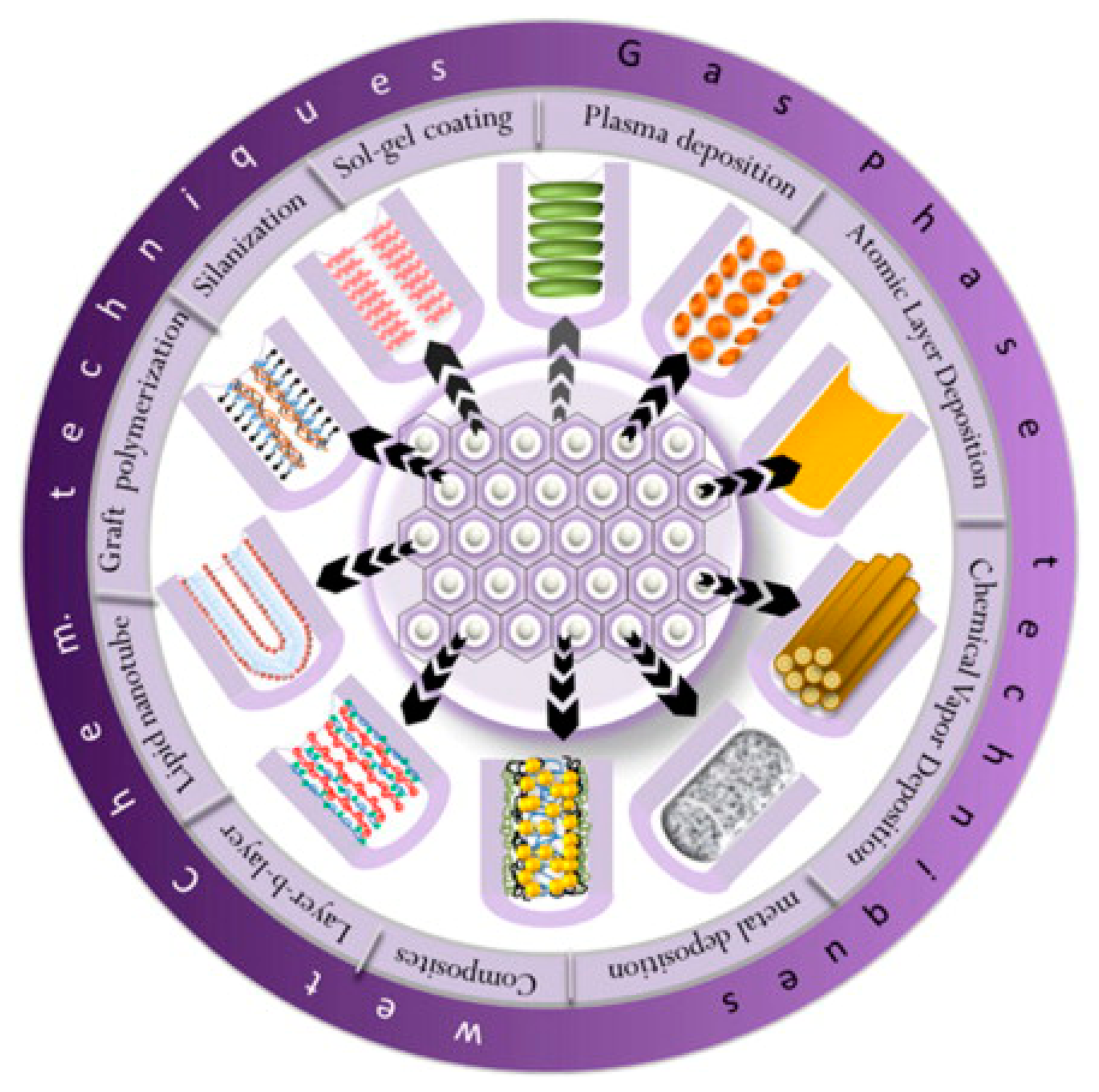


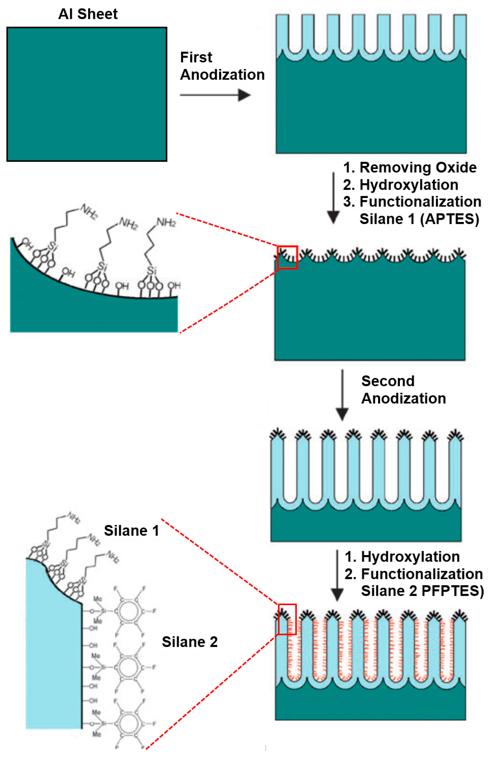


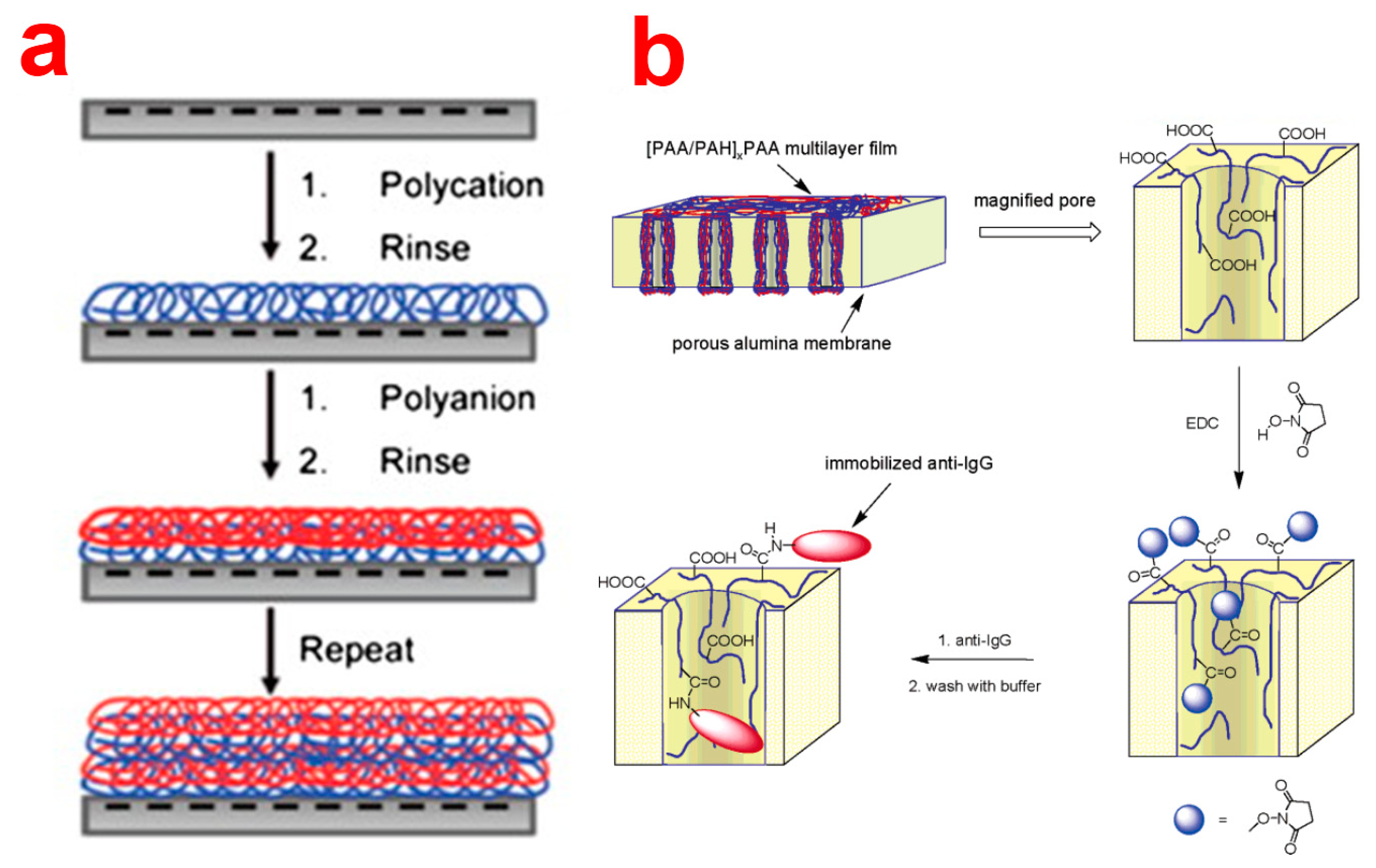


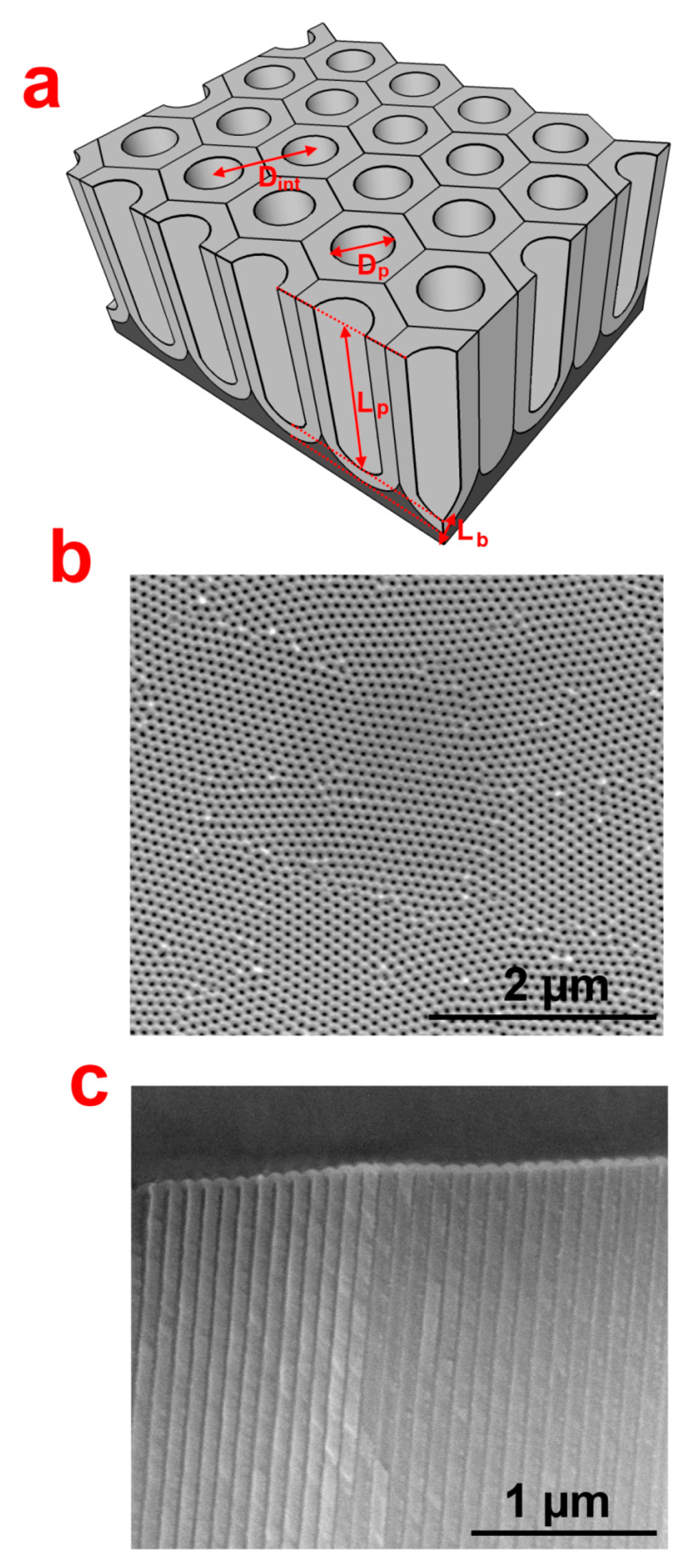
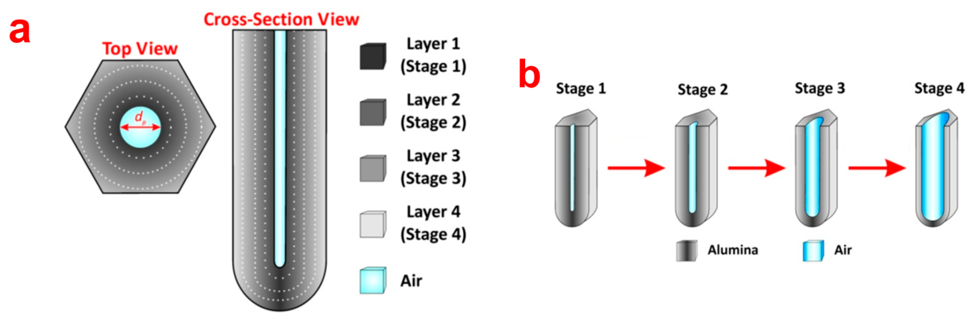
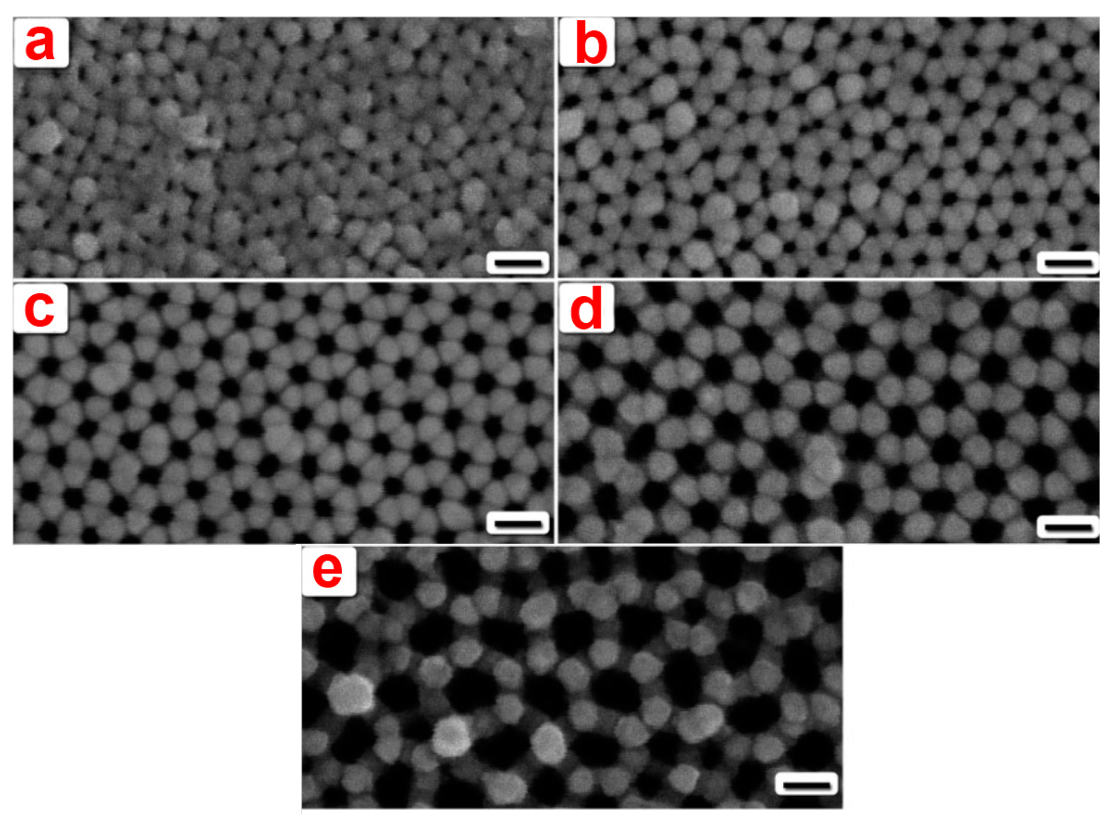
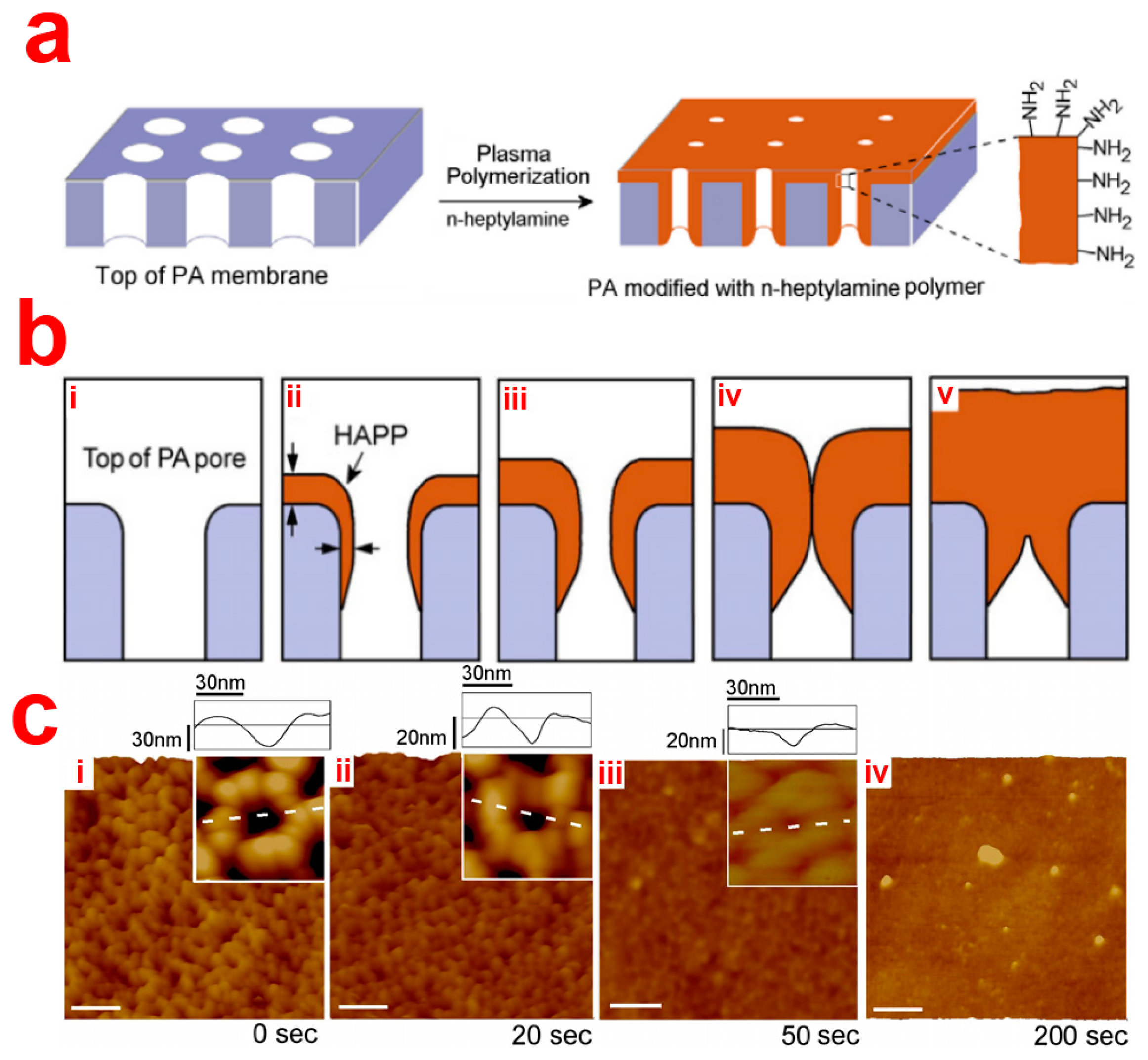
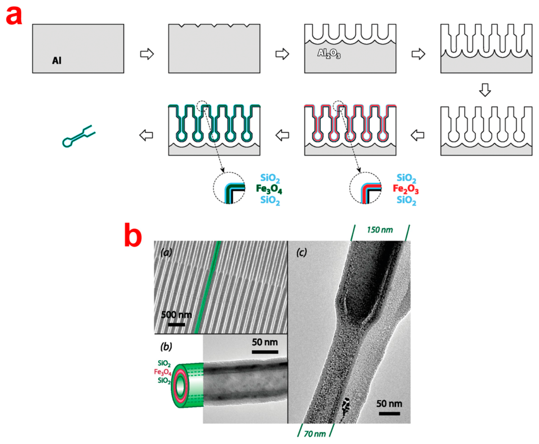
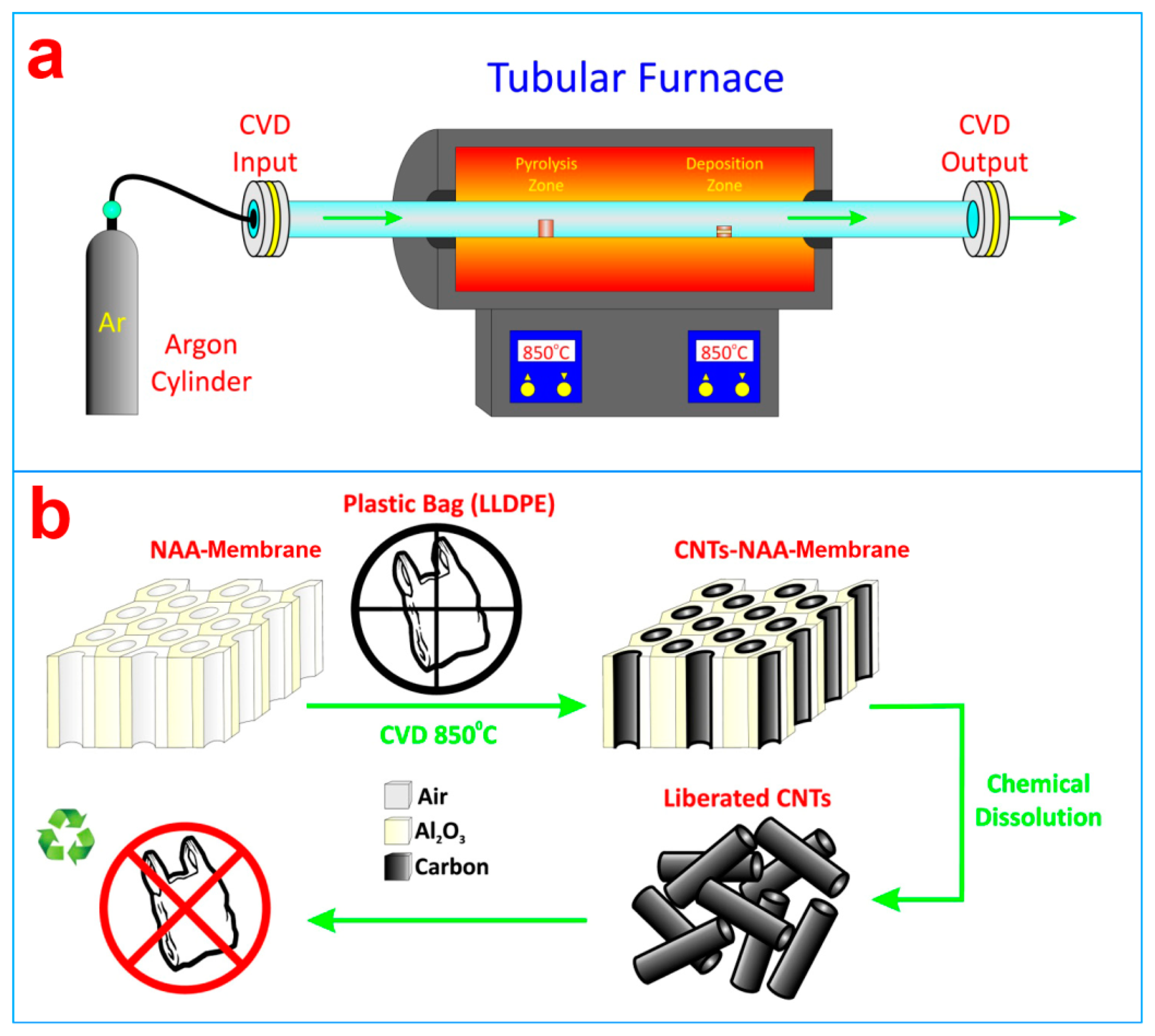
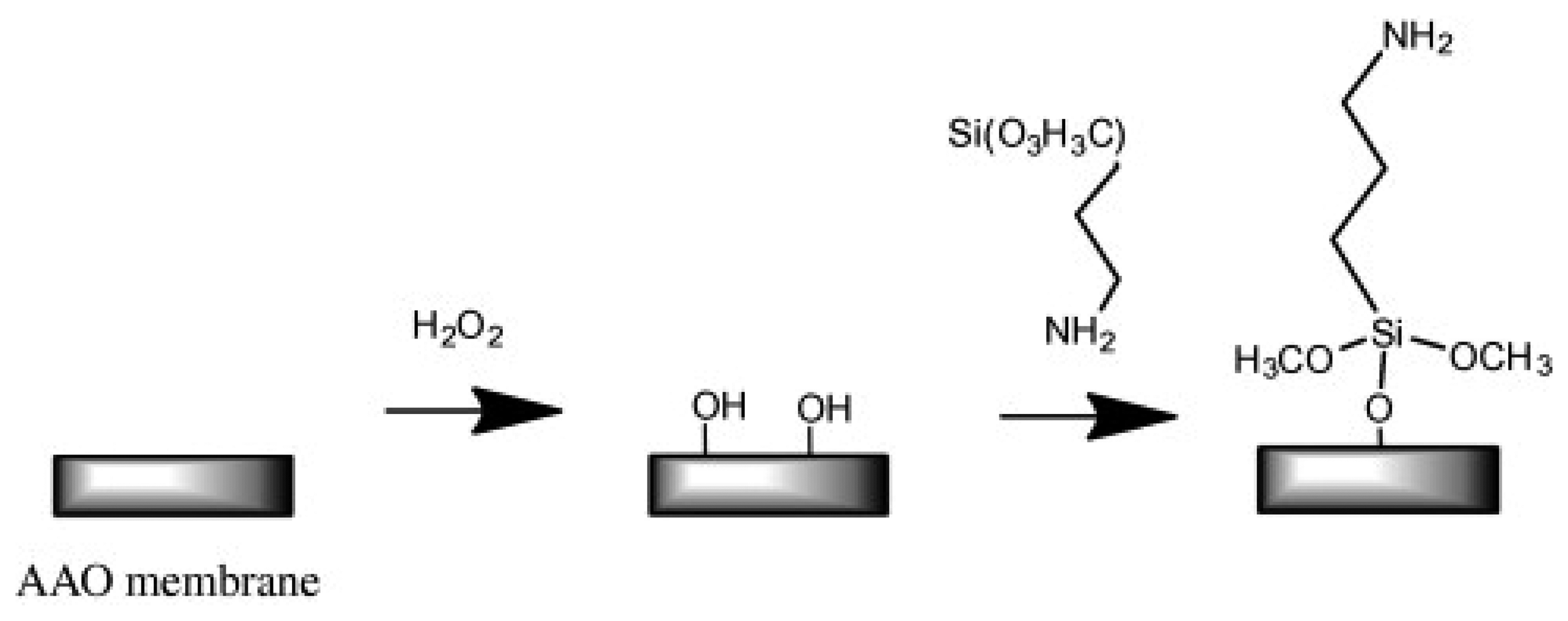
| Acid Electrolyte | Mild Anodization | Hard Anodization | ||||||
|---|---|---|---|---|---|---|---|---|
| T (°C) | V (V) | Dp (nm) | Ref. | T (°C) | V (V) | Dp (nm) | Ref. | |
| H2SO4 0.3 M | 5 | 25 | 25 | [15] | 0 | 40 | 30 | [23] |
| H2C2O4 0.3 M | 5–8 | 40 | 30 | [14] | 0–1 | 140 | 50 | [8] |
| H3PO4 0.1 M | 0–1 | 195 | 160 | [16] | ||||
| H3PO4:C2H5OH: H2O (1:20:79 v/v) | −10 to 0 | 195 | 80–140 | [9] | ||||
| Types | Silane Name | Modification Method | Application(s) | Ref. |
|---|---|---|---|---|
| Amino-silane | Aminopropyl-triethoxy silane | Solution based | Immobilization | [29,58] |
| PEG-silane | mPEG-silane | Solution based | Hydrophylization | [65–67] |
| Fluorinated-silane | perfluoroalkyl-silanes | Solution based | Transporting and separation | [5] |
| Mercapto-silane | Mercaptopropyl-triethoxy silane | CVD based | Sensing | [59] |
© 2014 by the authors; licensee MDPI, Basel, Switzerland This article is an open access article distributed under the terms and conditions of the Creative Commons Attribution license ( http://creativecommons.org/licenses/by/3.0/).
Share and Cite
Kumeria, T.; Santos, A.; Losic, D. Nanoporous Anodic Alumina Platforms: Engineered Surface Chemistry and Structure for Optical Sensing Applications. Sensors 2014, 14, 11878-11918. https://doi.org/10.3390/s140711878
Kumeria T, Santos A, Losic D. Nanoporous Anodic Alumina Platforms: Engineered Surface Chemistry and Structure for Optical Sensing Applications. Sensors. 2014; 14(7):11878-11918. https://doi.org/10.3390/s140711878
Chicago/Turabian StyleKumeria, Tushar, Abel Santos, and Dusan Losic. 2014. "Nanoporous Anodic Alumina Platforms: Engineered Surface Chemistry and Structure for Optical Sensing Applications" Sensors 14, no. 7: 11878-11918. https://doi.org/10.3390/s140711878