Design, Experiments and Simulation of Voltage Transformers on the Basis of a Differential Input D-dot Sensor


Abstract
: Currently available traditional electromagnetic voltage sensors fail to meet the measurement requirements of the smart grid, because of low accuracy in the static and dynamic ranges and the occurrence of ferromagnetic resonance attributed to overvoltage and output short circuit. This work develops a new non-contact high-bandwidth voltage measurement system for power equipment. This system aims at the miniaturization and non-contact measurement of the smart grid. After traditional D-dot voltage probe analysis, an improved method is proposed. For the sensor to work in a self-integrating pattern, the differential input pattern is adopted for circuit design, and grounding is removed. To prove the structure design, circuit component parameters, and insulation characteristics, Ansoft Maxwell software is used for the simulation. Moreover, the new probe was tested on a 10 kV high-voltage test platform for steady-state error and transient behavior. Experimental results ascertain that the root mean square values of measured voltage are precise and that the phase error is small. The D-dot voltage sensor not only meets the requirement of high accuracy but also exhibits satisfactory transient response. This sensor can meet the intelligence, miniaturization, and convenience requirements of the smart grid.1. Introduction
The accuracy, convenience, and rapid response of a voltage transformer serve an important function in power system fault analysis, power system monitoring, and electric energy measurement of smart grid. Potential transformers (PTs) and capacitive voltage transformers (CVTs) are commonly used in high-voltage and extra-high-voltage grids in China. However, PTs are confronted with problems like large volume and increasing insulation difficulty as voltage grade increases [1]. Compared with PTs, CVTs have more advantages due to their simple insulation structure and high performance-price ratio. However, CVTs have poor transient responses because they contain coupling capacitances, intermediate transformers, compensation reactors, and other energy storage elements. Moreover, high-frequency oscillation caused through ferroresonance easily occurs on the secondary side, which will threaten the safe operation of the apparatus [2]. Optical voltage transformers (OVT) based on the Pockels Effect have numerous advantages, such as high measuring accuracy, good safety, and avoidance of electromagnetic field interference, however, changes of external temperature significantly affect the reliability and measurement accuracy of OVTs. Moreover, OVTs based on the Pockels Effect have the disadvantage of a nonlinear problem in photoelectric conversion [3].
1.1. Traditional D-Dot Voltage Sensor
The D-dot output voltage signal is proportional to the first-order micro component of the electric displacement vector in the space of sensor to time Ḋ or εdE/dt;, which is thus called a D-dot voltage sensor. Traditional D-dot voltage sensors based on the electric field coupling principle can be used to measure high voltage levels of up to 220 kV in theory. A D-dot sensor has a simple structure, as shown in Figure 1. Thus, the frequency response of such sensor is equal to a first-order RC circuit [4].The circuit component parameters are needed for adjustment until the bandwidth satisfies the measurement range from several Hertz to 6 × 10⁵ Hz, which is significantly larger than that of a traditional voltage sensor [5].
Principle of the Traditional D-Dot Sensor
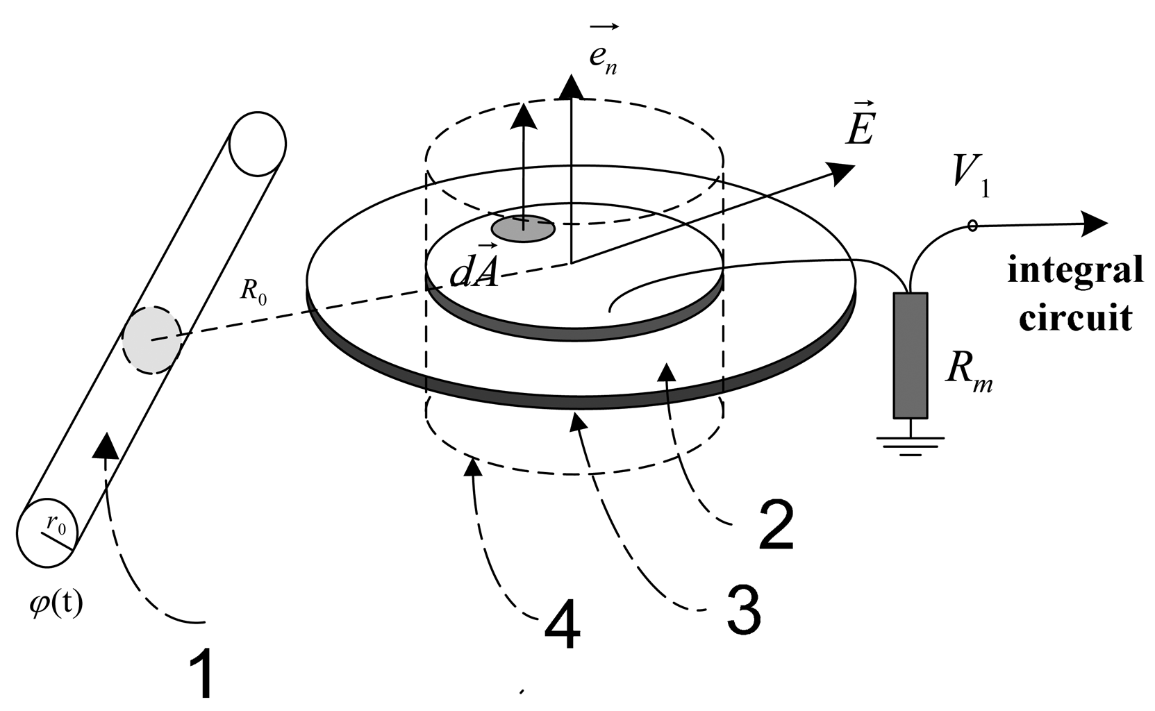
Figure 1 shows the structural diagram of a traditional D-dot voltage sensor. Part 1 of Figure 1 shows the measured wire. Part 2 of Figure 1 shows the metal conductor with high electrical conductivity. Part 3 of Figure 1 shows the grounding insulation. Part 4 of Figure 1 shows the closed gauss surface, which is not a physical part of the sensor. The traditional D-dot voltage sensor incorporates the grounded insulator and measuring resistance Rm. The insulator connects to a coaxial cable and a metal conductor with high electrical conductivity. The electrode near the measured conductor 1 can induce the charge on the basis of the electric field coupling principle [6]. A closed Gaussian surface exists on the metal conductor surface. Gauss' theorem is applied to the closed Gaussian surface:
When the changed induced charge flows through the measuring resistor, such a charge will generate the resistive voltage drop V1(t) on the measuring resistor. As a result, the measured wire potential φ(t) becomes proportional to the electric field intensity of the sensor measuring point [7–9]. Thus, the relationship between the single electrode and measured voltage is:
Thus, the wire voltage is given by:
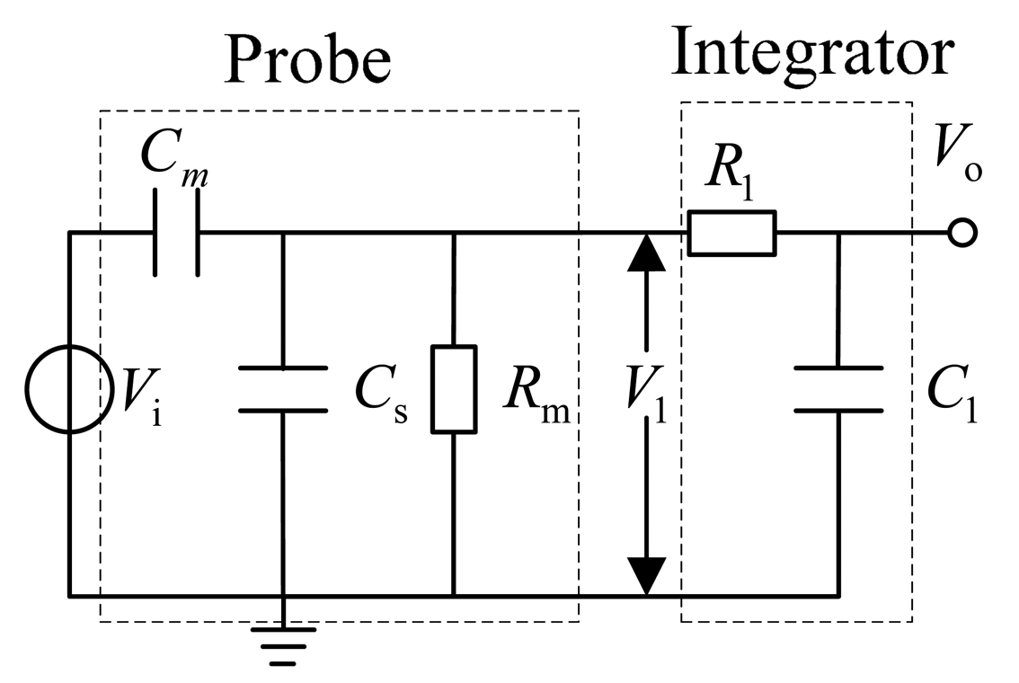
The D-dot output signal V1(t) should be integrated into Equation (3) to obtain the time domain waveform. Figure 2 shows the equivalent measurement circuit of the traditional D-dot voltage sensor [10].
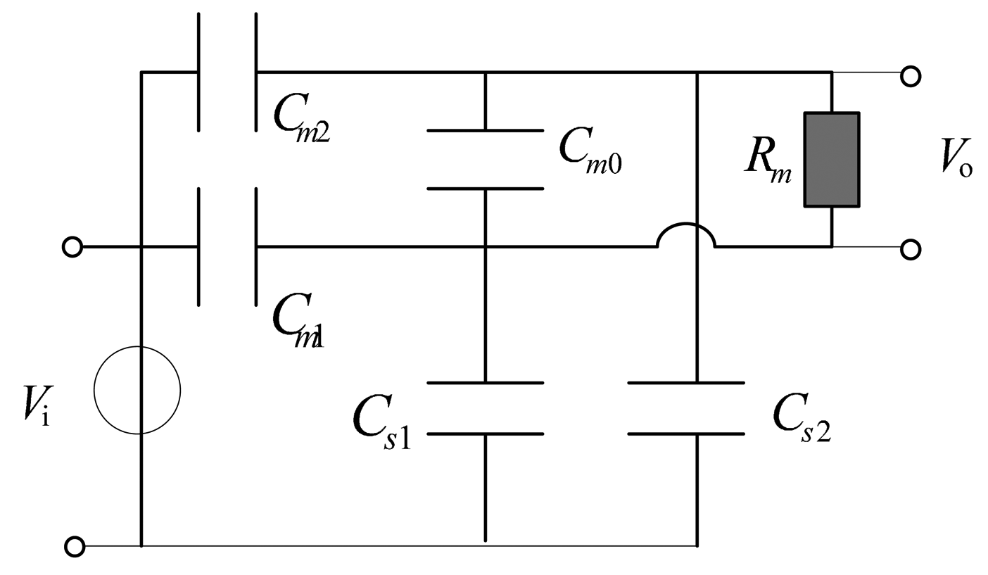
In Figure 2, Vi is the measured voltage, Cm is the equivalent mutual capacitance between the sensor and measured wire, and Cs is the equivalent stray capacitance between the sensor and the earth [11]:
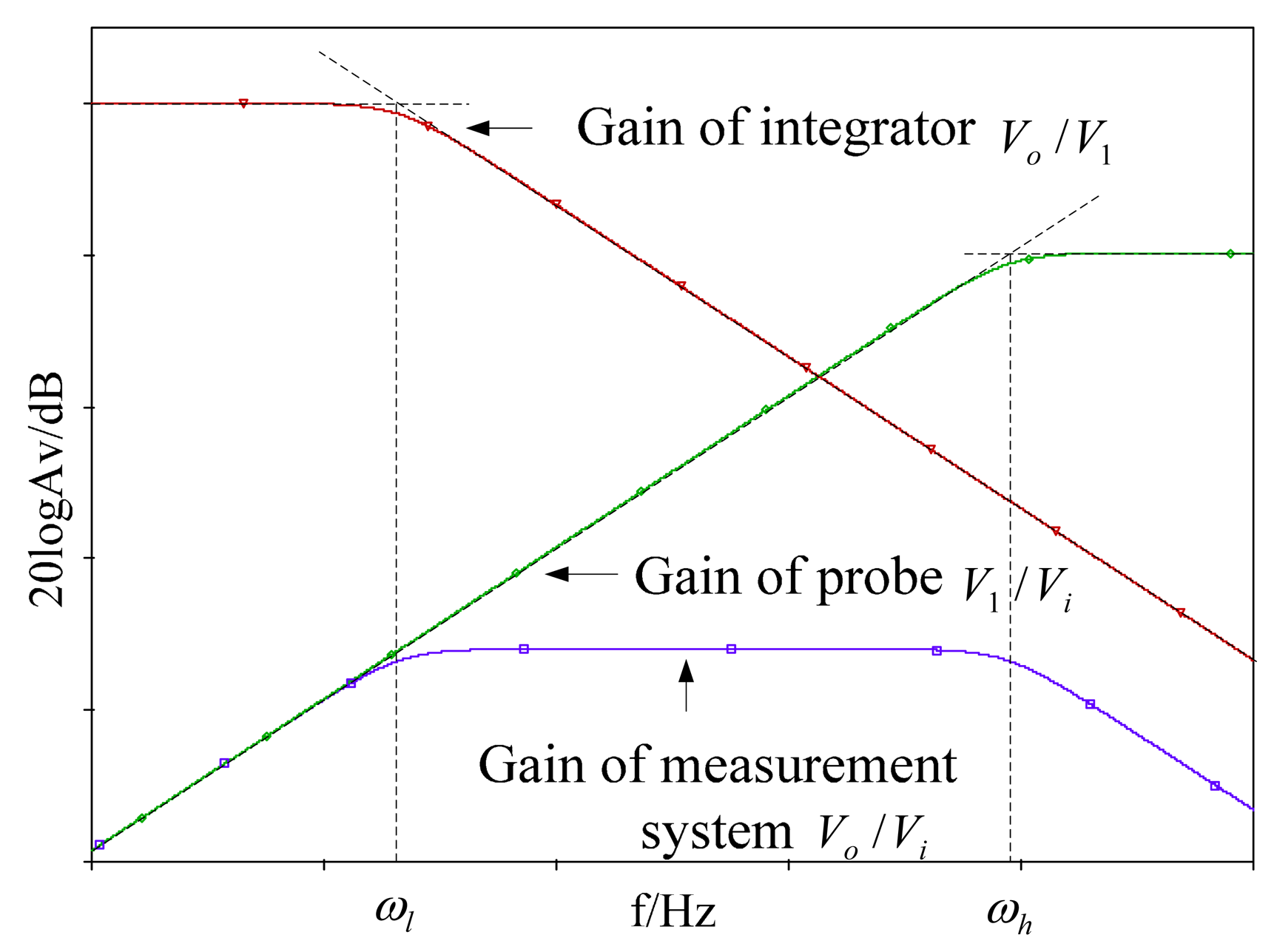
Thus, traditional D-dot sensor will work in a differential pattern. Figure 3 shows the Bode plot of the traditional D-dot probe [12].
In Figure 3, the upper limit of the D-dot measurement bandwidth is restricted by the angular frequency of the D-dot measuring circuit, whereas the lower limit of the D-dot measurement bandwidth is restricted by the angular frequency of the D-dot integration circuit [13,14]. The use of an integrator hinders the improvement of the signal-to-noise ratio of the sensor. Meanwhile, the waveform is distorted by the stray parameter of the integrator [15].
1.2. Improved Differential Input of D-Dot Sensors
For the sensor to work with a self-integrating pattern, the differential input pattern is adopted for circuit design. The differential voltage signal is obtained by measuring the floating potential difference of both ends of the electrode. Grounding is then removed. Figure 4 shows the new-designed differential D-dot sensor that can measure the grid power line without contact and the need of ground insulation where Cm2 and Cm1 are the mutual capacitances between the annular electrode and measured transmission conductor, Cs1 and Cs2 are stray capacitances between two annular electrodes and the earth Cm0 is the mutual capacitance of two annular electrodes, and Rm is the input equivalent resistance of the differential amplifier for measurement.
The transfer function, amplitude-frequency characteristic of the improved D-dot sensor are given by the following expressions.
The transfer function is:
The amplitude-frequency characteristic is:
The phase-frequency characteristic is:
In conclusion, the traditional D-dot voltage sensor has been improved. The differential input D-dot sensor can not only add the frequency bandwidth, but also avoid actual electrical connection with the ground electrode from input to output, thus preventing the damage to the secondary side when grounding current flows through the measurement system. The problem of ground insulation will not necessarily be aconcern. The new and improved D-dot sensor also has the advantages of miniaturization and non-contact digital measurement.
1.3. Model Design and Simulation of Improved D-dot Sensor
Model Design of the D-Dot Sensor
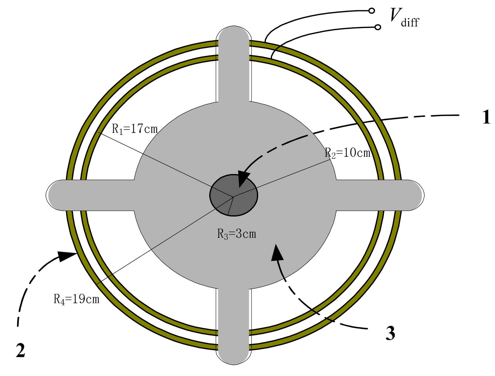
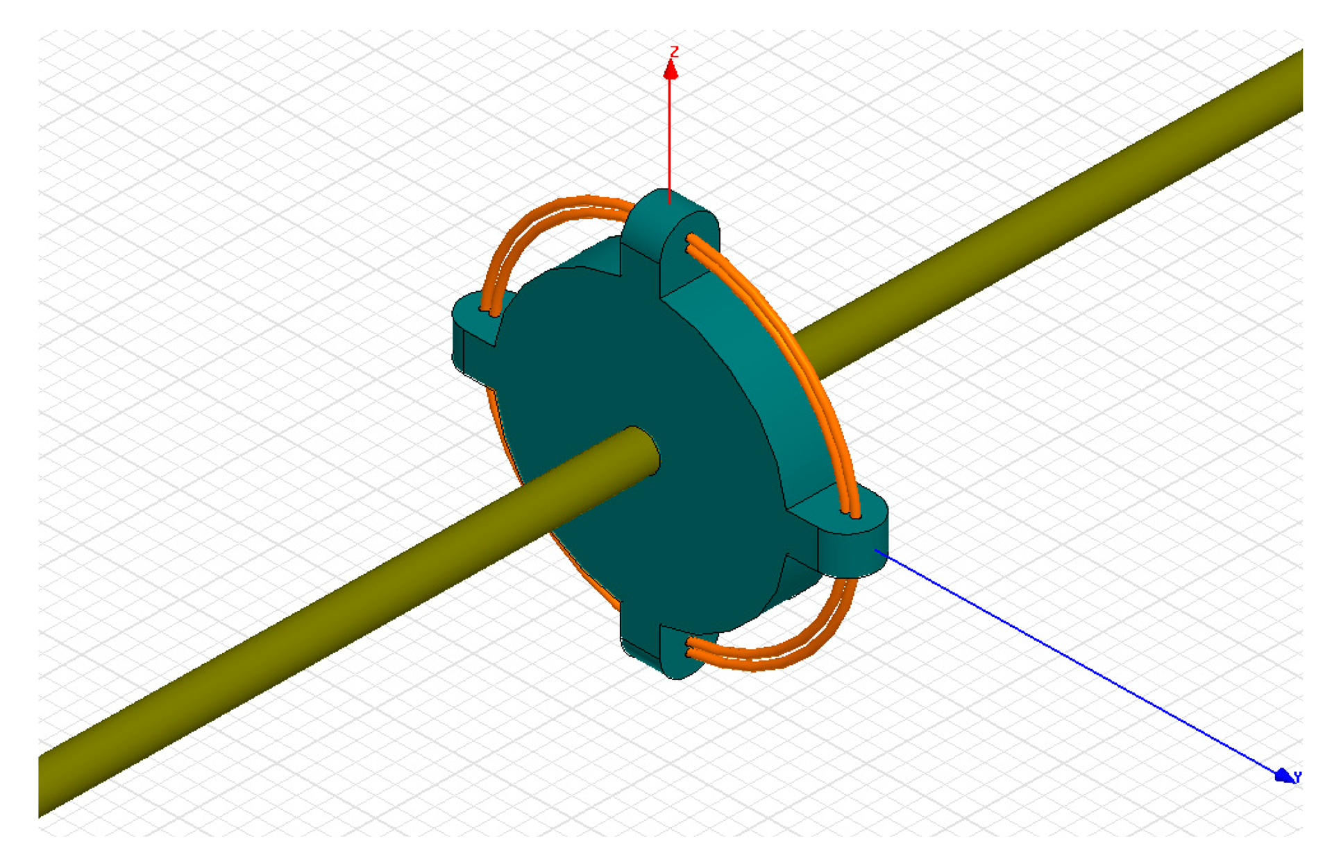
Figure 5 shows the hardware architecture of the improved D-dot sensor. This architecture mainly consists of an inner copper ring, an exterior copper ring, and an insulating support. The inner and exterior copper rings are concentric annuli of different radii. The rings are both fixed on the insulation support. A through hole is used to fix the measured wire onto the insulating support, which is made of epoxy resin with added E-type fiberglass. The two copper rings can be considered as two D-dot sensors with different Aεq. Epoxy resin not only supports the whole sensor structure, but also reduces the influence of the external electric field owing to its good insulation characteristic (the electric breakdown strength of E-type fiberglass epoxy resin is 35,000 kV/m). Finally, the insulation capability of the entire sensor is improved, and output power is reduced to satisfy the miniwatt drive requirements for there lay protection of the power system and of the secondary measuring equipment.
where: 1 is the measured wire, 2 denotes the copper rings, and 3 is the epoxy resin support.
2. Simulation of Improved D-Dot Sensor
2.1. Circuit Simulation of the Improved D-Dot Sensor
Through the optimization function of Ansoft Maxwell, the values of Cm0, Cm1, Cm2, Cs1, and Cs2 can be calculated. The specific values are shown in Table 1.
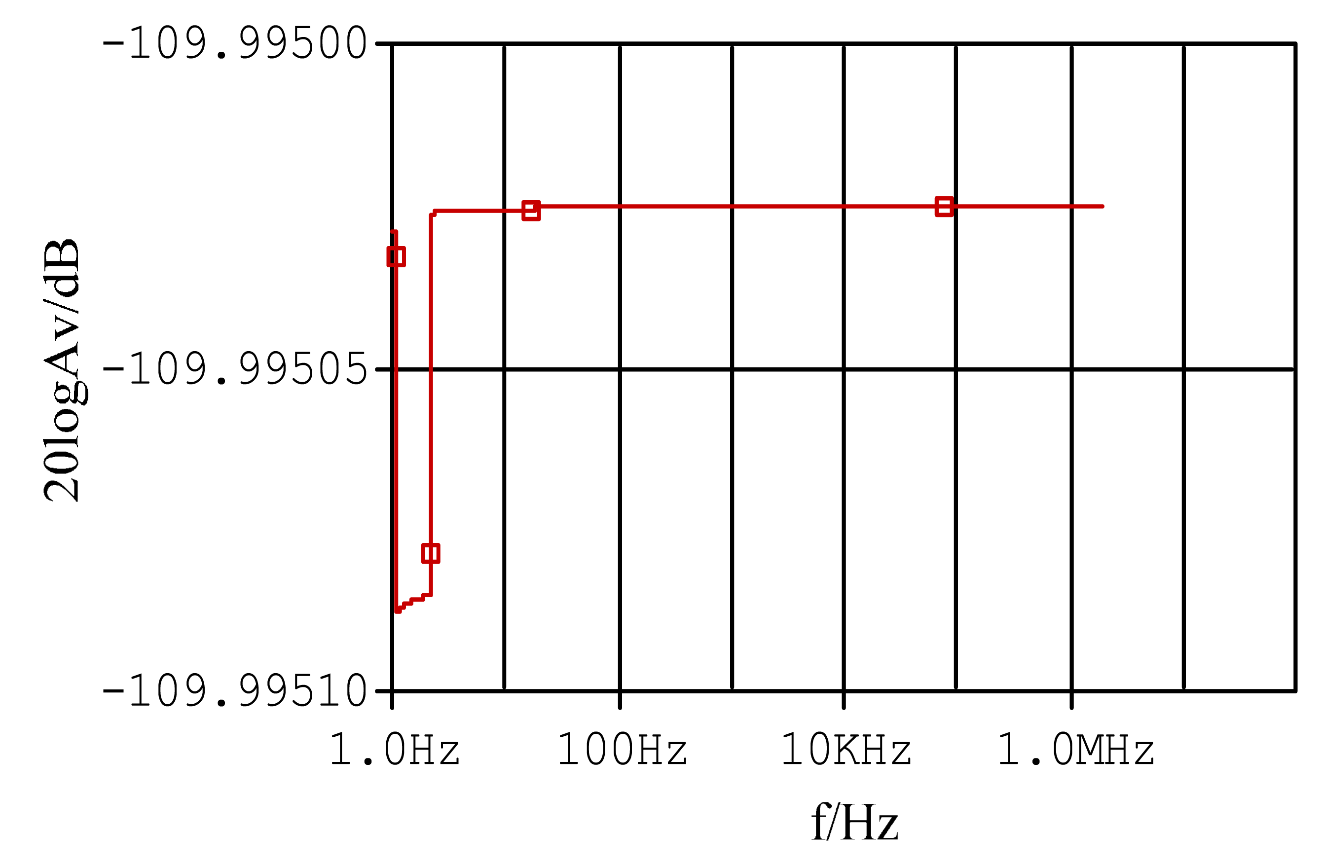
PSpice simulation software is used to prove that the measurement of the improved sensor has greater bandwidth than previously achieved. Figure 6 shows that steady gain can be sustained with a large bandwidth.
2.2. Simulation Model
Figure 7 shows the 3D finite element model established by the electromagnetic simulation software Ansoft Maxwell. The modeling steps are given below.
The excitation source can be approximated to an infinitely long transmission line, and the electric field vector is set to 0 at infinity from the excitation source when considering the actual operating conditions of the sensor [16]. Thus, the calculation method for expanding the electric field area is employed to solve the open electric field problem. For the model of the D-dot sensor, the distribution of the electric field is axisymmetric. Thus, so the cylindrical coordinate system (r,φ,z) is adopted. In this system, r is the coordinate of radius, φ is the azimuth angle, and z is the symmetry axis coordinate. In the model, the half fields are chosen as the calculation field. In the whole calculation field of the model, the potentiometric function satisfies the following differential equation [17]:
The critical region between the epoxy resin structure of the D-dot sensor and external air satisfy the equations:
2.3. Results and Analysis of Simulation
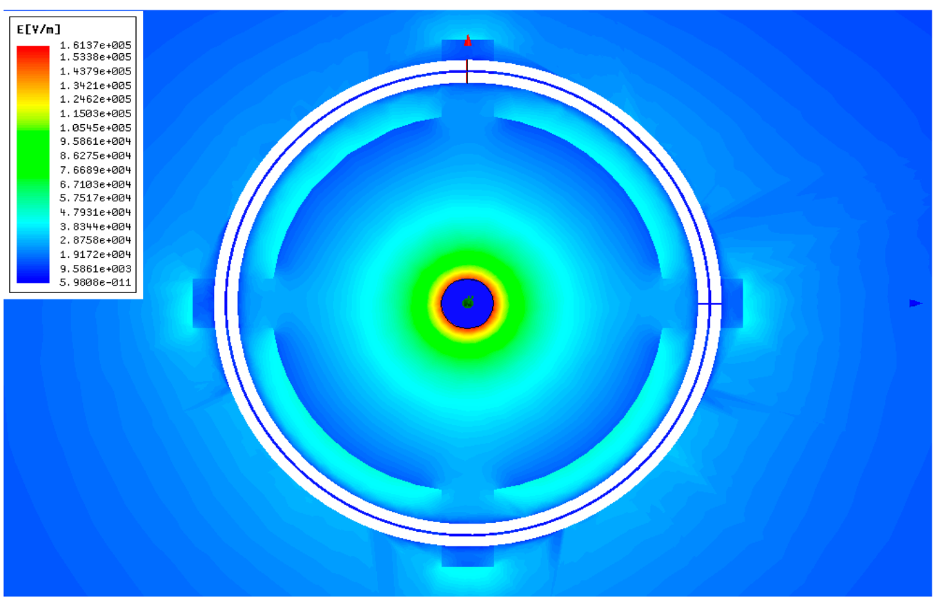
To demonstrate the feasibility of the structural design and material selection of the D-dot voltage sensor and to solve the problems of electric field distortion and ground insulation, the electric field distribution curves around the sensor at a 10 kV power frequency voltage are simulated.
The electric field intensity inside the sensor decreases with increasing distance, as shown in Figure 8. In addition, the linearity of the relation curves between electric field intensity and distance is relatively ideal, which indicates that the influence from the sensor with the highest electric field intensity inside the epoxy resin support is 161.37 kV/m. This value is significantly smaller than the breakdown strength of epoxy resin. This finding demonstrates that the material and structural design of the support will not be broken down by a high electric field, thus improving the insulating strength of the sensor.
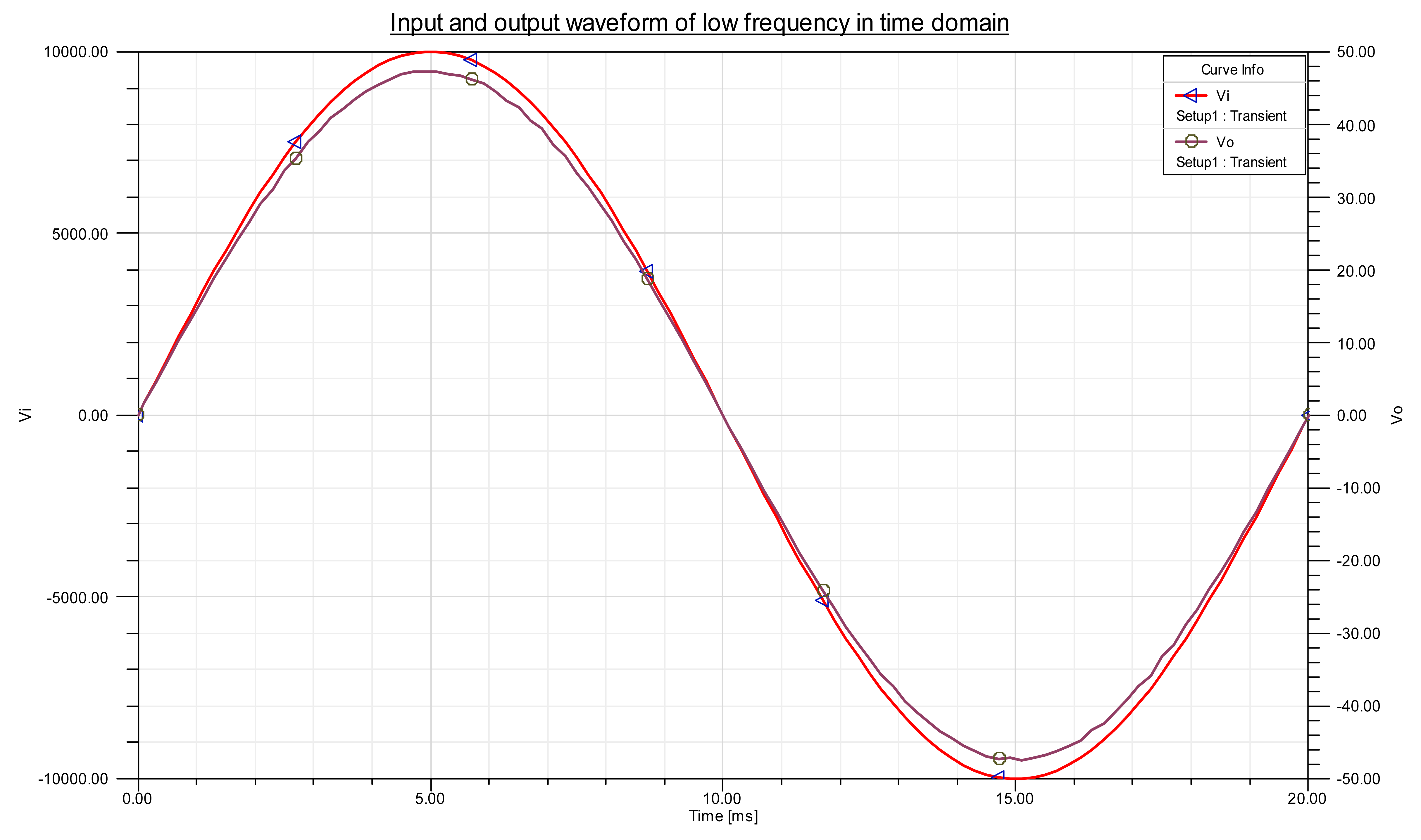
To demonstrate that the improved sensor has no phase delay in steady state, the time domain waveforms of the input and output sensors at 50 Hz sine excitation are simulated. In Figure 9, Vi is the measured voltage, whereas Vo is the output voltage of the sensor. As shown in Figure 9, almost no phase delay exists between Vi and Vo.
3. Performance Test and Data Analysis of Sensor
After designing and establishing the D-dot voltage sensor model, the steady-state error and transient response experiments are conducted to evaluate model performance.
The high-voltage test platform is shown in Figure 10. The voltage control box controls the power frequency voltage output. The transformer connects to a long straight copper rod that is taken as a single-phase transmission wire [19,20]. The high-voltage probe, which has a compensating circuit, is used to measure the voltage of the wire, which goes through the center of the sensor. The relative amplitude of the waveforms will be compared on the oscilloscope by measuring the waveform of the output voltage of the sensor and the wire simultaneously. The polder model is employed for the measurement oscilloscope. This model can mitigate the interference signal and improve electromagnetic compatibility. The attenuation ratio of the high-voltage probe is 1000:1, and the probe type is a Tektronix P6015A. The base and vertical accuracies are 0.75% and 1.5%, respectively. This probe can rectify and compensate the measured voltage to eliminate measurement errors. Therefore, the output of this probe can be used as standard contrast signal of the experiment.
3.1. Steady-State Error Experiment
A voltage of 10 kV is used as the standard measuring voltage, and the transformer is controlled for the wire voltage to reach 10%, 20%, 50%, 80%, 100%, and 120% of 10 kV to measure the output voltage of the high-voltage probe and sensor. Subsequently, the output voltage values are calculated to determine the ratio error. As shown in Table 2, UHV is the voltage of the high-voltage probe, which is converted to the primary side; and UD-dot is the measured sensor voltage.
where Ratio Error (ε%) is given by .
The diagram below is based on a 10 kV power frequency voltageand depicts acomparison of the voltage waveform between a high-voltage probe (CH2, blue) and that of sensor (CH1, yellow) when the wire is applied with a phase voltage of 10 and 5 kV successively. In Figures 11 and 12:
Figures 11 and 12, as well as Table 2, illustrate that:
The measured voltage in Table 2 has been fitted once, and its square error is 0.014, which indicates that the sensor can maintain a linear input-output trait within the range of 10% to 120% Un and has a satisfactory dynamic range.
Table 2 shows that within the range of 10% Un to 120% Un, the ratio error is less than 1%, which proves that the sensor precision is relatively high and that the RMS value error is relatively small.
Figures 11 and 12 illustrate that the error of the waveform phase of the sensor and high-voltage probe, as well as the degree of waveform distortion, is very small.
As seen from Table 2, the transformation ratio of the D-dot sensor is approximately 1:2203.
3.2. Experiments of Transient Response
The D-dot sensor implements voltages through electric field coupling and does not contain inductive components. Therefore, the response of such sensor to the transient voltage waveform is relatively fast. An impulse voltage test is conducted to verify the transient performance of this sensor.
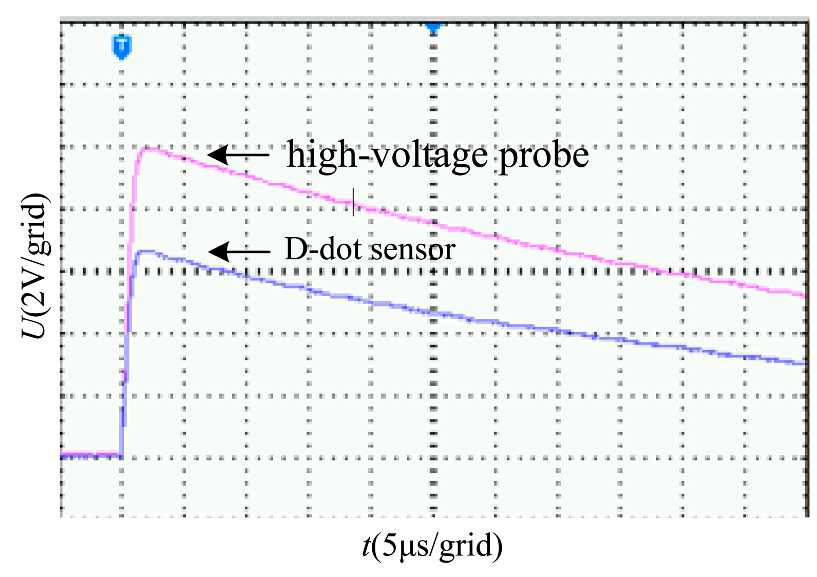
The 1.2/50 μs standard lightning impulse voltage is applied to the line with an impulsive voltage generator, and the signal measured by the sensor and high-voltage probe were displayed on the oscilloscope, as shown in Figure 13.
As shown in Figure 13, the D-dot voltage sensor exhibits rapid response speed while preventing the occurrence of high-frequency oscillation.
4. Conclusions and Outlook
A new kind of differential inputs D-dot voltage sensor was designed to measure the transmission line voltage. The designed model was theoretically analyzed and simulated. In addition, steady and transient state experiments were conducted. The simulation and experimental results indicate that the sensor possesses tiny steady-state error and excellent transient performance. In this method, no electrical connection exists between the sensor and transmission line. The new sensor achieves miniaturization as well as non-contact digital measurement and is not needed to be insulated against ground, adapting to the development of smart grid and offering a new approach for electric parameters measurement of power system.
In future research, the measuring error will be analyzed and electromagnetic interference, variation of temperature and relative humidity will be taken into consideration to make sure the sensor can effectively work in field operation. Furthermore, the decomposition problem of three-phase composite electric field will be researched to achieve three-phase voltage measurement.
Acknowledgments
This work was supported by the National Natural Science Foundation of China (Grant No. 51207175) and by the Scientific Research Foundation of SKL for Power Transmission Equipment & System Security and New Technology (2007DA10512713305). The authors thank all members of the external insulation research team of the College of Electrical Engineering, Chongqing University, for their hard work in obtaining the experimental data for this study.
Author Contributions
Jingang Wang developed and applied algorithm identification for joint angle measurement under the valuable guidance and advice of Jie Yang. Both contributed to the data acquisition for the experiments, which Can Gao conducted. Jingang Wang is the head of the research group that conducted this study. He contributed to the research through his general guidance and advice. All authors contributed to the writing andrevision ofthe manuscript.
Conflicts of Interest
The authors declare no conflict of interest.
References
- Pan, F.; Xiao, X.; Xu, Y.; Ren, S. An optical AC voltage sensor based on the transverse pockels effect. Sensors 2011, 11, 6593–6602. [Google Scholar]
- Wang, J.; He, W.; Li, Q.; Yang, F.; Yang, Y.; Chen, T. Non-contact electroscope for ultra-high-voltage appliances based on ultra-violet pulse detecting. Trans. China Electrotech. Soc. 2008, 23, 137–142. [Google Scholar]
- Rodríguez, A.; Bueno, E.J.; Mayor, Á.; Francisco, J.R.; Aurelio, G.-C. Voltage Support Provided by STATCOM in Unbalanced Power Systems. Energies 2014, 7, 1003–1026. [Google Scholar]
- Xiong, X.; Zhou, J.; Zhou, Y. A New Method of Correcting Transient Characteristics of Capacitive Voltage Transformer Using Principle of Superposition. Trans. China Electrotech. Soc. 2006, 22, 107–111. [Google Scholar]
- Liu, F.; Bi, W.; Wang, J. Structure of Sensor Head for Optical High Voltage Transducer. Trans. China Electrotech. Soc. 2008, 16, 43–48. [Google Scholar]
- Yu, M.; Wang, J.; Ma, J.; Peng, H.; Xiong, L. Research on Non-contact Voltage Transducer for High-Voltage Transmission Lines Based on Inverse Problem of Electric Field. Int. J. Emerg. Electric Power Syst. 2014, 15, 101–109. [Google Scholar]
- Struve, K.W.; Horry, M.L.; Spielman, R.B. Design calibration, and performance of water diagnostics on the PBFA Z. Proceedings of 1997 11th IEEE International Pulsed Power Conference, Baltimore, MD, USA, 29 June–2 July 1997; pp. 1303–1308.
- Yang, F. Study on Forward and Inverse Problem of Power Frequency Electric Field of Transmission and Distribution Apparatuses and Power Frequency Electromagnetic Environment. Ph.D. Thesis, Degree of Engineering, Chongqing University, Chongqing, China, 2008. [Google Scholar]
- Feng, J.-Q.; Wang, Q.-M.; Ding, F.-L.; Qiao, Z. Present Research Situation and Trend of Electronic Voltage Transformer. Transformer 2010, 47, 40–43. [Google Scholar]
- Wang, D.; Wang, X. A Study of the Protective Device with Inductor in Series Resistance for Capacitor Voltage Transformer. Trans. China Electrotech. Soc. 2009, 22, 41–46. [Google Scholar]
- Hou, D.; Roberts, J. Capacitive voltage transformer: Transient overreach concerns and solutions for distance relaying. Proceedings of IEEE Canadian Conference on Electrical and Computer Engineering, Calgary, Alta., AB, Canada, 26–29 May 1996; pp. 119–125.
- Xia, M.; Li, X. Design and Implementation of a High Quality Power Supply Scheme for Distributed Generation in a Micro-Grid. Energies 2013, 6, 4924–4944. [Google Scholar]
- Wagoner, T.C.; Stygar, W.A.; Ives, H.C.; Gilliland, T.L.; Spielman, R.B.; Johnson, M.F.; Reynolds, P.G.; Moore, J.K.; Mourning, R.L.; Fehl, D.L. Differential-output B-dot and D-dot monitors for current and voltage measurements on a 20-MA, 3-MV pulsed-power accelerator. Phys. Rev. Special Top.-Accelerators Beams 2008, 11. doi: http://dx.doi.org/10.1103/PhysRevSTAB.11.100401. [Google Scholar]
- Li, W. Study of Sensor Theory Centered on Rogowski Coil for Heavy Current Measurement Application for Heavy Current Measurement Application. Ph.D. Thesis, Hua Zhong University of Science and Technology, Wuhan, China, 2005. [Google Scholar]
- Lu, Q.Y.; Hu, W.; Zheng, L.; Min, Y.; Li, M.; Li, X.-P.; Ge, W.-C.; Wang, Z.-M. Integrated coordinated optimization control of automatic generation control and automatic voltage control in regional power grids. Energies 2012, 5, 3817–3834. [Google Scholar]
- Fang, C.; Li, W.; Wang, J.; Yu, J.; Cheng, C.; Hou, X. 10 kV Electronic Voltage Transformer Based on Resistor Divider. Trans. China Electrotech. Soc. 2007, 22, 58–63. [Google Scholar]
- Reinhard, M. Experimental Research on Single-Impulse Energy Handling Capability of MO-Varistors Used in High-Voltage Systems in Consideration of a Complex Failure Criterion. Ph.D. Dissertation, Darmstadt University of Technology, Hesse Darmstadt, Germany, 2009. [Google Scholar]
- Metwally, I.A. Comparative measurement of surge arrester residual voltages by D-dot probes and dividers. Electric Power Syst. Res. 2011, 81, 1274–1282. [Google Scholar]
- Yarovoy, A.; De Jongh, R.; Ligthart, L. Ultra-wideband sensor for electromagnetic field measurements in time domain. Electron. Lett. 2000, 36, 1679–1680. [Google Scholar]
- Moradzadeh, M.; Boel, R.; Vandevelde, L. Anticipating and Coordinating Voltage Control for Interconnected Power Systems. Energies 2014, 7, 1027–1047. [Google Scholar]


| Cm1/pF | Cm2/pF | Cs1/pF | Cs2/pF | Cm0/pF |
|---|---|---|---|---|
| 17.6425 | 15.7360 | 69.5856 | 94.0904 | 5631 |
| Measuring Point | UHV/kV | UD-dot/V | Ratio Error(%) |
|---|---|---|---|
| 10% Un | 0.99 | 0.453 | 0.90 |
| 20% Un | 2.00 | 0.915 | 0.75 |
| 50% Un | 4.98 | 2.29 | 0.52 |
| 80% Un | 8.02 | 3.68 | 0.31 |
| 100% Un | 10.03 | 4.60 | 0.26 |
| 120% Un | 12.00 | 5.50 | 0.19 |
© 2014 by the authors; licensee MDPI, Basel, Switzerland. This article is an open access article distributed under the terms and conditions of the Creative Commons Attribution license ( http://creativecommons.org/licenses/by/3.0/).
Share and Cite
Wang, J.; Gao, C.; Yang, J. Design, Experiments and Simulation of Voltage Transformers on the Basis of a Differential Input D-dot Sensor. Sensors 2014, 14, 12771-12783. https://doi.org/10.3390/s140712771
Wang J, Gao C, Yang J. Design, Experiments and Simulation of Voltage Transformers on the Basis of a Differential Input D-dot Sensor. Sensors. 2014; 14(7):12771-12783. https://doi.org/10.3390/s140712771
Chicago/Turabian StyleWang, Jingang, Can Gao, and Jie Yang. 2014. "Design, Experiments and Simulation of Voltage Transformers on the Basis of a Differential Input D-dot Sensor" Sensors 14, no. 7: 12771-12783. https://doi.org/10.3390/s140712771