The Intersection of CMOS Microsystems and Upconversion Nanoparticles for Luminescence Bioimaging and Bioassays

 ,
,
Abstract
: Organic fluorophores and quantum dots are ubiquitous as contrast agents for bio-imaging and as labels in bioassays to enable the detection of biological targets and processes. Upconversion nanoparticles (UCNPs) offer a different set of opportunities as labels in bioassays and for bioimaging. UCNPs are excited at near-infrared (NIR) wavelengths where biological molecules are optically transparent, and their luminesce in the visible and ultraviolet (UV) wavelength range is suitable for detection using complementary metal-oxide-semiconductor (CMOS) technology. These nanoparticles provide multiple sharp emission bands, long lifetimes, tunable emission, high photostability, and low cytotoxicity, which render them particularly useful for bio-imaging applications and multiplexed bioassays. This paper surveys several key concepts surrounding upconversion nanoparticles and the systems that detect and process the corresponding luminescence signals. The principle of photon upconversion, tuning of emission wavelengths, UCNP bioassays, and UCNP time-resolved techniques are described. Electronic readout systems for signal detection and processing suitable for UCNP luminescence using CMOS technology are discussed. This includes recent progress in miniaturized detectors, integrated spectral sensing, and high-precision time-domain circuits. Emphasis is placed on the physical attributes of UCNPs that map strongly to the technical features that CMOS devices excel in delivering, exploring the interoperability between the two technologies.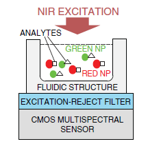
1. Introduction
Medical, environmental, and life science applications generate demands for low-cost small-size biochemical assay systems. These systems consist of bioassay chemistry and readout electronics responsible for analytical signal transduction and subsequent processing, respectively. The use of organic fluorophores as contrast agents for bio-imaging when coupled with appropriate selective biorecognition molecules enables visualization of biological processes. Although optical bio-imaging and bioassays that make use of fluorophores are common, these applications are not without limitations. Molecular fluorophores have broad emission spectra that render them unsuitable for implementation for higher densities of multiplexed biolabeling. They also often suffer from low sensitivity and photodegradation. Quantum dots that feature a large molar extinction coefficient, high quantum yield, narrow emission bandwidth, size-dependent tunable emission and high photostability are attractive as alternative fluorescent labels for optical labeling and imaging. However, the use of quantum dots for biological detection is limited by several factors. The potential toxicity of quantum dots that may pose risks to human health and the environment is a major drawback. Intermittent emission also limits their use for labeling individual biological molecules. In addition, both the organic fluorophores and quantum dots are generally excited with ultraviolet (UV) and visible light. Absorption of UV and visible light by the biological samples often induces autofluorescence, which interferes with fluorescent signals obtained from labeled exogenous biomarkers. Prolonged exposure of the biological samples to UV radiation can also cause sample photodamage and mutations [1].
The drawbacks of the Stokes-shifting dyes and quantum dots in biological applications have prompted the development of a new class of lanthanide-doped nanomaterials termed upconversion (UC) nanoparticles. UC nanoparticles, or UCNPs, exhibit anti-Stokes emission, and can be excited in the near-infrared (NIR) spectral region where biological molecules are generally optically transparent. In addition, these nanoparticles typically show sharp emission bands at a number of wavelengths, long lifetimes, tunable emission, high photostability, and low cytotoxicity, which render them particularly useful for bio-imaging and bioassay applications [1].
This paper surveys several key concepts surrounding upconversion nanoparticles and the systems that detect and process the luminescence signal. It is organized as follows. Section 2 describes the principle of photon upconversion, tuning of emission wavelengths, UCNP bioassays, and UCNP time-resolved techniques. Section 3 surveys the electronic readout system for signal detection and processing suitable for UCNP luminescence. The section describes the evolution and recent progress in miniaturized detectors, integrated spectral sensing, and high-precision time-domain circuits implemented in the complementary metal-oxide-semiconductor (CMOS) technology. Section 4 highlights key characteristics that result from combination of UCNPs and CMOS technology in a system. Throughout the paper, emphasis is placed on the physical attributes of UCNPs that map strongly to the technical features that CMOS devices excel in delivering, exploring the synergy between the two technologies.
2. Upconversion Nanoparticles
Advances in the ability to design the emission wavelength with a high degree of precision are the main driver for the recent interest in adoption of UCNPs. In this section, the principle of photon upconversion, optical tuning of the emission spectra of UCNPs, their application in bioassays, and their suitability for interrogation using time-resolved techniques are described.
2.1. Photon Upconversion
In contrast to conventional Stokes-type luminescence processes that are defined by a single ground- and a single excited-state, the UC process generates anti-Stokes emissions via the sequential absorption of two or more low-energy excitation photons through multiple, long-lived, metastable excited states. The various processes that lead to photon UC have recently been thoroughly reviewed, and the interested reader is directed elsewhere [1,2]. The anti-Stokes process is of interest as a mechanism to provide an analytical signal that is suitable for the development of optical assays and sensor technologies. The potential for excitation using low energy photons that are not strongly absorbed or scattered by biological and CMOS materials enables minimization of optical background interference, while the emission process can provide a wide spectral separation from the excitation wavelength.
Trivalent rare-earth lanthanide ions (Ln3+) have been implemented as dopants in various inorganic crystalline hosts such as NaYF4 to fabricate luminescent nanoparticles (NPs) with unique optical properties. The various synthetic strategies employed to fabricate these materials in a controlled fashion have recently been reviewed [1]. Such lanthanide doped NPs can exhibit optical down conversion (DC) as well as UC properties. DC refers to Stokes shifted emission where photons of lower energy are emitted, typically after excitation with radiation at the UV/blue part of the spectrum. UC refers to the anti-Stokes process where NPs absorb long-wavelength excitation radiation in the infrared (IR) or near-infrared region of the electromagnetic spectrum and emit photons of shorter wavelength, typically in a broad wavelength regime from UV to IR. The latter NPs are termed upconverting nanoparticles (UCNPs). Ln3+ ions are ideal candidates for photon UC since they possess long lived, metastable intermediate energy levels that are equally spaced and oriented in a ladder-type arrangement. The absorption and emission spectra of Ln3+ ions arise from Laporte forbidden 4f-4f electronic transitions. The shielding of these 4f electrons by the filled 5s2 and 5p6 subshells results in very narrow absorption and emissions bands from nanoparticles doped with these trivalent species [1]. Weak coupling between the crystal field of the host lattice and the f-f transition of the lanthanide ion means the emissions generated from a given lanthanide ion is nearly independent of the host material selected [3]. A wide variety of Ln3+ ions have been implemented in DC and UC systems [1]. Due to the involvement of spin-forbidden electronic transitions and anti-Stokes emissions, most lanthanide emissions should be more correctly referred to as luminescence rather than as fluorescence.
2.2. UCNP Structure and Optical Properties
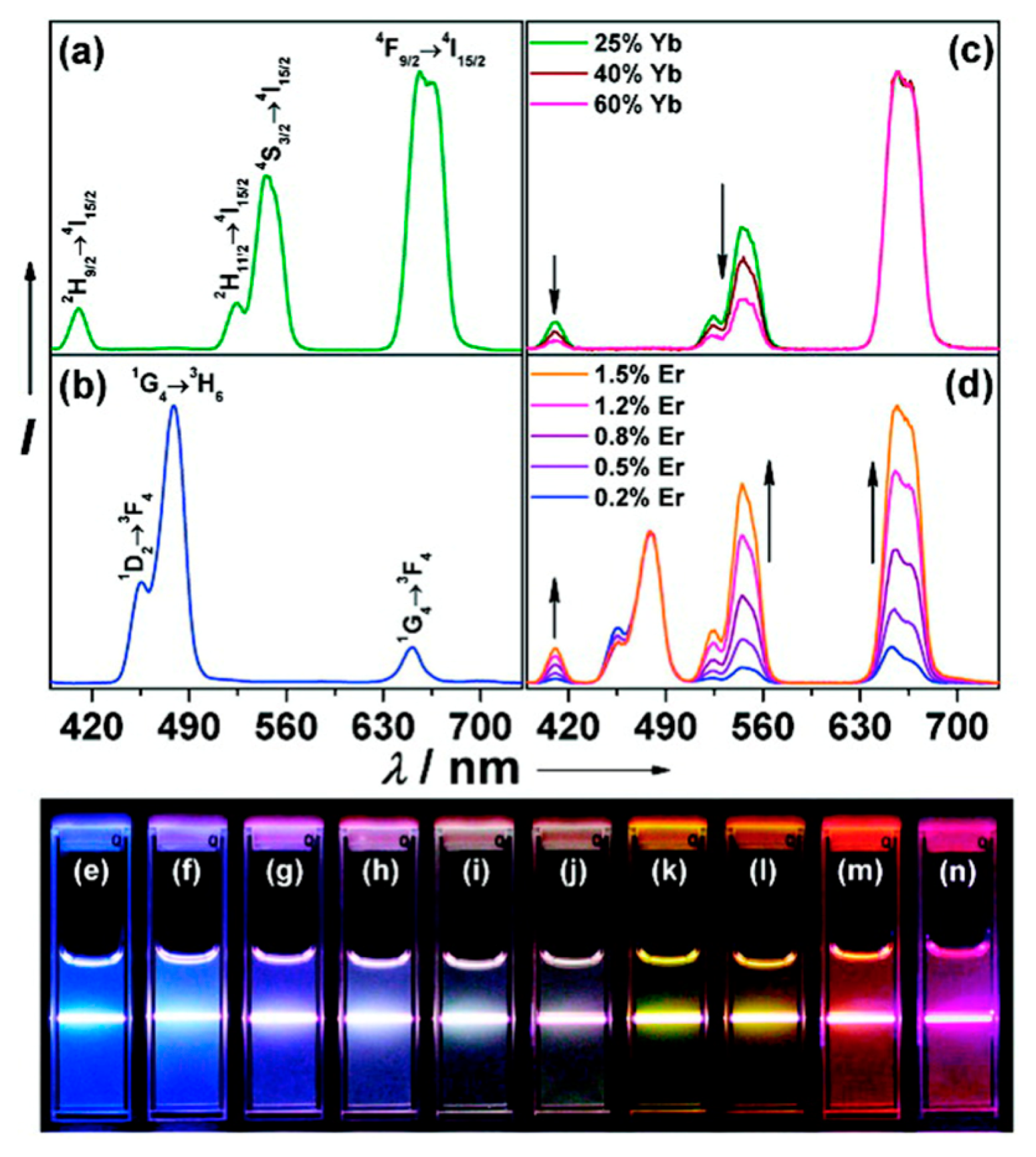
Luminescent UCNPs are typically comprised of an inorganic crystalline host material into which Ln3+ ions are embedded at low concentrations. The inorganic host is optically transparent and serves primarily as a scaffold orienting the optically active dopants appropriately in three-dimensional space. The architecture of UCNPs is typically in the form of core only, core-shell, or nanocomposite structures, each offering the potential to tune the optical properties of the resultant material. While many Ln+3 doped materials may exhibit NIR sensitized UC emissions, efficient and tunable UC luminescence is realized only for certain materials. Considerations for efficient UC emission in terms of architecture, host lattice choice, dopant ion selection, and dopant concentration have recently been presented [1]. In general, combinations of different lanthanide ions within the same material allows for some flexibility in the selection of emission wavelengths from an UCNP, due to the unique energy level structure of each lanthanide ion. By manipulating the identity and density of the dopants in a crystal matrix, and by combining more than one dopant ion in the host matrix, a variety of emissions from the NIR to the UV can be realized to tune the optical properties of these solid-state materials. Currently, the most common trivalent lanthanide emitters, or “activators”, used in UCNP systems are Tm3+, Er3+, and Ho3+. The emissions from these ions are efficiently “sensitized” by energy transfer from Yb3+, permitting multicolor emissions at a single excitation wavelength of 980 nm [1]. The emission spectrum of Tm3+ consists of a band at 800 nm, originating from the 3H4 → 3H6 transition, with two other higher energy bands in the violet and blue region with wavelengths 452 nm and 476 nm resulting from the 1D2 → 3F4 and 1G4 → 3H6 electronic transitions, respectively. The emission spectrum of Er3+ shows three distinct bands, two of which are centered in the green region of the visible spectrum at 525 and 545 nm, originating from the 2H11/2 → 4I15/2 and 4S3/2 → 4I15/2 electronic transitions, respectively, and one in the red region centered at 660 nm resulting from the 4F9/2 → 4I15/2 transition. For Ho3+, two main emissions bands are observed, one of which is green at 541 nm and one red at 647 nm, arising from the 5S2/5F4 → 5I8 and 5F5 → 5I8 electronic transitions, respectively [3]. Many strategies for optical tuning have been reported, and a classical effective approach was first disclosed by Haase in which NaYF4 crystals were doped with 20% Yb3+, 2% Er3+ and 20% Yb3+, 2% Tm3+ yielding yellow (a combination of green and red emissions) and blue emissions, respectively [4]. Figure 1 presents an image that has become popular in the field of UCNPs that describes the origin of multicolor emissions through manipulation of dopant combinations. Table 1 provides an overview of some of the major emission wavelengths that can be generated by lanthanide doped UCNPs [4–19]. Table 1 is not intended to be comprehensive and rather provides perspective of how emissions can be tuned to facilitate matching to detector technologies and the specific criteria associated with the development of assays.
In UCNP systems, the concentration of sensitizer Yb3+ ions is often kept quite high (∼20 mol%) to ensure efficient absorption of incident excitation radiation and subsequent energy transfer, while the concentrations of activator ions are generally kept low (∼0.2 mol%–5 mol%) to eliminate deleterious cross-relaxation effects that can happen through ion-ion interactions within the host lattice. These deleterious interactions, however, can be rationally exploited to tune the optical properties of the material by intentionally quenching emissions from a particular energy transition while concurrently promoting another. Such an optical tuning strategy based on cross-relaxation processes was first reported by Chen et al., where they doped cubic (α) phase NaYF4: Yb3+, Ho3+ UCNPs with Ce3+ to change the photoluminescence (PL) output of the material from green (541 nm) to red (647 nm) [14]. It was proposed that the addition of Ce3+ into the host lattice promoted cross-relaxation of populations in the green emitting state to the red emitting state through the following two resonant cross-relaxation processes: 5S2/5F4 (Ho3+) + 2F5/2 (Ce3+) → 5F5 (Ho3+) + 2F7/2 (Ce3+) and 5I6 (Ho3+) + 2F5/2 (Ce3+) → 5I7 (Ho3+) + 2F7/2 (Ce3+). Zhang and co-workers have also exploited this strategy to tune the relative emission intensities of NaYF4: Yb3+, Tm3+ UCNPs, which exhibit violet (452 nm) and blue (476 nm) emissions [9]. By increasing the concentration of Tm3+ in the host lattice, the effective ion-to-ion distance is decreased. This results in enhancement of cross-relaxation between adjacent Tm3+ ions, providing an increase in the population of violet emitting states and a decrease in blue emitting states. The ability to manipulate green and red emissions from β-NaYF4: Yb3+, Er3+ UCNPs by doping with Mn2+ has also been demonstrated [15]. The mechanism responsible for the observed red shift was explained in terms of a cross-relaxation phenomenon whereby Mn2+ ions in the host lattice quench radiative pathways leading to green emissions while concurrently promoting those leading to red emissions. Alkali doping strategies have been extensively explored as a strategy to tune the structure and emissions profiles of Ln3+ doped UCNPs, and this topic has recently been reviewed [20]. Table 1 includes some representative examples of the wavelengths that can be generated by a variety of UCNPs that exploit cross-relaxation phenomenon to tune UC emissions profiles.
While it is possible to exploit the process of cross-relaxation judiciously to tune the emissions of UCNPs, for some applications it is desirable to eliminate the cross-relaxation phenomenon and minimize surface quenching effects to increase the overall luminescence efficiency of the material through spatial isolation of activator ions. This can be achieved by means of a core-shell architecture [3]. Core-shell nanoparticle constructs are fabricated by epitaxial growth of inorganic nanocrystals, as recently reviewed [1]. If the conditions for epitaxial growth are not met, the formation of “hybrid” or “nanocomposite” structures can be realized, which in themselves exhibit unique optical properties. In most early reports, the shell was inert and composed of the same material as the host, serving solely to enhance the luminescence intensity of the UCNP by blocking surface quenching sites. Qian and Zhang were the first to report a core-shell UCNP where both the core and shell were doped with activator Ln3+ ions [16]. NaYF4: Yb3+, Tm3+ cores were coated with a uniform NaYF4: Yb3+, Er3+ shell, yielding materials that exhibited multiple emission peaks at 450, 475, 409, 520, 541, and 653 nm arising from the 1D2 → 3F4 and 1G4 → 3H4 electronic transitions of Tm3+, and the 4H9/2, 4H11/2, 4S3/2, and 4F9/2 → 4I15/2 transitions of Er3+, respectively. This strategy was extended in the preparation of core-shell-shell NaYF4: Yb3+, Tm3+/NaYF4: Yb3+, Er3+/NaYF4: Yb3+, Tm3+ UCNPs exhibiting tunable emissions extending from the NIR to UV spectral regions after excitation using 980 nm radiation [10]. The addition of an outer shell structure doped with Tm3+ enhances the overall emission of Tm3+, and offers a route to selectively control the ratio of intensity from the various emission bands. Core-shell architectures have also been implemented in the fabrication of UCNPs doped with so-called “non-conventional” sensitizer and activator Ln3+ ions, broadening the scope of absorbance and emission spectra that can be produced by such materials [17]. NaGdF4: Yb3+, Tm3+ core UCNPs coated with a NaGdF4:Ln3+ (Ln3+ = Tb3+, Dy3+, Sm3+ or Eu3+) shell show multiple emission peaks spanning the visible spectrum (summarized in Table 1).
Other versions of shell structure have been developed for UCNPs. For example, shells made of amorphous silica have been used to tune the emissions of UCNPs by embedding in them conventional down converting (DC) materials. These include organic dyes or quantum dots (QDs), which accept gathered excitation energy from the upconverting core via luminescence resonance energy transfer (LRET). The addition of such down converting (DC) materials in the shell allows for substantial flexibility in the selection of emission wavelengths of UCNPs [8]. NIR UC materials coated with multiple QD layers have also been shown to emit light throughout the entire visible spectrum following 1064 nm excitation [21]. Analogous LRET processes have also be used to selectively quench UCNP emissions bands providing tunable UC emissions using QDs [19] as well as gold nanoparticles (AuNPs) [22]. Some representative examples of core-shell tuning strategies and emission wavelengths are included in Table 1.
Optical tuning of UCNP materials is readily achieved and has been described in a number of review articles [1,3,23]. Despite the control that has been demonstrated, the quantum efficiency of these materials is typically quite low (less than 1%). For practical applications of UCNPs in integrated detector technologies, emission enhancement strategies are desirable to increase the observed luminescence intensity. This can be paramount in achieving a high level of sensitivity for development of assays. One strategy for achieving emission enhancement is to bring the UC material into close proximity with a metallic surface, either by coating the material with a gold or silver shell or by association with metallic nanostructures at distances where electrical fields can overlap. The signal enhancement that is realized is typically attributed to coupling with a localized surface plasmon resonance (LSPR) phenomenon, whereby the collective oscillation of electrons at the surface of the metal upon interaction with incident light of a specific wavelength acts to concentrate the electric field around the particle. LSPR has been shown to enhance the fluorescence of different emitters such as QDs and organic dyes, often by many orders of magnitude, when the distance between the metal surface and the emitters are optimized [24,25].
In an early study, Feng and coworkers reported a 2.3 and 3.7 fold enhancement in green and red emission, respectively, when UCNPs with dual emission peaks were deposited on Ag nanowires [26]. This was soon followed by work that investigated controlled coupling of UCNPs to metallic surfaces [25] in which Au nanospheres were moved in a well-defined fashion towards the UCNP by atomic force microscopy (AFM) in contact mode. As anticipated, the enhancement that was observed depended on the distance between the NPs as well as the polarization of the excitation radiation. Moreover, a reduction in both rise and decay times was reported. The reduction in rise time was attributed to a synergic effect of the increased excitation intensity and the coupling of 540 nm plasmon resonance from the AuNP. The reduction in fluorescence lifetime was attributed from the quenching effect often observed with metal NPs, which promoted nonradiative pathways. Numerous publications have since described the exploration of different approaches for the coupling of UCNPs with metal NPs, including the growth of Au NPs or Au nanoshells [27–29] directly onto UCNPs, adsorption of Au NPs to UCNPs [30], separation by metal NP and UCNPs by atomic layer deposition of Al2O3 [24], and 3D plasmonic nano-antennas [31]. Different extents of enhancements have been observed, with the 3D plasmonic nano-antennas giving the largest enhancement of 310 times that of the UCNP alone.
2.3. UCNPs in Bioassays
Since IR excitation allows for high penetration depth into biological tissues, minimizes damage to living organisms, and ameliorates autofluorescence and scatter, the excitation of UCNPs in the near NIR makes them very attractive for in vivo applications as imaging agents [1,32,33]. Due to properties such as optical tuning and narrow emission bands, UCNPs are also of interest to applications in bioassays and have been used as both passive labels and LRET donors for the detection of a variety of small molecules and biological compounds.
UCNPs were first used as reporters to detect cell antigens in 1999 [34] and this work demonstrated the reduction in autofluorescence that was possible with NIR excitation. UCNPs have been used in a variety of assay methodologies. An immunochromatographic assay format was described by Hampl et al. [35] for the detection of human chorionic gonadotropin (hCG) using UCNPs as reporters. This method achieved a detection limit of 1 pg and a dynamic range spanning over three orders of magnitude. A lateral flow assay format has been described for the detection of bacteria and small molecules [36]. Using upconverting particles (UCPs) as labels, 103 org·mL−1 Escherichia coli (E. coli) bacteria were detected in a background of 109 org·mL−1 culture medium. In contrast to the use of a sensitive Au NP based colorimetric method, only tens to hundreds of UCPs were required to generate a detectable signal whereas tens of thousands of Au NPs are needed to achieve equivalent sensitivity. UCNPs have been used for the detection of various other bacterial species, such as M. tuberculosis, S. pneumonia and Y. pestis [37,38].
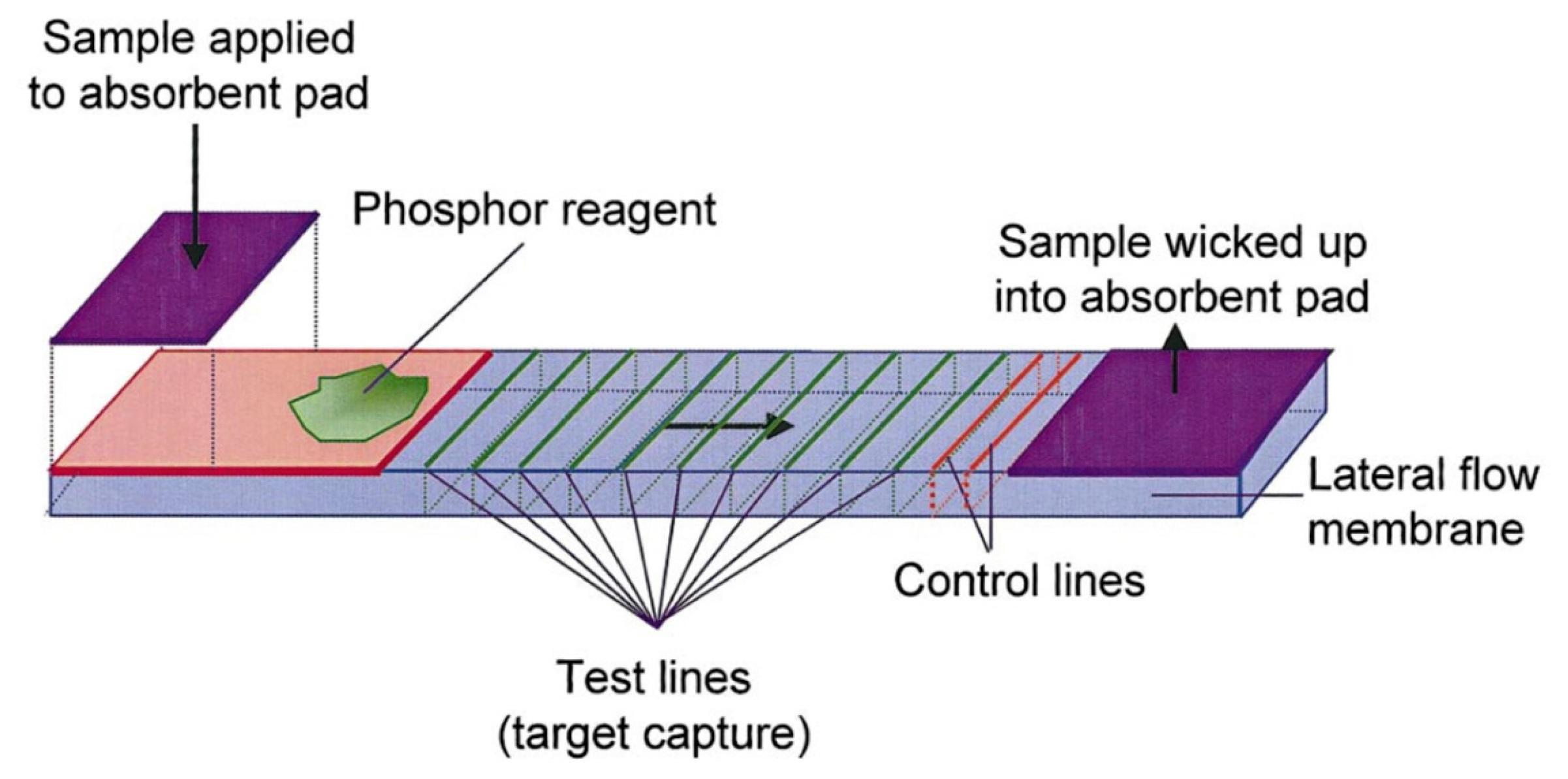
UCNPs have been used in assays for the detection of other targets, such as metal ions, toxins and metabolites [39–41]. For example, Niedbala and coworkers have demonstrated the potential of using UCNPs for the detection of different drugs of abuse, such as amphetamine, methamphetamine, phencyclidine and opiates in saliva, with 1 ng·mL−1 limit of detection [36]. In this latter study, a sandwich assay format using antibodies as biorecognition elements was used on a lateral flow test strip. The primary antibody was immobilized on the surface and the analyte was transduced using a secondary antibody labelled with UCNP. Test lines differentially provided optical signal for either the target or control, and signal intensities from test lines could be used to quantify the concentration of target in a sample, as depicted in Figure 2.
In another study for the detection of antigens, multiple targets were detected simultaneously using UCNPs with different emission profiles [42]. Aflatoxin B1 (AFB) and ochratoxin A (OTA), two types of mycotoxins, were simultaneously quantified in a competitive assay format. Using Tm3+ and Er3+ doped UCNPs decorated with anti-AFB and anti-OTA antibodies, respectively, the emission band at 452 and 660 nm were used to quantitatively identify the targets.
A further example is a system using LRET as a transduction scheme for the detection of glucose in solution [43]. In this study, UCNPs were used as the LRET donor and rhodamine B isothiocyanate (RBI) conjugated to 3-aminophenylboronic acid (APBA) was used as the acceptor. Glucose molecules were immobilized onto UCNPs. The APBA component of the RBI-APBA conjugate was then allowed to bind the glucose on the surface of UCNP, bringing the RBI into close proximity of the UCNP so that LRET would occur. When a sample solution containing glucose was added, the free glucose in solution competed for the APBA, and the RBI-APBA complex dissociated from the UCNP-glucose hindering LRET. The decrease in acceptor luminescence was used to determine the concentration of glucose in solution.
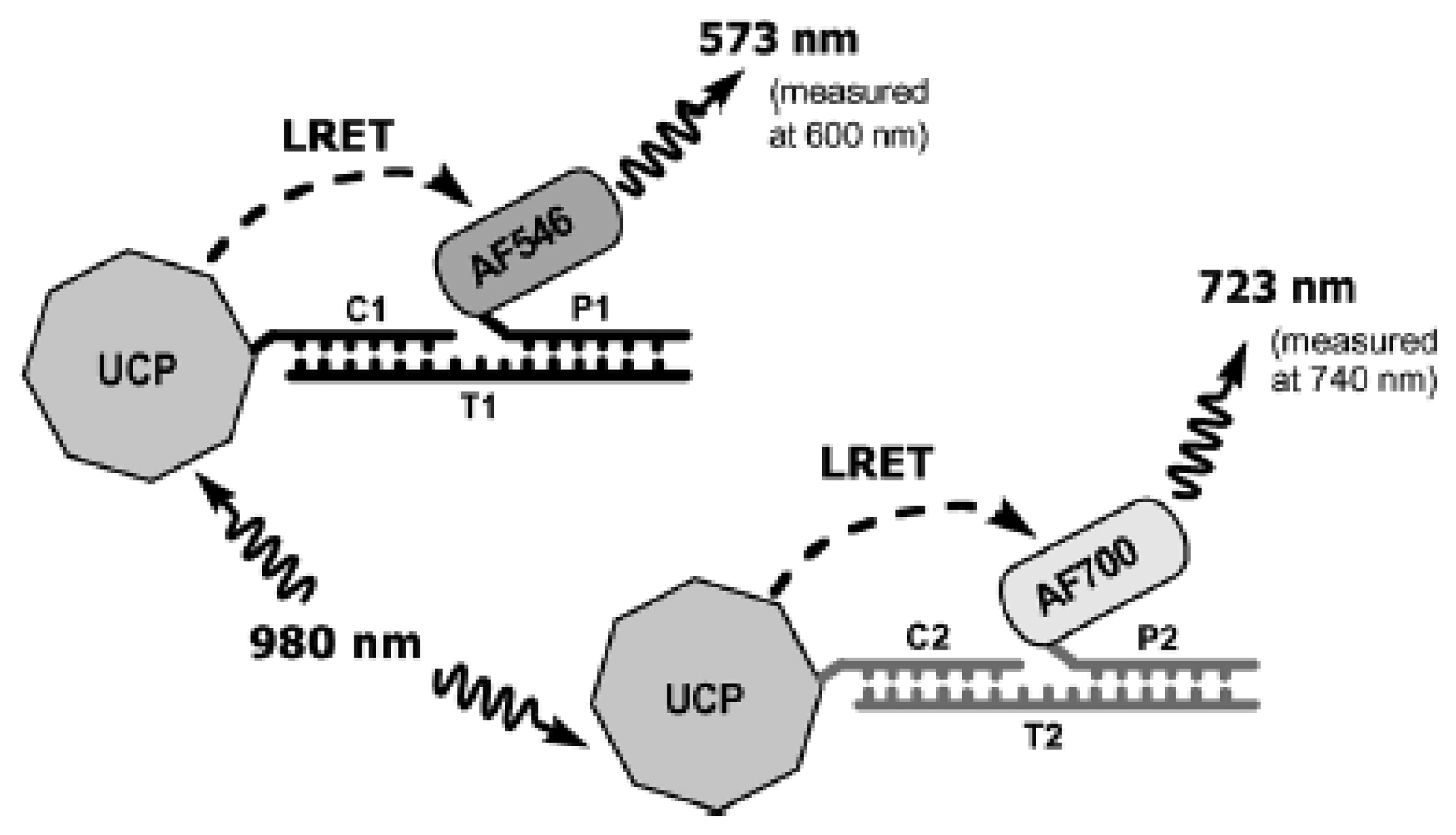
UCNPs have also been implemented extensively for DNA detection. They have been used both as direct labels and in energy transfer applications in a variety of formats, including hybridization assays and sandwich assays, both in solution and on solid supports [44–47]. One interesting example is the use of UCNP in a single donor, multiple acceptor LRET system [48]. In this study, one type of UCNP with multiple emission peaks (540 nm and 653 nm) was used as the donor for two different organic dyes, AF546 and AF700. After the UCNPs were covalently modified with the two types of capture DNA sequences, the target strands were first incubate with the dye-labeled reporter DNA before introducing the UCNP-capture DNA. After incubation, the UCNPs were excited with NIR radiation at 980 nm and emissions of the dyes were measured at 600 nm and 740 nm (Figure 3).
2.4. Time Resolved Measurements
The sensitivity and detection limit of optical bioassays that rely on emission of radiation can be limited by autofluorescence and scatter. The use of long-wavelength excitation in combination with UCNPs for bioassays has the potential to increase signal-to-background ratio and improve detection limits. The UC process associated with excitation using near-IR and IR radiation typically suffers from a low quantum yield, often being below 3% [1]. However, when such lanthanide-doped nanoparticles are excited in the UV region of the spectrum, the down conversion processes can exhibit quantum yields as high as 68% [49]. To eliminate the background signal associated with UV excitation, a pulsed excitation source is used and the emissions from lanthanides, which have lifetimes on the order of milli-seconds, are measured after the short lived background from autofluorescence and scatter has decayed in nanoseconds. The principle of time resolved luminescence (TRL) measurements is outlined in Figure 4. The use of lanthanide doped NPs in TRL has only recently been reported. However, the use of lanthanide chelates in time-resolved bioassays dates back to the mid-seventies. Lanthanide chelates have been reported for various applications such as the detection of biomolecules, visualization of live cells and analyses of metabolites [50,51].
The sensitivity of assays based on lanthanide chelates has been improved by incorporation of the chelates inside nanoparticles to increase the lanthanide-to-biomolecule ratio. For example, over 30,000 Eu(III)-2-thenoyltrifluoroacetone complexes were incorporated in 107 nm polystyrene beads, giving a 4 orders of magnitude dynamic range for the detection of PSA in levels as low as 250 zeptomoles [53]. This represents a 100-fold improvement in assay sensitivity compared to a conventional Eu-labeled streptavidin assay. However the application of such particles is limited due to their inherent large size and swelling, in addition to the leakage of the lanthanide complexes [50]. Lanthanide chelates in silica NPs represent an alternative structure and have been used in time resolved fluoroimmunoassays and time resolved luminescence imaging applications [54–56]. The use of lanthanide doped NPs such as NaYF4 [57], KGdF4 [58], CaF2 [59], ZrO2 [60], LaPO4 [49] and SiO2 [61] have been reported to offer better photostability than chelates due to the rigid crystal lattice. Lifetimes exhibited by such nanoparticles are summarized in Table 2.
The use of lanthanide doped GdF3 nanoparticles as passive labels for time resolved detection of trace amounts of avidin was reported to provide a limit of detection of 74 pM [52]. Chen et al. have reported the use of lanthanide-doped NPs in combination with UV excitation and time resolved luminescence resonance energy transfer (TR-LRET) using organic dyes as acceptors. The apparent lifetime of organic dye acceptors is increased since the long lived excited states of Ln3+ slowly populate the excited state of acceptor. This allows for the LRET signal to be free of interferences from short-lived background signals [57]. Chen's group demonstrated the first TR-LRET based assays for the detection of avidin employing biotin labeled NaYF4:Ce/Tb UCNPs and fluorescein isothiocyanate (FITC)-labeled avidin as acceptor, and reported a dynamic range spanning 4.8 nM–400 nM. The NPs were excited at 290 nm and exhibited significant emission centered at 489, 542, 585 and 623 nm. PL lifetimes based on 542 nm peak was determined to be 2.21 ms for biotinylated NPs and decreased to 0.7 ms with increasing acceptor concentration. In addition to eliminating background signals, TRL allowed for distinction between direct excitation of FITC and LRET sensitized emission based on apparent lifetimes. A similar UC-LRET methodology using Y2O2S:Er/Yb upconverting phosphors and fluorescent phycobiliprotein as acceptor demonstrated similar dynamic range 0.7–9.0 nM [62]. Other examples of TR-LRET have been reported in the literature [58–60].
Most lanthanide-based TRL assays are reported in microtitre plates and have made use of commercially available plate readers with TRL capability. Examples include implementation of SpectraMax Paradigm instruments from Molecular Devices and the Infinite m1000 system from Tecan. Time-delayed detection in plate readers is typically based on oscillator-controlled electronics. A flash lamp, laser or LED or a combination of the above is used as an excitation source and detection is facilitated by filters or monochromators. In many cases, photo multiplier tubes (PMTs) with exceptionally low dark count rates are needed for nanoparticles exhibiting low quantum yields [50].
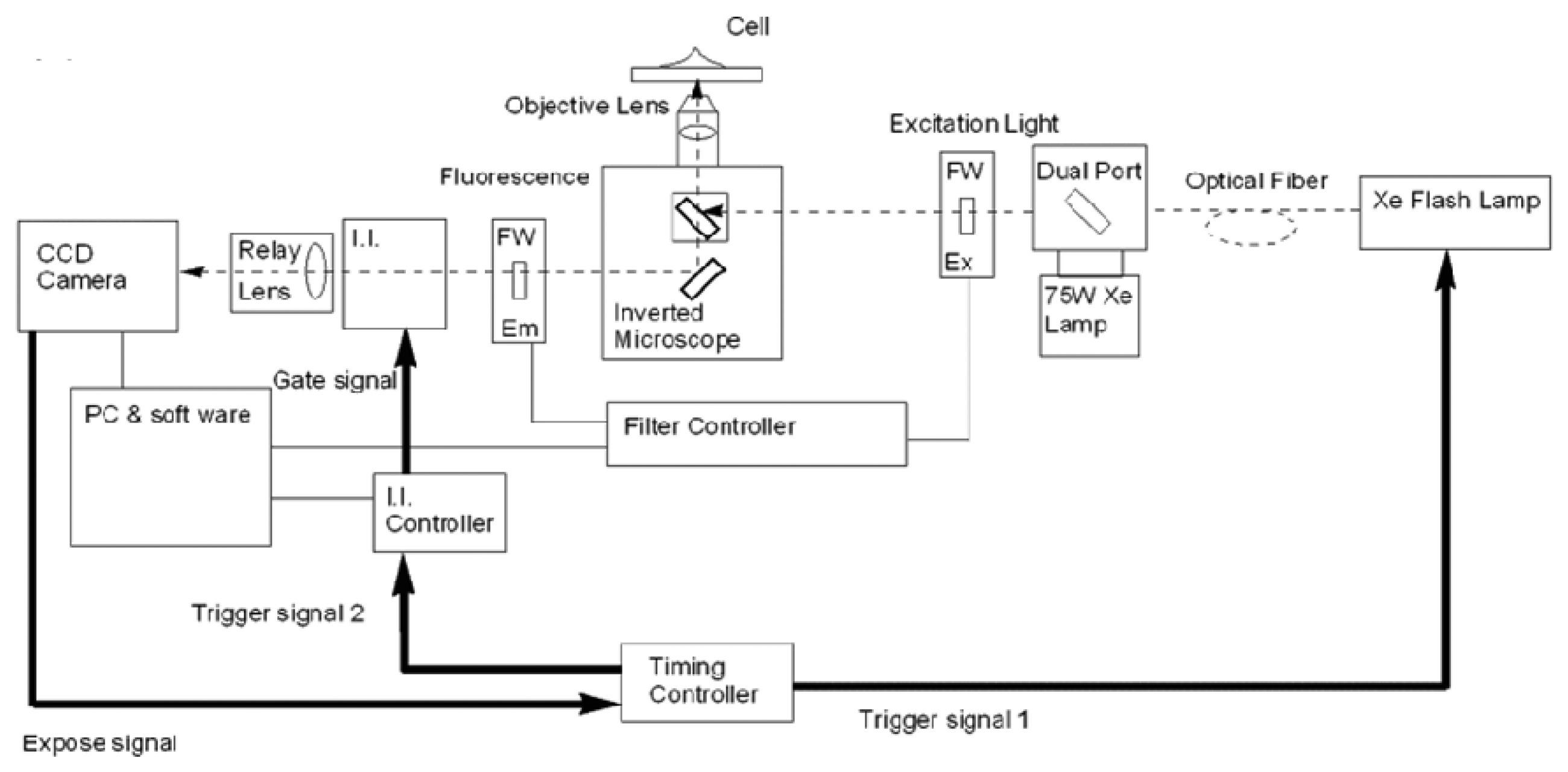
Microscopy systems for time-resolved lanthanide measurements have been reported and are often based on mechanical choppers [63–66] and can make use of image intensifier units [67,68] as a basis for achievement of time resolution. Implementation of an image intensifier facilitates control of gate and delay times and achieves better uniformity of light at the detector. Hanaoka et al. reported a time-resolved, long-lived luminescence microscopy (TRLLM) imaging system for the detection and visualization of biomolecules in live cells [69]. The schematic in Figure 5 shows the use of a xenon flash lamp as an excitation source, a time controller and an image intensifier unit. The TRLLM system was used for imaging lanthanide complexes that served as biolabels, in addition to monitoring of intracellular Zn2+ using a luminescent lanthanide-based probe.
3. CMOS Microsystem
The capability of integrating a large array of detectors with signal processing circuits, low power consumption, and low fabrication cost in high volume production are well-known features offered by the CMOS technology. In this section, three specific attributes of CMOS particularly beneficial to the integration with luminescence bioassays are examined, namely system miniaturization using contact imaging, spectral detection, and time-resolved detection.
3.1. System Miniaturization
In a conventional excitation-induced luminescence imaging system, the signal path from the excitation source to the detector often consists of bulky and expensive optical components such as a system of lenses. Contact imaging, in contrast, is a recent technique whereby the object to be imaged is placed near or directly on top of the photodetector array [70–72]. It does not require intermediary optics such as lenses, resulting in orders of magnitude improvement in sensitivity as well as significant size and cost reduction [73]. These advantages make contact imaging attractive for portable low-cost biosensor applications.
The choices of the photodetector for conventional luminescence imaging systems have been the PMT and the charge-coupled device (CCD). PMTs are amongst the most sensitive photodetectors, but are bulky, expensive and require a high operating voltage, making them unattractive to be integrated into a miniaturized system. The throughput of PMT-based detection systems is relatively low due to the lack of parallelism. CCDs can be employed in an arrayed implementation, but do not allow for the on-silicon-chip integration of peripheral circuits such as signal conditioning circuits. This increases cost and limits miniaturization. CMOS technology, on the other hand, has the advantages of low cost, high integration density, and signal processing versatility. Numerous recent designs based on the CMOS p-n-junction photodiode have been reported for many bioluminescence detection lab-on-chip devices [74–78]. The monochromatic photogate structure typically used in a CCD has been demonstrated in CMOS. However, the exploitation of the CMOS polysilicon photogate to perform spectral sensing has largely been unexplored.
To illustrate key concepts of miniaturization by combining contact imaging and CMOS spectral detection, key design concepts of a CMOS fluorescence analysis microsystem [79] is discussed. The microsystem integrates a high-performance optical interference filter and a 128 × 128 pixel active pixel sensor fabricated in a standard 0.35 μm CMOS technology. The thin-film filter has an optical density greater than 6.0 at the wavelength of interest, providing ample excitation rejection to the 532 nm solid-state laser. Microsystem performance is experimentally validated by imaging spots of the Cyanine-3 fluorophore, conventionally used in DNA detection. Detection limit was measured to be 5000 fluorophores/μm2.
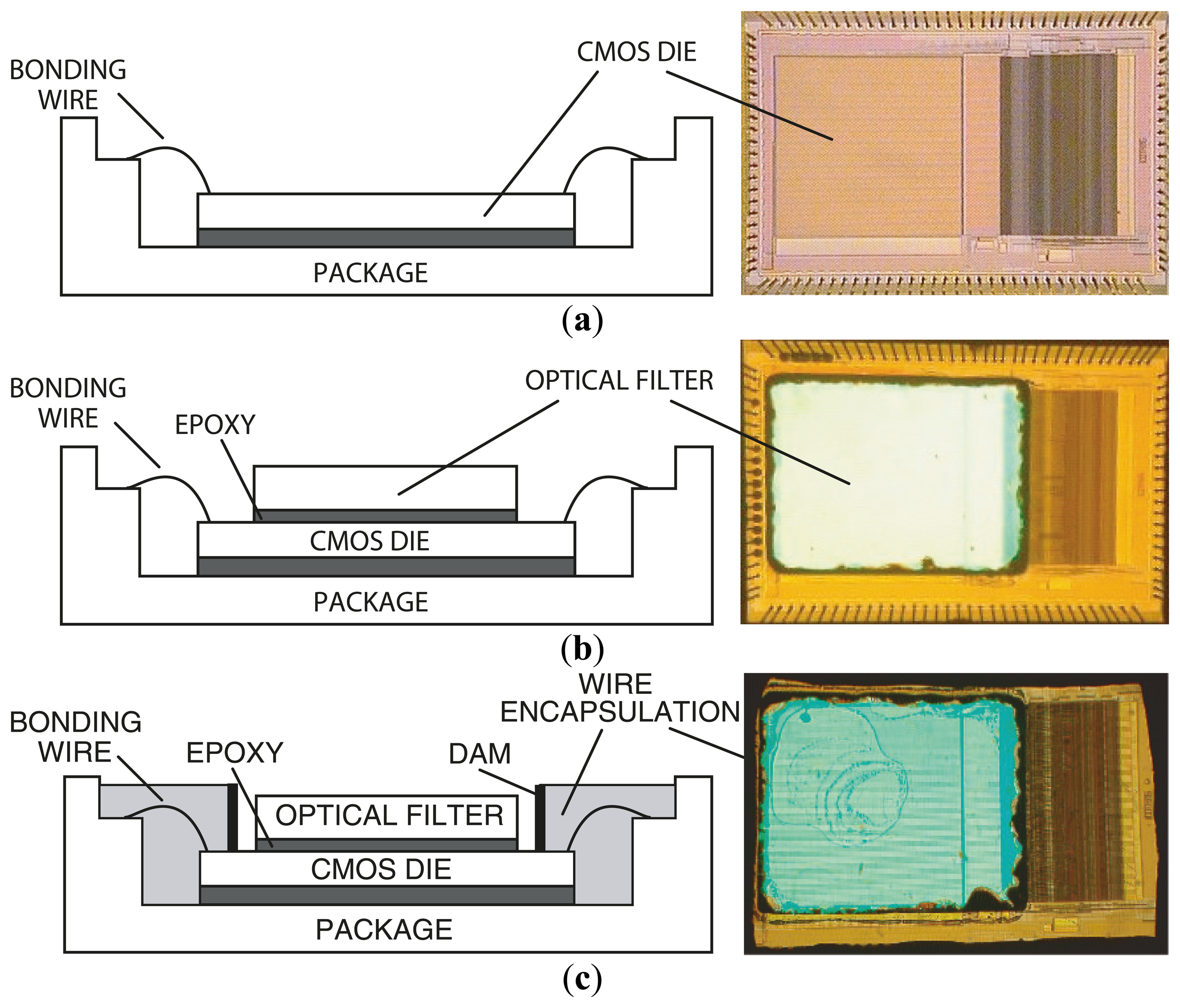
Figure 6 describes the steps in microsystem integration. Figure 6a shows the CMOS die bonded and packaged using a standard wire bonding and packaging process. The CMOS die was raised inside the chip package by placing a die spacer below it. This brings the CMOS photo detector array closer to the top surface of the chip package, where the sample is placed. Figure 6b shows the attachment of the optical filter to the CMOS die using a refractive-index-matched epoxy, which eliminates unwanted light reflections at the filter–CMOS die surface. Finally, as depicted in Figure 6c, an opaque epoxy dam is built around the optical filter. Then, an epoxy is poured over the bonding wires. This bonding wire encapsulation electrically insulates the bonding wires, protects them, and prevents stray reflected laser light from leaking through the sides of the filter thus reaching the sensor array.
The optical filter chosen for the microsystem is a discrete thin-film interference filter, which was designed, fabricated (Omega Optical), and optically tested prior to integration with the CMOS die. This also makes the system more flexible in serving a wide variety of applications. To adapt the system for UCNP bioassays, the 570 nm long pass filter can be readily replaced with a 900 nm short pass filter to suit the NIR excitation of UCNPs. An alternative to post-fabrication filter attachment is direct deposition. However, direct thin-film deposition over the CMOS die leads to higher complexity due to complications in adjusting the fabrication process to compensate for the temperature and material differences between the surface of the optical filter and the CMOS die. The masking of bonding pads during the coating process in the direct deposition method also adds additional complexity. In the presented approach, a 100 μm-thick 25 mm × 25 mm optical filter is diced into smaller pieces of size 2.2 mm × 2.8 mm each (by diamond saw, performed at Corwil). The small-sized filter is then attached to the CMOS die. The interference filter was fabricated using 60 layers of Nb2O5 and SiO2. The coatings were deposited onto a 100 μm-thick microsheet of fused silica substrate by physical vapor deposition.
3.2. CMOS Spectral Detection
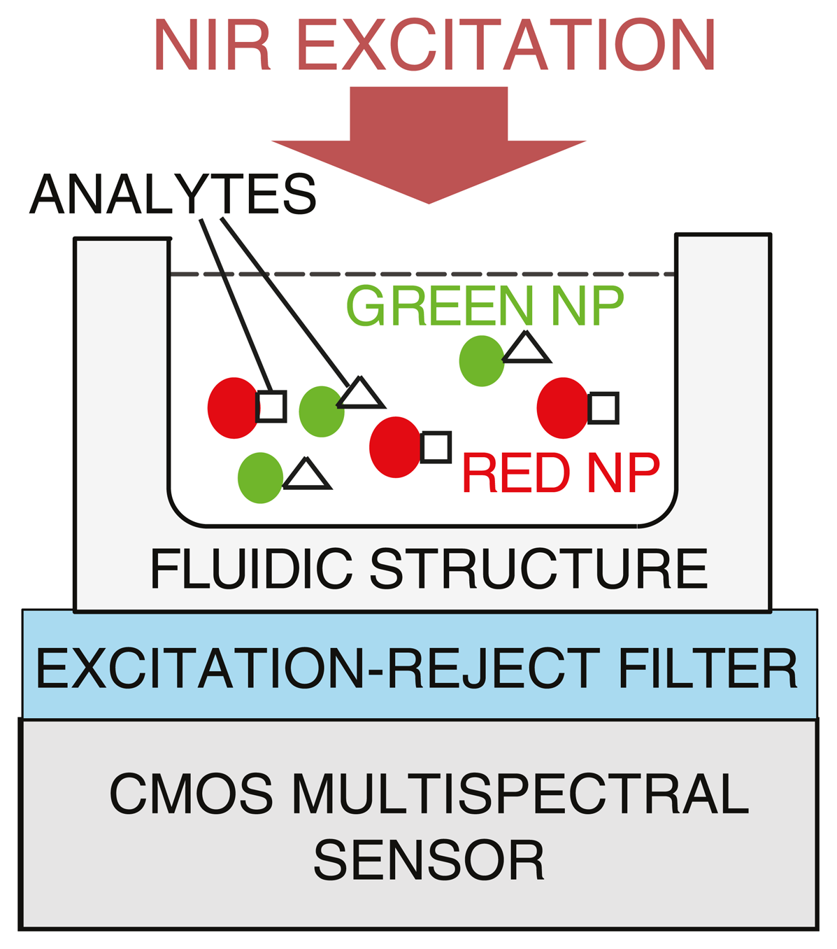
Optical tuning of emission wavelengths for UCNPs enables unprecedented flexibility in spectral multiplexing. For example in DNA detection, different DNA target sequences can be tagged with labels that emit light at different wavelengths, which can be concurrently detected and distinguished. Unlike other spectroscopic techniques, such as Raman spectroscopy, where continuous fine spectral resolution is required, luminescence imaging requires spectral differentiation among only a few discrete wavelengths, typically well-separated (i.e., <50 nm apart) in the visible band [70]. To avoid the complexity and variability associated with surface chemistry common to spatially multiplexed arrays such as microarrays, spectrally-multiplexed assays using UCNPs can be developed, as depicted in Figure 7.
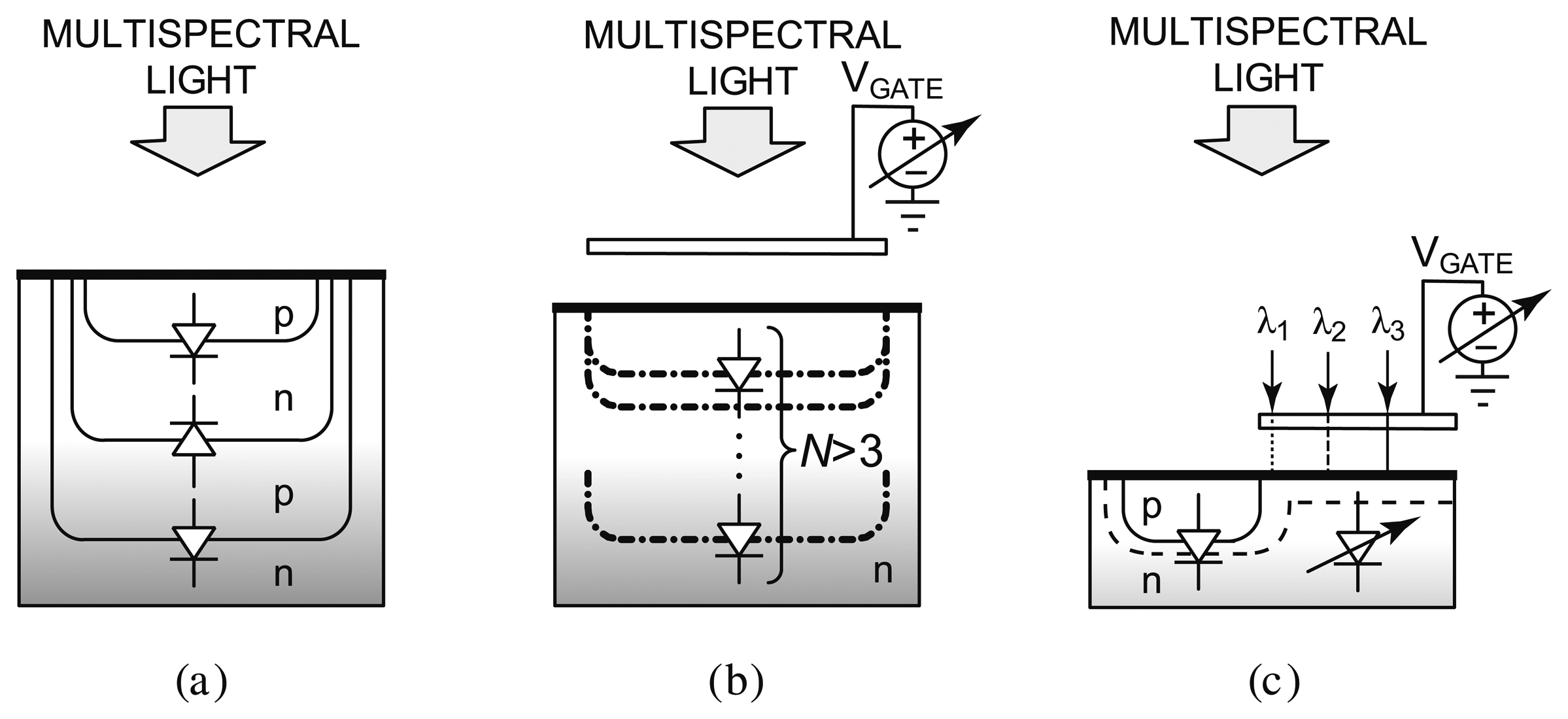
Recently, CMOS technology has been researched for integrated spectral detection. Requiring a reduced amount of external optical components or none at all, these CMOS systems enable a new breed of compact, low-cost luminescence detection systems. Figure 8 illustrates the evolution of CMOS filterless spectral sensing approaches. Conventionally, differentiation between luminescence emission wavelengths has been achieved by using a set of optical bandpass filters to select different parts of the emission spectrum. The optics involved is bulky and expensive. To circumvent this problem, other spectral methods have also been investigated. Methods based on diffraction grating (the splitting of light) [80] and Fabry-Perot etalon (tuned resonance cavity) [81] generally offer high spectral resolution, but require micromachining and post-processing such as wafer polishing and wafer bonding. Eliminating the need for sophisticated optics and post-processing is the ultimate remedy to the high design complexity and fabrication cost.
Techniques that solely rely on integrated circuit process technology have been developed, most notably buried junction technology [82,84–86], on which the Foveon sensor [87] is based, as shown in Figure 8a. Since light absorption in a semiconductor varies across wavelengths in such a way that light of a longer wavelength can penetrate deeper, a photocurrent measured at a deeper depth consists of stronger long wavelength components. By sensing at several depths, color information can be inferred. Although the buried junction approach achieves high spatial density and is suitable for photographic applications requiring only three colors (e.g., blue, green, and red), there is a limit to the number of diodes that can be implemented into a vertical stack, for example three for a dual-well process. This renders it unsuitable for applications that require sensing more than three wavelengths. To overcome this limitation, a spectrally-sensitive photodiode that can potentially sense more than three colors has been developed [83], as shown in Figure 8b. A biased poly-silicon gate modulates the photo sensing region depth to effectively achieve an equivalence of many buried p-n-junctions. However, the reliance on the vertical dimensions of the CMOS process technology limits the scalability of the device dimensions. The most recently reported prototype is fabricated in a 5 μm custom process [88].
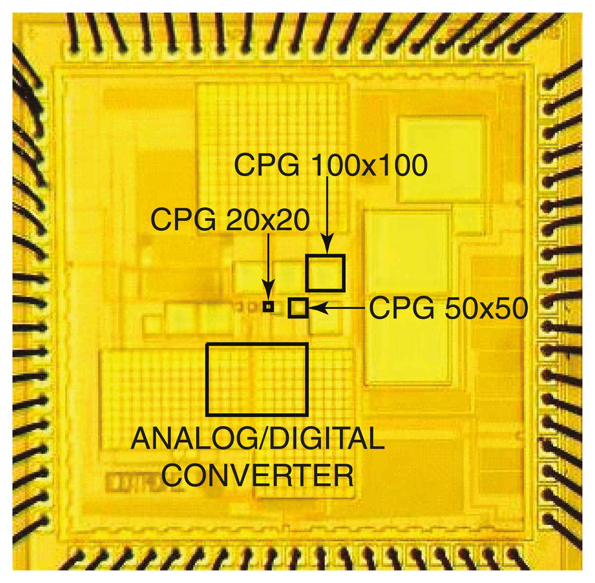
Figure 8c depicts a new approach that employs a voltage to tune the spectral response of a detector [89–91]. Sensing of a small set of well separated wavelengths (e.g., >50 nm apart) is achieved by tuning the spectral response of the device with a bias voltage. Termed the CMOS photogate (CPG), it employs the polysilicon gate as an optical filter, which eliminates the need for an external color filter. Multiple measurements with different color components are collected. A back-end algorithm then solves the inverse problem by computing the different color intensity components from prior knowledge of the dependency of detector response to voltage. A prototype has been fabricated in a standard 0.35 μm digital CMOS technology, depicted in Figure 9. It demonstrates intensity measurements of blue (450 nm), green (520 nm), and red (620 nm) illumination with a peak signal-to-noise ratio (SNR) of 34.7 dB, 29.2 dB, and 34.8 dB, respectively. The prototype has been applied to detect green-emitting quantum dots (gQDs) and red-emitting quantum dots (rQDs). It spectrally differentiated among multiple emission bands, effectively implementing on-chip emission filtering. The prototype demonstrated single-color measurements of gQD and rQD concentrations to a detection limit of 24 nM, and multi-color measurements of solutions containing both colors of QDs to a detection limit of 90 nM and 120 nM of gQD and rQD, respectively.
To illustrate the application of spectral multiplexing in DNA analysis, a fluorescence contact imaging microsystem [92] is described below. The microsystem integrates a filterless CMOS CPG sensor that exploits the polysilicon gate as an optical filter. The CPG is applied to fluorescence-based transduction in a spectrally multiplexed format by differentiating among multiple emission bands, hence replacing the functionality of a bank of emission filters. The CPG was fabricated in a standard 0.35 μm CMOS technology. The multi-color imaging capability of the microsystem in analyzing DNA targets has been validated in the detection of marker gene sequences for the spinal muscular atropy disease and the E. coli bacteria. Spectral-multiplexing enabled the two DNA targets to be simultaneously detected with a measured detection limit of 240 nM and 210 nM for the two target concentrations at a sample volume of 10 μL for the green and red transduction channels, respectively.
3.3. CMOS Time-Resolved Measurement
Similar to conventional fluorophores or quantum dots, UCNPs can also be used in time-resolved measurements. Time-resolved imaging is a technique where low-light signals are recorded with high timing resolution relative to a synchronized optical impulse excitation, in order to extract the characteristic luminescence decay constant or lifetime [93]. For example in time-correlated single photon counting (TCSPC), a typical apparatus includes a pulsed optical source, a discrete detector such as an avalanche photodiode (APD) or PMT, external time-to-digital converter (TDC) and a workstation to compute the decay constant, resulting in a bulky, expensive and power-hungry acquisition system. A major limitation of this approach is the restrictively low photon count limit that is below 5% of the excitation rate, which is necessary to avoid distortion due to photon pile-up caused by both long detector dead-time and the inability of the TDC to process more than one event per excitation period. Therefore, TCSPC has in the past been limited by peak acquisition rates of around 1 MHz [94].
Recent advances in single-photon avalanche diodes (SPADs) and on-chip TDCs implemented in standard CMOS processes have enabled TCSPC measurements to be performed by an imaging array, and with much higher time resolution [94]. To assess the state-of-the-art in CMOS integrated systems for time-resolved imaging, several recently reported prototypes with their features and implementation approaches are summarized next.
A CMOS image sensor with direct digital phase output is reported in [95]. A row-level zero-crossing detection is implemented to extract the phase-shift between the intensity modulated excitation signal and the emitted fluorescence, generating a time delay signal proportional to the fluorescence lifetime of the target analyte. A time-interpolated TDC is subsequently used to quantize the time delay into a digital representation of the phase-shift for post-signal processing and image reconstruction. The design has been implemented in a low-power 65 nm CMOS technology. The TDC features a temporal resolution of 110 ps over a 414 s range, which corresponds to a dynamic range of 132 dB. Extensive characterization results demonstrate a phase readout sensitivity of better than 0.01 degrees at a 1.2 kHz modulation frequency and 0.1 degrees at up to 1 MHz. This design is an example of the high-precision time-domain processing capability CMOS technology can achieve.
Much engineering has gone into improving the optical signal handling capability of the CMOS technologies. In [96], a time-resolved CMOS image sensor with draining-only modulation (DOM) pixels for time-domain fluorescence lifetime imaging is reported. In the DOM pixel, which uses the pinned photodiode (PPD) technology, a time-windowed signal charge transfer from a PPD to a pinned storage diode (PSD) is controlled by a draining gate only, without a transfer gate between the two diodes. This structure allows potential barrierless and trapless charge transfer from the PPD to the PSD. A 256 × 256 pixel time-resolved CMOS imager with 7.5 × 7.5 μm2 DOM pixels has been implemented using 0.18 μm CMOS image sensor process technology with PPD option. The prototype demonstrated high sensitivity for weak signal of less than one electron per light pulse, and accurate measurement of fluorescence decay with subnanosecond time resolution.
A CMOS imager with column-level 10-bit TDC array for time-resolved optical sensing is reported in [97]. This imager is one of the first fully integrated system for photon time-of-arrival evaluation. The sensor comprises an array of 128 × 128 single-photon pixels, a bank of 32 TDCs, and a 7.68 Gbps readout system. Outstanding timing precision of single-photon avalanche diodes and the optimized measurement circuitry enable a resolution of 97 ps within a range of 100 ns. Accurate measurements are achieved based on a short integration time of 50 ms even when signal photon count rates as low as a few hundred photons per second. Aside from fast fluorescence lifetime imaging, the system is also suitable for applications include 3-D imaging (i.e., distance measurement), optical range finding and, more generally, imaging based on time-correlated single photon counting.
A CMOS image sensor with in-pixel two-stage charge transfer for time-resolved fluorescence lifetime imaging with sub-nanosecond time resolution is presented in [98]. In order to analyze the fluorescence lifetime, the proposed CMOS image sensor has two charge transfer stages using a pinned photodiode structure in which the first charge transfer stage is for the time-resolved sifting of fluorescence in all the pixels simultaneously and the second charge transfer stage is for reading the signals in each pixel sequentially with correlated double sampling operation. A 0.18 μm CMOS image sensor technology with a pinned photodiode process option is used for the implementation of a 256 × 256 pixel CMOS image sensor. The decaying images and lifetimes of fura-2 solutions having different concentrations have been measured with a 250 ps time step using an ultraviolet laser diode as a light source.
A fully digital single-chip solution to fluorescence lifetime sensing implementing lifetime estimation on-chip using the centre-of-mass method (CMM) is presented in [94]. The device comprises a 1.3 × 1.7 mm2 CMOS chip in 0.13 μm technology, featuring an array of SPAD detectors in a silicon photomultiplier architecture, the multichannel TDC architecture, a CMM processing block and a serial interface for control and data capture. This design provides mitigation to the pulse pile-up problem. A time-multiplexed, multichannel TDC architecture is introduced to allow the pile-up limit to be broken, achieving a maximum 100 Mphoton/s acquisition rate, allowing lifetime decays of common organic fluorophores to be obtained.
A miniaturized, high-throughput, time-resolved fluorescence lifetime sensor implemented in a 0.13 μm CMOS process is described in [99]. The design combines single photon detection, multiple channel timing and embedded pre-processing of fluorescence lifetime estimations on a single device. Detection is achieved using an array of SPADs arranged in a digital silicon photomultiplier architecture with 400 ps output pulses and a 10% fill-factor. An array of TDCs with 50 ps resolution records up to 8 photon events during each excitation period. Data from the TDC array is then processed using the CMM method to produce fluorescence lifetime estimations in real-time. The system was demonstrated in a practical laboratory environment with measurements of a variety of fluorescent dyes with different single exponential lifetimes, showing the ability of the sensor to overcome the classic pile-up limitation of TCSPC by over an order of magnitude.
A two-chip micro-scale time-resolved fluorescence analyzer integrating excitation, detection, and filtering is described in [100]. This design achieves a new level of system integration. A new 8 × 8 array of drivers realized in standard low-voltage 0.35 μm CMOS is bump-bonded to AlInGaN blue micro-pixellated light-emitting diodes (micro-LEDs). The array is capable of producing sample excitation pulses with a width of 777 ps (FWHM), enabling short lifetime fluorophores to be investigated. The fluorescence emission is detected by a second, vertically-opposed 16 × 4 array of SPADs fabricated in 0.35 μm high-voltage CMOS technology with in-pixel time-gated photon counting circuitry. Captured chip data are transferred to a personal computer for further processing, including histogram generation, lifetime extraction, calibration and background/noise compensation. The system was demonstrated with measurements of fluorescent colloidal quantum dot and Rhodamine samples.
A SPAD–based pixel array for the analysis of fluorescence phenomena is presented in [101]. Each 150 × 150 μm2 pixel integrates a single photon detector combined with an active quenching circuit and a 17-bit digital events counter. On-chip master logic provides the digital control phases required by the pixel array with a full programmability of the main timing synchronisms. The pixel exhibits an average dark count rate of 3 kcps and a dynamic range of over 120 dB in time uncorrelated operation. Time-resolved fluorescence measurements have been demonstrated by detecting the fluorescence decay of quantum-dot samples without the aid of any optical filters for excitation laser light cutoff.
An integrated CMOS sensor array for fluorescence applications which enables time-gated, time-resolved fluorescence spectroscopy is presented in [102]. The 64 × 64 array is sensitive to photon densities as low as 8.8 × 10⁶ photons/cm2 with 64-point averaging. Through a differential pixel design, the prototype has a measured impulse response of 800 ps.
The design and characterization of a low-noise time-resolved image sensor fabricated in a 130 nm CMOS process is reported in [103]. Each pixel within the 32 × 32 pixel array contains a low-noise single-photon detector and a high-precision TDC. The 10-bit TDC exhibits a timing resolution of 119 ps with a timing uniformity across the entire array of less than two least significant bits (LSBs). The differential non-linearity (DNL) and integral non-linearity (INL) are at ±0.4 and ±1.2 LSBs, respectively. The pixel array was fabricated with a pitch of 50 μm in both directions and with a total TDC area of less than 2000 μm2. The target application for this sensor is time-resolved imaging, in particular fluorescence lifetime imaging microscopy.
A 32 × 32 pixel image sensor with analog counting pixels for time-gated fluorescence lifetime detection based on SPADs is reported in [104]. The sensor, fabricated in a high-voltage 0.35 μm CMOS technology, uses an analog counting approach to minimize the area occupation of pixel electronics while maintaining a nanosecond timing resolution and shotnoise-limited operation. The all n-type field-effect transistor (nFET) pixel is formed by 12 transistors and features 25-μm pitch, achieving a 20.8% fill factor. The chip includes a phase-locked loop circuit for gating window generation, working at a maximum repetition frequency of 40 MHz. The sensor can be gated at frequency up to 80 MHz using an external delay generator. Optical characterization with a picosecond-pulsed laser showed a minimum gating window width of 1.1 ns.
4. Conclusions
Two characteristics are noteworthy when combining the use of UCNP with CMOS technology. First, the excitation for UCNPs is in the near-infrared band. Due to the bandgap of silicon, typical CMOS detectors have a quantum efficient of below 10% for wavelengths longer than 900 nm. Therefore, since silicon is a poor absorber of the NIR excitation, using CMOS with UCNP reduces the excitation-rejection optical filter attenuation requirement.
Second, for time-resolved measurements, the UCNPs can operate in luminescence at the micro-second time frame, which is much longer than that of fluorescence with a lifetime typically in the nano-second time frame. While modern CMOS technology is capable of operating on the nano-second time scale, operating CMOS circuits at high speeds leads to high power consumption. High-speed operation can be achieved with acceptable power consumption with the use of modern, highly scaled CMOS processes. However, this leads to high fabrication cost and is especially not suitable for the low-volume analytical instrumentation market (as opposed to high-volume consumer electronics). Therefore, in this respect, employing UCNPs with CMOS offer substantial power advantage, which translates to reduced system complexity and cost.
The synergy between UCNPs and CMOS is currently a new concept. As a result, experimental prototypes are not widely demonstrated. By highlighting key characteristics and advantages, this paper is intended to stimulate further research in this emerging area.
Conflicts of Interest
The authors declare no conflict of interest.
References
- DaCosta, M.V.; Doughan, S.; Han, Y.; Krull, U.J. Lanthanide upconversion nanoparticles and applications in bioassays and bioimaging: A review. Anal. Chim. Acta 2014, 832, 1–33. [Google Scholar]
- Auzel, F. Upconversion and anti-stokes processes with f and d ions in solids. Chem. Rev. 2003, 104, 139–174. [Google Scholar]
- Chen, G.; Qiu, H.; Prasad, P.N.; Chen, X. Upconversion nanoparticles: Design, nanochemistry, and applications in theranostics. Chem. Rev. 2014, 114, 5161–5214. [Google Scholar]
- Heer, S.; Kömpe, K.; Güdel, H.U.; Haase, M. Highly efficient multicolour upconversion emission in transparent colloids of lanthanide-doped NaYF4 nanocrystals. Adv. Mater. 2004, 16, 2102–2105. [Google Scholar]
- Wang, F.; Liu, X. Upconversion multicolor fine-tuning: Visible to near-infrared emission from lanthanide-doped NaYF4 nanoparticles. J. Am. Chem. Soc. 2008, 130, 5642–5643. [Google Scholar]
- Ostermayer, F.W.; van Uitert, L.G. Cooperative energy transfer from Yb3+ to Tb3+ in YF3. Phys. Rev. B 1970, 1, 4208–4212. [Google Scholar]
- Wang, M.; Liu, J.-L.; Zhang, Y.-X.; Hou, W.; Wu, X.-L.; Xu, S.-K. Two-phase solvothermal synthesis of rare-earth doped NaYF4 upconversion fluorescent nanocrystals. Mater. Lett. 2009, 63, 325–327. [Google Scholar]
- Li, Z.; Zhang, Y.; Jiang, S. Multicolor core/shell-structured upconversion fluorescent nanoparticles. Adv. Mater. 2008, 20, 4765–4769. [Google Scholar]
- Zhang, H.; Li, Y.; Lin, Y.; Huang, Y.; Duan, X. Composition tuning the upconversion emission in NaYF4:Yb/Tm hexaplate nanocrystals. Nanoscale 2011, 3, 963–966. [Google Scholar]
- Ren, G.; Zeng, S.; Hao, J. Tunable multicolor upconversion emissions and paramagnetic property of monodispersed bifunctional lanthanide-doped NaGdF4 nanorods. J. Phys. Chem. C 2011, 115, 20141–20147. [Google Scholar]
- Chen, G.; Qiu, H.; Fan, R.; Hao, S.; Tan, S.; Yang, C.; Han, G. Lanthanide-doped ultrasmall yttrium fluoride nanoparticles with enhanced multicolor upconversion photoluminescence. J. Mater. Chem. 2012, 22, 20190–20196. [Google Scholar]
- Wang, J.; Wang, F.; Xu, J.; Wang, Y.; Liu, Y.; Chen, X.; Chen, H.; Liu, X. Lanthanide-doped LiYF4 nanoparticles: Synthesis and multicolor upconversion tuning. Comptes Rendus Chim. 2010, 13, 731–736. [Google Scholar]
- Vetrone, F.; Boyer, J.C.; Capobianco, J.A.; Speghini, A.; Bettinelli, M. Significance of Yb3+ concentration on the upconversion mechanisms in codoped Y2O3:Er3+, Yb3+ nanocrystals. J. Appl. Phys. 2004, 96, 661–667. [Google Scholar]
- Chen, G.; Liu, H.; Somesfalean, G.; Liang, H.; Zhang, Z. Upconversion emission tuning from green to red in Yb3+/Ho3+-codoped NaYF4 nanocrystals by tridoping with Ce3+ ions. Nanotechnology 2009. [Google Scholar] [CrossRef]
- Li, H.; Wang, J.; Nan, F.; Liang, S.; Zhong, Y.; Zhou, L.; Wang, Q. Upconversion luminescence properties of Mn2+-doped NaYF4:Yb/Er nanoparticles. Wuhan Univ. J. Nat. Sci. 2013, 18, 207–212. [Google Scholar]
- Qian, H.-S.; Zhang, Y. Synthesis of hexagonal-phase core−shell NaYF4 nanocrystals with tunable upconversion fluorescence. Langmuir 2008, 24, 12123–12125. [Google Scholar]
- Wang, F.; Deng, R.; Wang, J.; Wang, Q.; Han, Y.; Zhu, H.; Chen, X.; Liu, X. Tuning upconversion through energy migration in core-shell nanoparticles. Nat. Mater. 2011, 10, 968–973. [Google Scholar]
- Gorris, H.H.; Ali, R.; Saleh, S.M.; Wolfbeis, O.S. Tuning the dual emission of photon-upconverting nanoparticles for ratiometric multiplexed encoding. Adv. Mater. 2011, 23, 1652–1655. [Google Scholar]
- Bednarkiewicz, A.; Nyk, M.; Samoc, M.; Strek, W. Up-conversion fret from Er3+/Yb3+:NaYF4 nanophosphor to cdse quantum dots. J. Phys. Chem. C 2010, 114, 17535–17541. [Google Scholar]
- Dou, Q.; Zhang, Y. Tuning of the structure and emission spectra of upconversion nanocrystals by alkali ion doping. Langmuir 2011, 27, 13236–13241. [Google Scholar]
- Nguyen, T.L.; Spizzirri, P.; Wilson, G.; Mulvaney, P. Tunable light emission using quantum dot-coated upconverters. Chem. Commun. 2008. [Google Scholar] [CrossRef]
- Wang, L.; Yan, R.; Huo, Z.; Wang, L.; Zeng, J.; Bao, J.; Wang, X.; Peng, Q.; Li, Y. Fluorescence resonant energy transfer biosensor based on upconversion-luminescent nanoparticles. Angew. Chem. Int. Ed. 2005, 44, 6054–6057. [Google Scholar]
- Haase, M.; Schäfer, H. Upconverting nanoparticles. Angew. Chem. Int. Ed. 2011, 50, 5808–5829. [Google Scholar]
- Saboktakin, M.; Ye, X.; Oh, S.J.; Hong, S.H.; Fafarman, A.T.; Chettiar, U.K.; Engheta, N.; Murray, C.B.; Kagan, C.R. Metal-enhanced upconversion luminescence tunable through metal nanoparticle-nanophosphor separation. ACS Nano 2012, 6, 8758–8766. [Google Scholar]
- Schietinger, S.; Aichele, T.; Wang, H.Q.; Nann, T.; Benson, O. Plasmon-enhanced upconversion in single NaYF4:Yb3+/Er3+ codoped nanocrystals. Nano Lett. 2010, 10, 134–138. [Google Scholar]
- Feng, W.; Sun, L.D.; Yan, C.H. Ag nanowires enhanced upconversion emission of NaYF4:Yb,Er nanocrystals via a direct assembly method. Chem. Commun. 2009. [Google Scholar] [CrossRef]
- Zhang, H.; Li, Y.; Ivanov, I.A.; Qu, Y.; Huang, Y.; Duan, X. Plasmonic modulation of the upconversion fluorescence in NaYF4:Yb/Tm hexaplate nanocrystals using gold nanoparticles or nanoshells. Angew. Chem. Int. Ed. 2010, 49, 2865–2868. [Google Scholar]
- Li, Z.Q.; Li, X.D.; Liu, Q.Q.; Chen, X.H.; Sun, Z.; Liu, C.; Ye, X.J.; Huang, S.M. Core/shell structured NaYF4:Yb3+/Er3+/Gd3+ nanorods with au nanoparticles or shells for flexible amorphous silicon solar cells. Nanotechnology 2012. [Google Scholar] [CrossRef]
- Liu, N.; Qin, W.; Qin, G.; Jiang, T.; Zhao, D. Highly plasmon-enhanced upconversion emissions from Au@β-NaYF4:Yb,Tm hybrid nanostructures. Chem. Commun. 2011, 47, 7671–7673. [Google Scholar]
- Zhao, P.; Zhu, Y.; Yang, X.; Fan, K.; Shen, J.; Li, C. Facile synthesis of upconversion luminescent mesoporous Y2O3:Er microspheres and metal enhancement using gold nanoparticles. RSC Adv. 2012, 2, 10592–10597. [Google Scholar]
- Zhang, W.; Ding, F.; Chou, S.Y. Large enhancement of upconversion luminescence of NaYF4:Yb3+/Er3+ nanocrystal by 3d plasmonic nano-antennas. Adv. Mater. 2012, 24, OP236–OP241. [Google Scholar]
- Rosenblum, L.T.; Kosaka, N.; Mitsunaga, M.; Choyke, P.L.; Kobayashi, H. In vivo molecular imaging using nanomaterials: General in vivo characteristics of nano-sized reagents and applications for cancer diagnosis. Mol. Membr. Biol. 2010, 27, 274–285. [Google Scholar]
- Cheng, L.; Wang, C.; Liu, Z. Upconversion nanoparticles and their composite nanostructures for biomedical imaging and cancer therapy. Nanoscale 2013, 5, 23–37. [Google Scholar]
- Zijlmans, H.J.M.A.A.; Bonnet, J.; Burton, J.; Kardos, K.; Vail, T.; Niedbala, R.S.; Tanke, H.J. Detection of cell and tissue surface antigens using up-converting phosphors: A new reporter technology. Anal. Biochem. 1999, 267, 30–36. [Google Scholar]
- Hampl, J.; Hall, M.; Mufti, N.A.; Yao, Y.M.M.; MacQueen, D.B.; Wright, W.H.; Cooper, D.E. Upconverting phosphor reporters in immunochromatographic assays. Anal. Biochem. 2001, 288, 176–187. [Google Scholar]
- Niedbala, R.S.; Feindt, H.; Kardos, K.; Vail, T.; Burton, J.; Bielska, B.; Li, S.; Milunic, D.; Bourdelle, P.; Vallejo, R. Detection of analytes by immunoassay using up-converting phosphor technology. Anal. Biochem. 2001, 293, 22–30. [Google Scholar]
- Zuiderwijk, M.; Tanke, H.J.; Niedbala, R.S.; Corstjens, P.L.A.M. An amplification-free hybridization-based DNA assay to detect streptococcus pneumoniae utilizing the up-converting phosphor technology. Clin. Biochem. 2003, 36, 401–403. [Google Scholar]
- Yan, Z.; Zhou, L.; Zhao, Y.; Wang, J.; Huang, L.; Hu, K.; Liu, H.; Wang, H.; Guo, Z.; Song, Y.; et al. Rapid quantitative detection of yersinia pestis by lateral-flow immunoassay and up-converting phosphor technology-based biosensor. Sens. Actuators B Chem. 2006, 119, 656–663. [Google Scholar]
- Kuningas, K.; Ukonaho, T.; Päkkilä, H.; Rantanen, T.; Rosenberg, J.; Lövgren, T.; Soukka, T. Upconversion fluorescence resonance energy transfer in a homogeneous immunoassay for estradiol. Anal. Chem. 2006, 78, 4690–4696. [Google Scholar]
- Wu, S.; Duan, N.; Wang, Z.; Wang, H. Aptamer-functionalized magnetic nanoparticle-based bioassay for the detection of ochratoxin a using upconversion nanoparticles as labels. Analyst 2011, 136, 2306–2314. [Google Scholar]
- Päkkilä, H.; Ylihärsilä, M.; Lahtinen, S.; Hattara, L.; Salminen, N.; Arppe, R.; Lastusaari, M.; Saviranta, P.; Soukka, T. Quantitative multianalyte microarray immunoassay utilizing upconverting phosphor technology. Anal. Chem. 2012, 84, 8628–8634. [Google Scholar]
- Wu, S.; Duan, N.; Zhu, C.; Ma, X.; Wang, M.; Wang, Z. Magnetic nanobead-based immunoassay for the simultaneous detection of aflatoxin b1 and ochratoxin a using upconversion nanoparticles as multicolor labels. Biosens. Bioelectron. 2011, 30, 35–42. [Google Scholar]
- Wang, L.; Li, Y. Luminescent nanocrystals for nonenzymatic glucose concentration determination. Chem. A Eur. J. 2007, 13, 4203–4207. [Google Scholar]
- Corstjens, P.L.A.M.; Zuiderwijk, M.; Nilsson, M.; Feindt, H.; Niedbala, R.S.; Tanke, H.J. Lateral-flow and up-converting phosphor reporters to detect single-stranded nucleic acids in a sandwich-hybridization assay. Anal. Biochem. 2003, 312, 191–200. [Google Scholar]
- Kumar, M.; Zhang, P. Highly sensitive and selective label-free optical detection of DNA hybridization based on photon upconverting nanoparticles. Langmuir 2009, 25, 6024–6027. [Google Scholar]
- Van de Rijke, F.; Zijlmans, H.; Li, S.; Vail, T.; Raap, A.K.; Niedbala, R.S.; Tanke, H.J. Up-converting phosphor reporters for nucleic acid microarrays. Nat. Biotechnol. 2001, 19, 273–276. [Google Scholar]
- Yuan, Y.; Liu, Z. An effective approach to enhanced energy-transfer efficiency from up-converting phosphors and increased assay sensitivity. Chem. Commun. 2012, 48, 7510–7512. [Google Scholar]
- Rantanen, T.; Jarvenpaa, M.-L.; Vuojola, J.; Arppe, R.; Kuningas, K.; Soukka, T. Upconverting phosphors in a dual-parameter lret-based hybridization assay. Analyst 2009, 134, 1713–1716. [Google Scholar]
- Gu, J.Q.; Shen, J.; Sun, L.D.; Yan, C.H. Resonance energy transfer in steady-state and time-decay fluoro-immunoassays for lanthanide nanoparticles based on biotin and avidin affinity. J. Phys. Chem. C 2008, 112, 6589–6593. [Google Scholar]
- Hagan, A.K.; Zuchner, T. Lanthanide-based time-resolved luminescence immunoassays. Anal. Bioanal. Chem. 2011, 400, 2847–2864. [Google Scholar]
- Eliseeva, S.V.; Bünzli, J.C.G. Lanthanide luminescence for functional materials and bio-sciences. Chem. Soc. Rev. 2010, 39, 189–227. [Google Scholar]
- Ju, Q.; Liu, Y.; Tu, D.; Zhu, H.; Li, R.; Chen, X. Lanthanide-doped multicolor GdF3 nanocrystals for time-resolved photoluminescent biodetection. Chem. A Eur. J. 2011, 17, 8549–8554. [Google Scholar]
- Härmä, H.; Soukka, T.; Lönnberg, S.; Paukkunen, J.; Tarkkinen, P.; Lövgren, T. Zeptomole detection sensitivity of prostate-specific antigen in a rapid microtitre plate assay using time-resolved fluorescence. Luminescence 2000, 15, 351–355. [Google Scholar]
- Ye, Z.; Tan, M.; Wang, G.; Yuan, J. Preparation, characterization, and time-resolved fluorometric application of silica-coated terbium(iii) fluorescent nanoparticles. Anal. Chem. 2004, 76, 513–518. [Google Scholar]
- Jiang, H.; Wang, G.; Zhang, W.; Liu, X.; Ye, Z.; Jin, D.; Yuan, J.; Liu, Z. Preparation and time-resolved luminescence bioassay application of multicolor luminescent lanthanide nanoparticles. J. Fluorescen. 2010, 20, 321–328. [Google Scholar]
- Chen, Y.; Chi, Y.; Wen, H.; Lu, Z. Sensitized luminescent terbium nanoparticles: Preparation and time-resolved fluorescence assay for DNA. Anal. Chem. 2007, 79, 960–965. [Google Scholar]
- Tu, D.; Liu, L.; Ju, Q.; Liu, Y.; Zhu, H.; Li, R.; Chen, X. Time-resolved fret biosensor based on amine-functionalized lanthanide-doped NaYF4 nanocrystals. Angew. Chem. Int. Ed. 2011, 50, 6306–6310. [Google Scholar]
- Ju, Q.; Tu, D.; Liu, Y.; Li, R.; Zhu, H.; Chen, J.; Chen, Z.; Huang, M.; Chen, X. Amine-functionalized lanthanide-doped KGdF4 nanocrystals as potential optical/magnetic multimodal bioprobes. J. Am. Chem. Soc. 2012, 134, 1323–1330. [Google Scholar]
- Zheng, W.; Zhou, S.; Chen, Z.; Hu, P.; Liu, Y.; Tu, D.; Zhu, H.; Li, R.; Huang, M.; Chen, X. Sub-10 nm lanthanide-doped CaF2 nanoprobes for time-resolved luminescent biodetection. Angew. Chem. Int. Ed. 2013, 52, 6671–6676. [Google Scholar]
- Liu, Y.; Zhou, S.; Tu, D.; Chen, Z.; Huang, M.; Zhu, H.; Ma, E.; Chen, X. Amine-functionalized lanthanide-doped zirconia nanoparticles: Optical spectroscopy, time-resolved fluorescence resonance energy transfer biodetection, and targeted imaging. J. Am. Chem. Soc. 2012, 134, 15083–15090. [Google Scholar]
- Murray, K.; Cao, Y.C.; Ali, S.; Hanley, Q. Lanthanide doped silica nanoparticles applied to multiplexed immunoassays. Analyst 2010, 135, 2132–2138. [Google Scholar]
- Kuningas, K.; Rantanen, T.; Ukonaho, T.; Lövgren, T.; Soukka, T. Homogeneous assay technology based on upconverting phosphors. Anal. Chem. 2005, 77, 7348–7355. [Google Scholar]
- Weibel, N.; Charbonnière, L.J.; Guardigli, M.; Roda, A.; Ziessel, R. Engineering of highly luminescent lanthanide tags suitable for protein labeling aad time-resolved luminescence imaging. J. Am. Chem. Soc. 2004, 126, 4888–4896. [Google Scholar]
- Marriott, G.; Heidecker, M.; Diamandis, E.P.; Yan-Marriott, Y. Time-resolved delayed luminescence image microscopy using an europium ion chelate complex. Biophys. J. 1994, 67, 957–965. [Google Scholar]
- Phimphivong, S.; Saavedra, S.S. Terbium chelate membrane label for time-resolved, total internal reflection fluorescence microscopy of substrate-adherent cells. Bioconjug. Chem. 1998, 9, 350–357. [Google Scholar]
- Vereb, G.; Jares-Erijman, E.; Selvin, P.R.; Jovin, T.M. Temporally and spectrally resolved imaging microscopy of lanthanide chelates. Biophys. J. 1998, 74, 2210–2222. [Google Scholar]
- Beeby, A.; Botchway, S.W.; Clarkson, I.M.; Faulkner, S.; Parker, A.W.; Parker, D.; Williams, J.A.G. Luminescence imaging microscopy and lifetime mapping using kinetically stable lanthanide (iii) complexes. J. Photochem. Photobiol. B Biol. 2000, 57, 83–89. [Google Scholar]
- Connally, R.; Veal, D.; Piper, J. Time-resolved fluorescence microscopy using an improved europium chelate bhhst for the in situ detection of cryptosporidium and giardia. Microsc. Res. Tech. 2004, 64, 312–322. [Google Scholar]
- Hanaoka, K.; Kikuchi, K.; Kobayashi, S.; Nagano, T. Time-resolved long-lived luminescence imaging method employing luminescent lanthanide probes with a new microscopy system. J. Am. Chem. Soc. 2007, 129, 13502–13509. [Google Scholar]
- Nelson, N.; Sander, D.; Dandin, M.; Prakash, S.B.; Sarje, A.; Abshire, P. Handheld fluorometers for lab-on-a-chip applications. IEEE Trans. Biomed. Circuits Syst. 2009, 3, 97–107. [Google Scholar]
- Honghao, J.; Sander, D.; Haas, A.; Abshire, P.A. Contact imaging: Simulation and experiment. IEEE Trans. Circuits Syst. I Regul. Pap. 2007, 54, 1698–1710. [Google Scholar]
- Daivasagaya, D.S.; Yao, L.; Yung, K.Y.; Hajj-Hassan, M.; Cheung, M.C.; Chodavarapu, V.P.; Bright, F.V. Contact CMOS imaging of gaseous oxygen sensor array. Sens. Actuators B Chem. 2011, 157, 408–416. [Google Scholar]
- Figeys, D.; Pinto, D. Lab-on-a-chip: A revolution in biological and medical sciences. Anal. Chem. 2000, 72, 330A–335A. [Google Scholar]
- Eltoukhy, H.; Salama, K.; Gamal, A.E. A 0.18-μm CMOS bioluminescence detection lab-on-chip. IEEE J. Solid-State Circuits 2006, 41, 651–661. [Google Scholar]
- Mazurczyk, R.; Vieillard, J.; Bouchard, A.; Hannes, B.; Krawczyk, S. A novel concept of the integrated fluorescence detection system and its application in a lab-on-a-chip microdevice. Sens. Actuators B Chem. 2006, 118, 11–19. [Google Scholar]
- Ahn, C.H.; Choi, J.W.; Beaucage, G.; Nevin, J.H.; Lee, J.B.; Puntambekar, A.; Lee, J.Y. Disposable smart lab on a chip for point-of-care clinical diagnostics. Proc. IEEE 2004, 92, 154–173. [Google Scholar]
- Richard, C.; Renaudin, A.; Aimez, V.; Charette, P.G. An integrated hybrid interference and absorption filter for fluorescence detection in lab-on-a-chip devices. Lab Chip Miniat. Chem. Biol. 2009, 9, 1371–1376. [Google Scholar]
- Ho, D.; Noor, M.O.; Krull, U.J.; Gulak, G.; Genov, R. CMOS tunable-color image sensor with dual-adc shot-noise-aware dynamic range extension. IEEE Trans. Circuits Syst. I Regul. Pap. 2013, 60, 2116–2129. [Google Scholar]
- Singh, R.R.; Ho, D.; Nilchi, A.; Gulak, G.; Yau, P.; Genov, R. A CMOS/thin-film fluorescence contact imaging microsystem for DNA analysis. IEEE Trans. Circuits Syst. I Regul. Pap. 2010, 57, 1029–1038. [Google Scholar]
- Kong, S.H.; Wijngaards, D.D.L.; Wolffenbuttel, R.F. Infrared micro-spectrometer based on a diffraction grating. Sens. Actuators A Phys. 2001, 92, 88–95. [Google Scholar]
- Correia, J.H.; De Graaf, G.; Bartek, M.; Wolffenbuttel, R.F. A single-chip CMOS optical microspectrometer with light-to-frequency converter and bus interface. IEEE J. Solid-State Circuits 2002, 37, 1344–1347. [Google Scholar]
- Fang, X.; Hsiao, V.K.S.; Chodavarapu, V.P.; Titus, A.H.; Cartwright, A.N. Colorimetric porous photonic bandgap sensors with integrated CMOS color detectors. IEEE Sens. J. 2006, 6, 661–666. [Google Scholar]
- Maruyama, Y.; Sawada, K.; Takao, H.; Ishida, M. A novel filterless fluorescence detection sensor for DNA analysis. IEEE Trans. Electron Devices 2006, 53, 553–558. [Google Scholar]
- Berner, R.; Delbruck, T. Event-based pixel sensitive to changes of color and brightness. IEEE Trans. Circuits Syst. I Regul. Pap. 2011, 58, 1581–1590. [Google Scholar]
- Fasnacht, D.B.; Delbruck, T. Dichromatic spectral measurement circuit in vanilla CMOS. Proceedings of the IEEE International Symposium on Circuits and Systems, New Orleans, LA, USA, 27–30 May 2007; pp. 3091–3094.
- Richard, C.; Courcier, T.; Pittet, P.; Martel, S.; Ouellet, L.; Lu, G.N.; Aimez, V.; Charette, P.G. Cmos buried quad p-n junction photodetector for multi-wavelength analysis. Opt. Express 2012, 20, 2053–2061. [Google Scholar]
- Hubel, P.M.; Liu, J.; Guttosch, R.J. Spatial frequency response of color image sensors: Bayer color filters and foveon X3. Proc. SPIE 2004, 5301, 402–407. [Google Scholar]
- Ishii, H.; Maruyama, Y.; Takao, H.; Ishida, M.; Sawada, K. Improvement in filter-less fluorescence sensor capability by optimization of potential distribution. Proceedings of the 4th Asia-Pacific Conference on Transducers and Micro-Nano Technology, Tainan, Taiwan, 22–25 June 2008; pp. 68–71.
- Ho, D.; Gulak, G.; Genov, R. CMOS field-modulated color sensor. Proceedings of the Custom Integrated Circuits Conference, San Jose, CA, USA, 19–21 September 2011.
- Ho, D.; Noor, M.O.; Krull, U.J.; Gulak, G.; Genov, R. CMOS tunable-wavelength multi-color photogate sensor. IEEE Trans. Biomed. Circuits Syst. 2013, 7, 805–819. [Google Scholar]
- Ho, D.; Noor, M.O.; Krull, U.J.; Gulak, G.; Genov, R. Single-filter multi-color CMOS fluorescent contact sensing microsystem. Proceedings of the 2012 IEEE International Symposium on Circuits and Systems, Soeul, South Korea, 20–23 May 2012; pp. 2393–2396.
- Ho, D.; Noor, M.O.; Krull, U.J.; Gulak, G.; Genov, R. CMOS spectrally-multiplexed Fret-on-a-Chip for DNA analysis. IEEE Trans. Biomed. Circuits Syst. 2013, 7, 643–654. [Google Scholar]
- Diamandis, E.P. Immunoassays with time-resolved fluorescence spectroscopy: Principles and applications. Clin. Biochem. 1988, 21, 139–150. [Google Scholar]
- Tyndall, D.; Rae, B.; Li, D.; Richardson, J.; Arlt, J.; Henderson, R. A 100 Mphoton/s time-resolved mini-silicon photomultiplier with on-chip fluorescence lifetime estimation in 0.13 μm CMOS imaging technology, Digest of Technical Papers. Proceedings of the IEEE International Solid-State Circuits Conference; pp. 122–123.
- Guo, J.; Sonkusale, S. A 65 nm CMOS digital phase imager for time-resolved fluorescence imaging. IEEE J. Solid-State Circuits 2012, 47, 1731–1742. [Google Scholar]
- Li, Z.; Kawahito, S.; Yasutomi, K.; Kagawa, K.; Ukon, J.; Hashimoto, M.; Niioka, H. A time-resolved CMOS image sensor with draining-only modulation pixels for fluorescence lifetime imaging. IEEE Trans. Electron Devices 2012, 59, 2715–2722. [Google Scholar]
- Niclass, C.; Favi, C.; Kluter, T.; Gersbach, M.; Charbon, E. A 128 × 128 single-photon image sensor with column-level 10-bit time-to-digital converter array. IEEE J. Solid-State Circuits 2008, 43, 2977–2989. [Google Scholar]
- Yoon, H.J.; Itoh, S.; Kawahito, S. A CMOS image sensor with in-pixel two-stage charge transfer for fluorescence lifetime imaging. IEEE Trans. Electron Devices 2009, 56, 214–221. [Google Scholar]
- Tyndall, D.; Rae, B.R.; Li, D.D.U.; Arlt, J.; Johnston, A.; Richardson, J.A.; Henderson, R.K. A high-throughput time-resolved mini-silicon photomultiplier with embedded fluorescence lifetime estimation in 0.13 μm CMOS. IEEE Trans. Biomed. Circuits Syst. 2012, 6, 562–570. [Google Scholar]
- Rae, B.R.; Yang, J.; McKendry, J.; Gong, Z.; Renshaw, D.; Girkin, J.M.; Gu, E.; Dawson, M.D.; Henderson, R.K. A vertically integrated CMOS microsystem for time-resolved fluorescence analysis. IEEE Trans. Biomed. Circuits Syst. 2010, 4, 437–444. [Google Scholar]
- Stoppa, D.; Mosconi, D.; Pancheri, L.; Gonzo, L. Single-photon avalanche diode CMOS sensor for time-resolved fluorescence measurements. IEEE Sens. J. 2009, 9, 1084–1090. [Google Scholar]
- Huang, T.C.D.; Sorgenfrei, S.; Gong, P.; Levicky, R.; Shepard, K.L. A 0.18-μm CMOS array sensor for integrated time-resolved fluorescence detection. IEEE J. Solid-State Circuits 2009, 44, 1644–1654. [Google Scholar]
- Gersbach, M.; Maruyama, Y.; Trimananda, R.; Fishburn, M.W.; Stoppa, D.; Richardson, J.A.; Walker, R.; Henderson, R.; Charbon, E. A time-resolved, low-noise single-photon image sensor fabricated in deep-submicron CMOS technology. IEEE J. Solid-State Circuits 2012, 47, 1394–1407. [Google Scholar]
- Pancheri, L.; Massari, N.; Stoppa, D. Spad image sensor with analog counting pixel for time-resolved fluorescence detection. IEEE Trans. Electron Devices 2013, 60, 3442–3449. [Google Scholar]


| Dopant Ions | Major Emissions (nm) | ||||||
|---|---|---|---|---|---|---|---|
| Host Lattice | Sensitizer | Activator | Shell | Blue | Green | Red | Ref. |
| Composition Tuning | |||||||
| α-NaYF4 | 20% Yb | 2% Er | 411 | 540 | 660 | [4] | |
| 20% Yb | 0.2% Tm | 450, 475 | 647 | [6] | |||
| 20% Yb | 0.2% Er, 0.2% Tm | 499, 474 | 525 | 644, 693 | [5] | ||
| β-NaYF | 20% Yb | 2% Er | 520, 540 | [7] | |||
| 20% Yb | 0.2% Tm | 450, 476 | 654 | ||||
| 20% Yb | 2% Ho | 541 | |||||
| β-NaYF4 | 18.6%Yb | 2.2% Er | SiO2 | 407 | 521, 539 | 651 | [8] |
| 25% Yb | 0.3% Tm | SiO2 | 450, 479 | ||||
| β-NaYF4 | 18% Yb | 2% Er | 410 | 650 | [5] | ||
| 60% Yb | 2% Er | 520, 545 | 650 | ||||
| 20% Yb | 2% Tm | 450, 476 | 545 | 800 (NIR) | |||
| 20% Yb | 0.2% Tm, 1.5% Er | 410, | 650 | ||||
| 20% Yb | 0.2% Tm, 0.2% | 450, 476 | 520, 545 | 650 | |||
| β-NaYF4 | 20% Yb | 0.2% Tm | 452, 476 | [9] | |||
| 20% Yb | 10% Tm | 452 | |||||
| NaGdF4 | 20% Yb | 0.2% Er | 520, 540 | 664 | [10] | ||
| 20% Yb | 0.2% Ho | 538 | 644 | ||||
| 20% Yb | 0.2% Tm | 450, 477 | 649 | ||||
| 20% Yb | 0.2% Tm, 0.2% Ho | 450, 477 | 538 | 644 | |||
| 20% Yb | 0.2% Tm, 1% Ho | 538 | 644 | ||||
| YF3 | 10% Yb | 0.5% Er | 521, 543 | 660 | [11] | ||
| 10% Yb | 0.2% Tm | 360, 450, 476 | 650, 700 | ||||
| 10% Yb | 0.5% Er, 0.2% | 380, 410, 450, 476 | 521, 543 | 650 | |||
| LiYF4 | 18% Yb | 2% Er | 410 | 525, 540 | 660 | [12] | |
| 20% Yb | 0.2% Tm | 475 | 650 | ||||
| 18% Yb | 0.2% Ho | 525 | 650 | ||||
| 20% Yb | 0.2% Tm, 1% Er | 475 | 525, 540 | 650, 660 | |||
| 20% Yb | 0.2% Tm, 0.5% Ho | 475 | 540 | 660 | |||
| Y2O3 | 10% Yb | 1% Er | 535, 555, 565 | 660 | [13] | ||
| 1% Yb | 1% Er | 660 | |||||
| Cross-Relaxation Tuning | |||||||
| α-NaYF | 20% Yb | 2% Ho | 541 | 647, 750 | [14] | ||
| α-NaYF4 | 20% Yb | 2% Ho, 15% Ce | 647, 750 | ||||
| β-NaYF4 | 20% Yb | 5% Er | 544 | 657 | [15] | ||
| β-NaYF4 | 20% Yb | 5% Er, 25% Mn | 657 | ||||
| β-NaYF4 | 20% Yb | 0.5% Tm | 410 | 545 | 650 | [10] | |
| β-NaYF | 20% Yb | 0.5% Tm, 80% Li | 545 | ||||
| Core-Shell Tuning | |||||||
| β-NaYF | 20% Yb | 0.3% Tm | β-NaYF : 20% Yb, 2%Er | 410, 450, 475 | 525, 540 | 660 | [16] |
| β-NaGdF4 | 49% Yb | 1% Tm | β-NaGdF4: 15% Tb | 452, 476, 490 | 545, 560 | [17] | |
| 49% Yb | 1% Tm | β-NaGdF4: 15% Eu | 452, 476 | 595 | 625 | ||
| 49% Yb | 1% Tm | β-NaGdF4: 15% Dy | 452, 476 | 575 | 615, 690 | ||
| 49% Yb | 1% Tm | β-NaGdF4: 15% Sm | 452, 476 | 555, 595 | |||
| β-NaYF | 18.6% Yb | 2.2% Er | SiO2 -TRITC | 407 | 651 | [8] | |
| 25% Yb | 0.3% Tm | SiO2 -FITC | 450, 479 | 521, 539, 580 | |||
| 25% Yb | 0.3% Tm | SiO2-QD605 | 450, 479 | 540 | 605 | ||
| β-NaYF4 | 20% Yb | 2% Tm | Rhodamine B | 660 | [18] | ||
| β-NaYF4 | 20% Yb | 2% Tm | Dye S-0378 | ||||
| β-NaYF4 | 20% Yb | 3.5% Er | Fluorescein | 525, 540 | 802 (NIR) | ||
| β-NaYF4 | 20%Yb | 3.5% Er | Dye NIR-797 | 475 | |||
| β-NaYF4 | 20% Yb | 2% Er | QD555 | 580 | 660 | [19] | |
| Host Lattice | Dopants | Lifetime (ms) | Reference |
|---|---|---|---|
| LaPO4 | Ce3+, Tb3+ | 3.08Tb3+ | [49] |
| NaYF4 | Ce3+, Tb3+ | 2.21Tb3+ | [57] |
| KGdF4 | Eu3+ | 10.34 | [58] |
| Tb3+ | 9.48 | ||
| Dy3+ | 1.58 | ||
| CaF2 | Ce3+, Tb3+ | 12.5Tb3+ | [59] |
| ZrO2 | Tb3+ | 1.82 | [60] |
© 2014 by the authors; licensee MDPI, Basel, Switzerland. This article is an open access article distributed under the terms and conditions of the Creative Commons Attribution license ( http://creativecommons.org/licenses/by/3.0/).
Share and Cite
Wei, L.; Doughan, S.; Han, Y.; DaCosta, M.V.; Krull, U.J.; Ho, D. The Intersection of CMOS Microsystems and Upconversion Nanoparticles for Luminescence Bioimaging and Bioassays. Sensors 2014, 14, 16829-16855. https://doi.org/10.3390/s140916829
Wei L, Doughan S, Han Y, DaCosta MV, Krull UJ, Ho D. The Intersection of CMOS Microsystems and Upconversion Nanoparticles for Luminescence Bioimaging and Bioassays. Sensors. 2014; 14(9):16829-16855. https://doi.org/10.3390/s140916829
Chicago/Turabian StyleWei, Liping, Samer Doughan, Yi Han, Matthew V. DaCosta, Ulrich J. Krull, and Derek Ho. 2014. "The Intersection of CMOS Microsystems and Upconversion Nanoparticles for Luminescence Bioimaging and Bioassays" Sensors 14, no. 9: 16829-16855. https://doi.org/10.3390/s140916829