
Modeling, Fabrication and Testing of a Customizable Micromachined Hotplate for Sensor Applications

 , , , , ,
Abstract
:1. Introduction
2. Materials and Methods
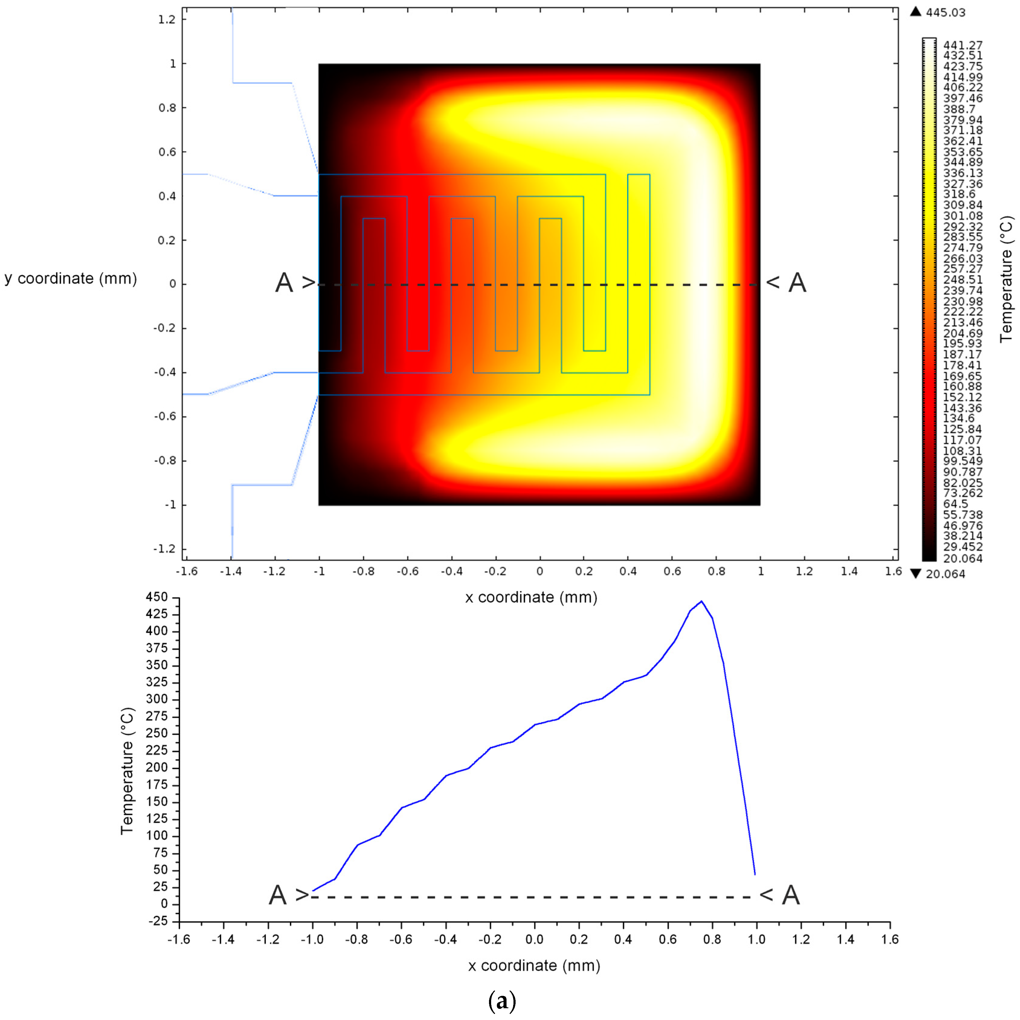
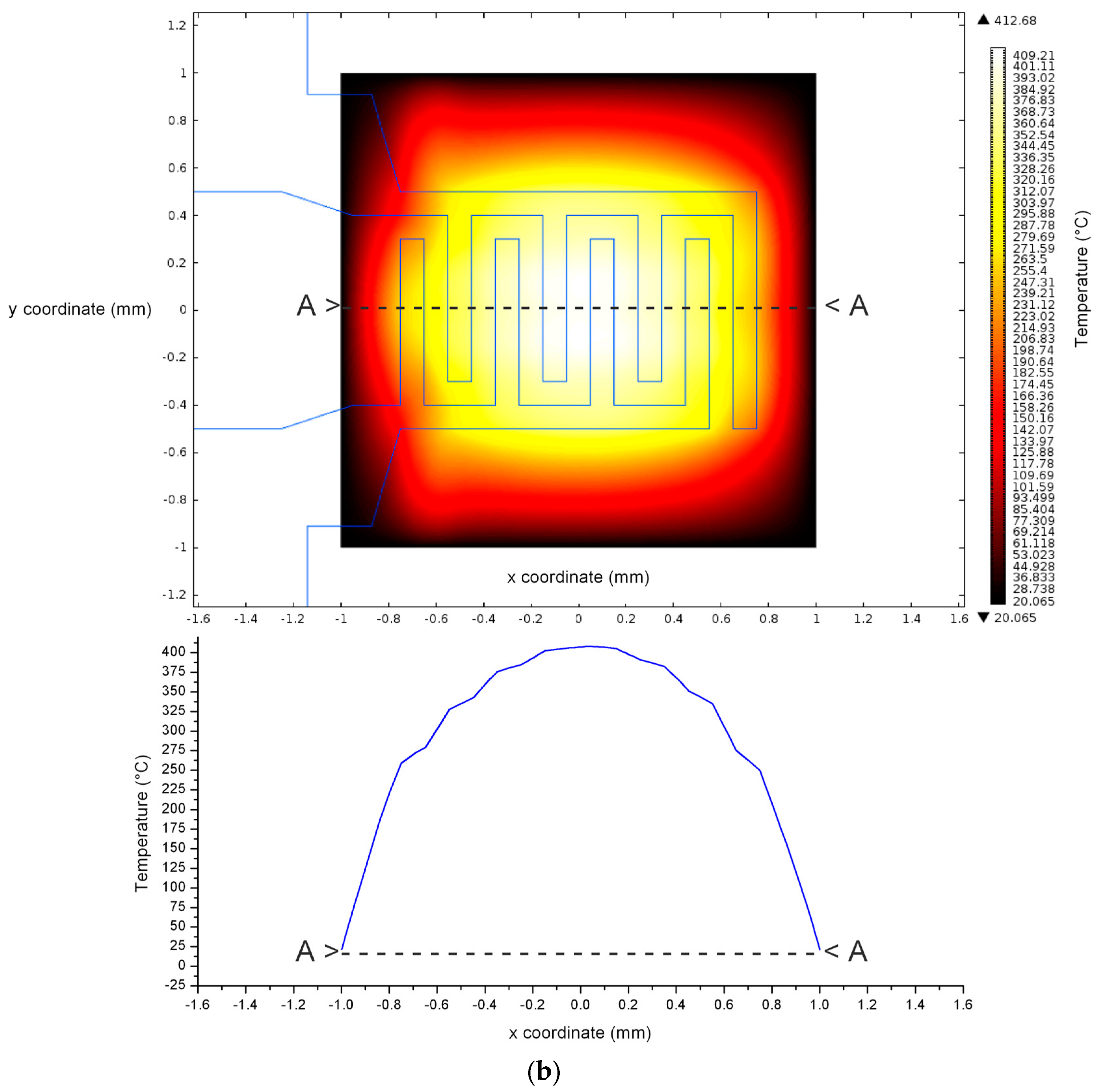
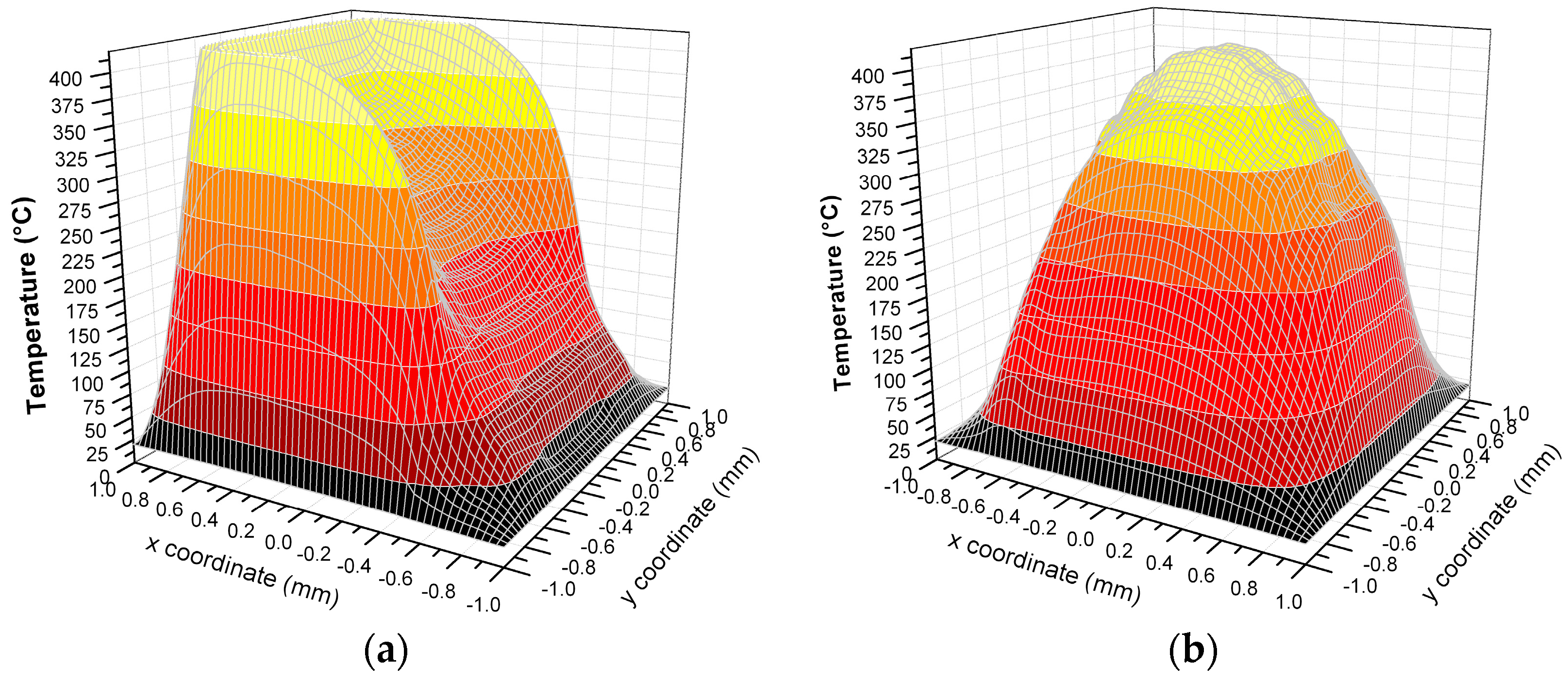
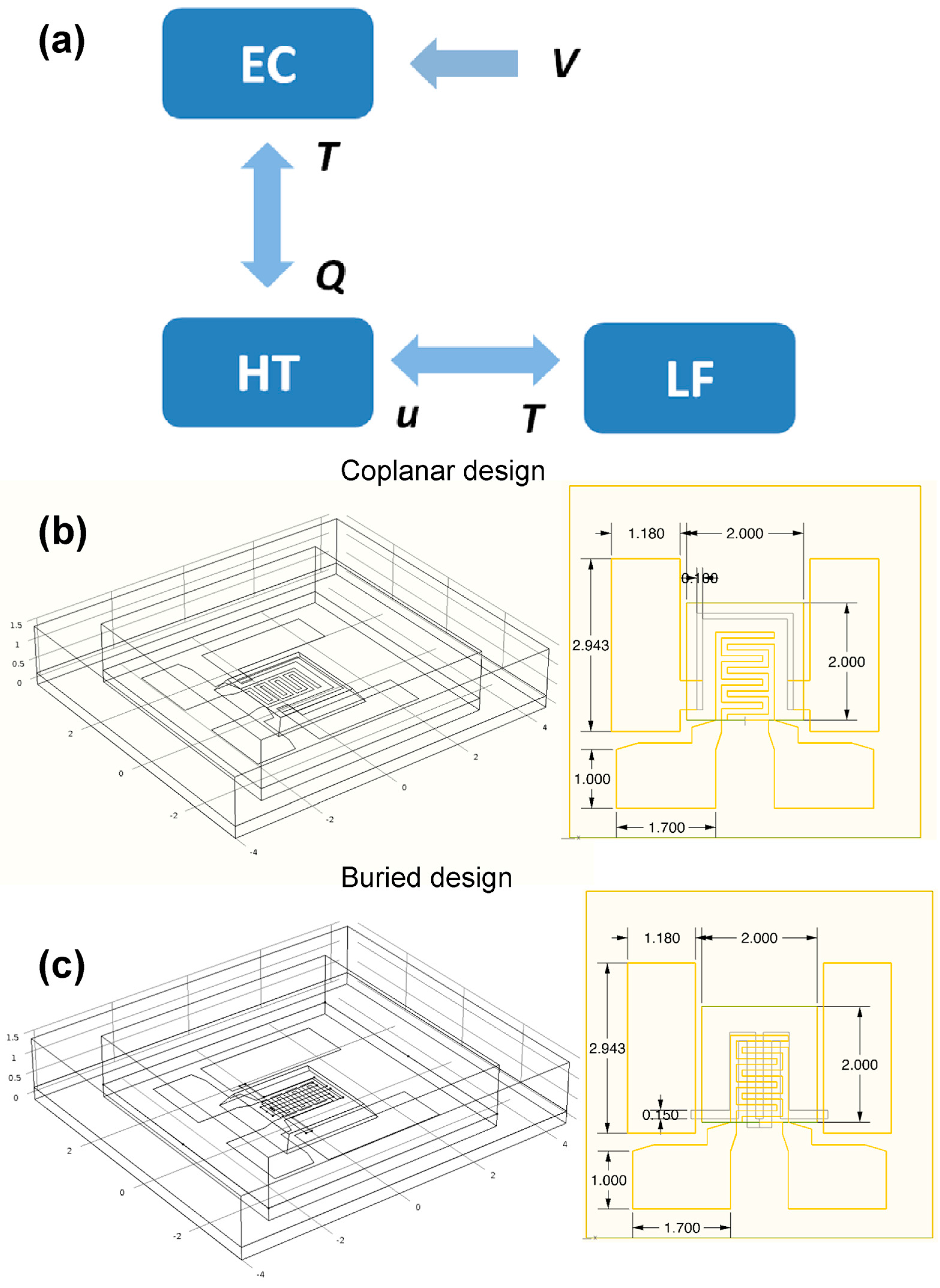
2.1. Design and FEM Models
- (A)
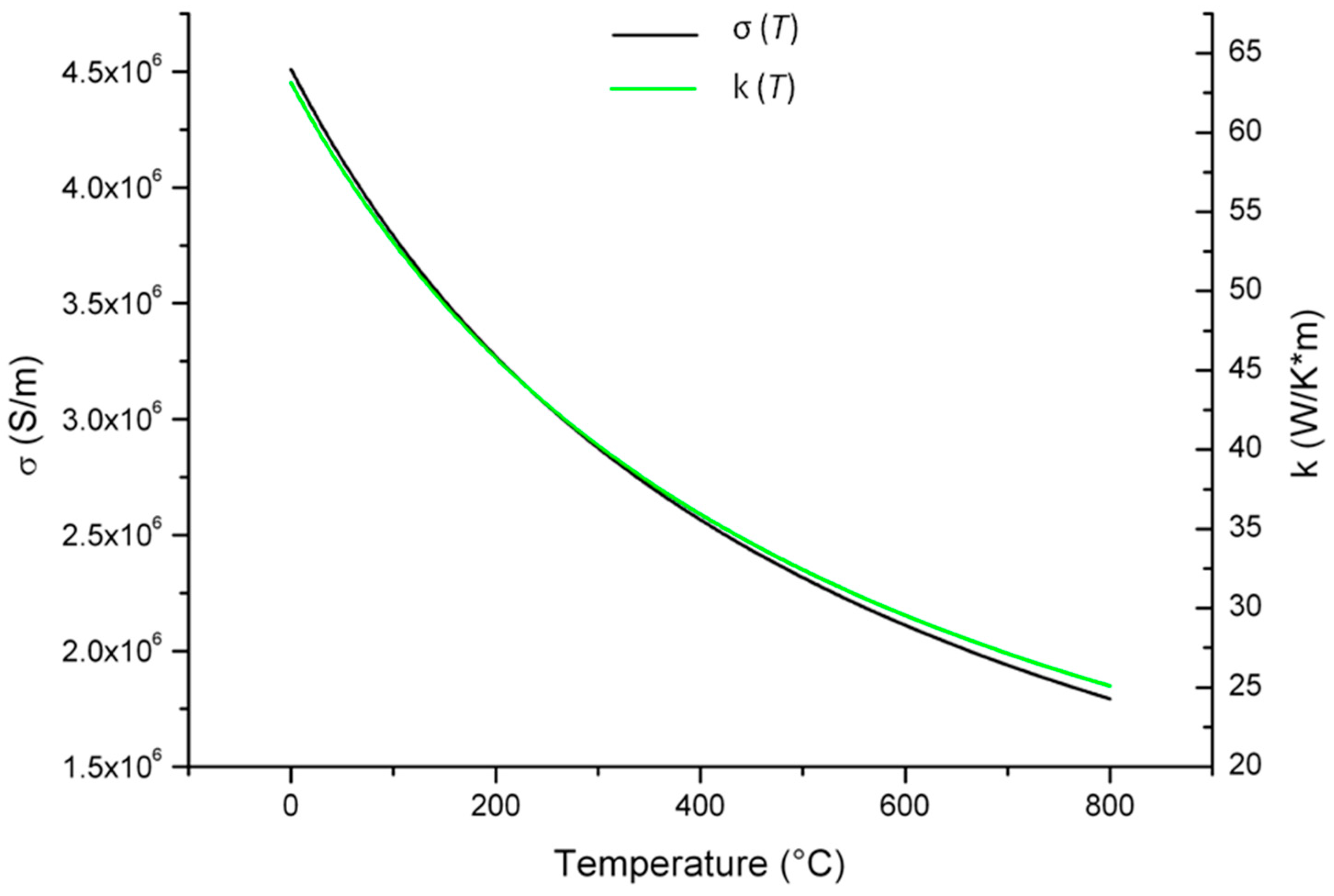
- the electrical current (EC):this equations set represents the dynamic currents equations for a time dependent study [21], J is the current density vector, Qj the charge, E the electric field, D the electric displacement field, V the electric potential, σ is the electrical material conductivity (Table 1), ε0 = 8.8541878176 × 10⁻¹² F/m is the vacuum permittivity, εr is the relative material permittivity (Table 1);
- (B)
- the heat transfer (HT):this equation represents the heat transfer in solids and fluids (air) [22], where Cp is the material mass capacitance (Table 1), T the temperature, u the displacement field, Q the heat flux, ρ is the material density (Table 1) and k is the material thermal conductivity (Table 1);
- (C)
- the laminar flow (LF):this equation set is used to simulate the fluids (air) movements forced by convection in the air box [22], where p is the pressure, μ the air dynamic viscosity, ρair the air density, I the unit tensor and F the external forces. In this case, the default air material properties retrieved by COMSOL Multiphysics® material library were used.
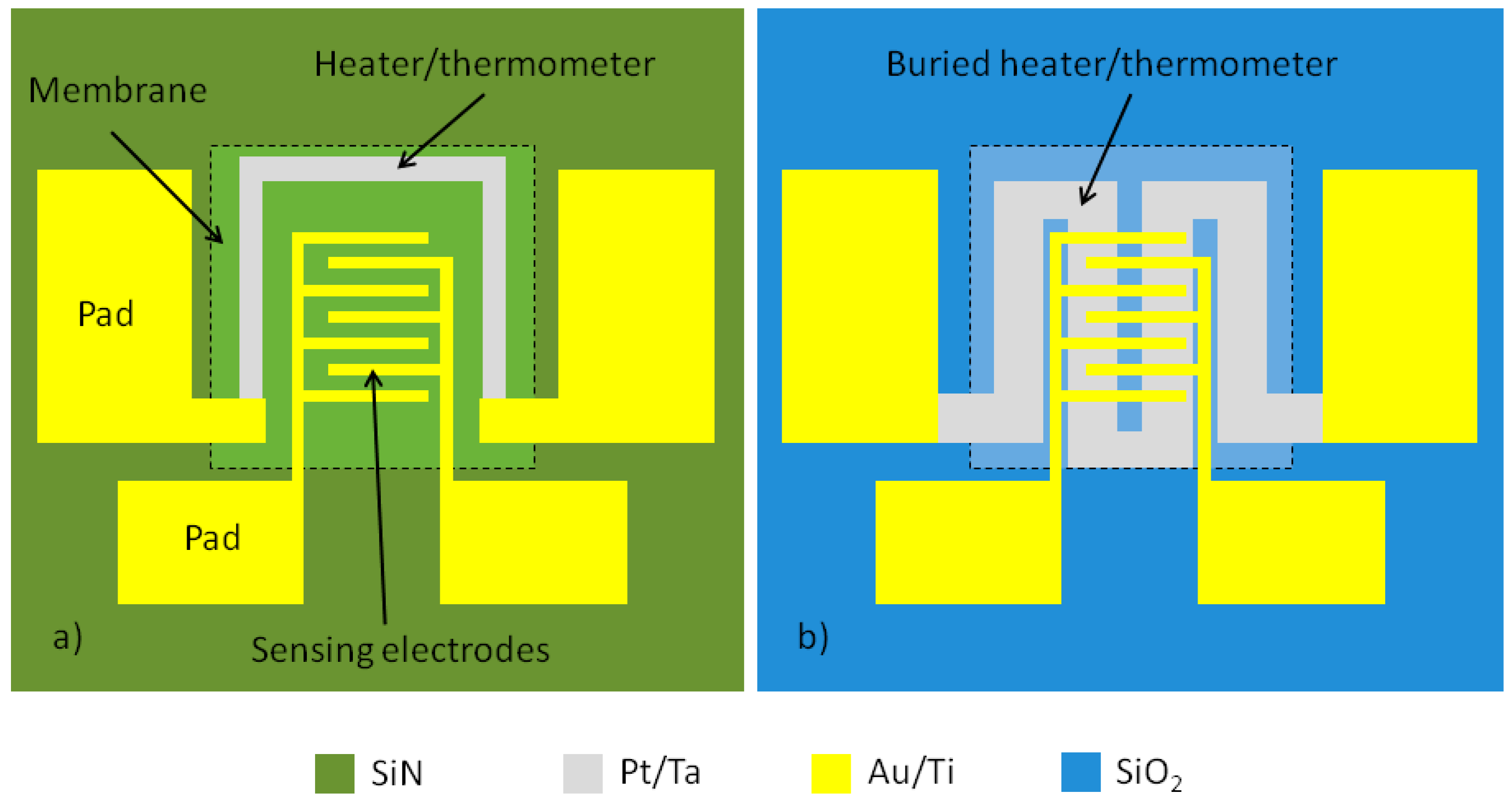
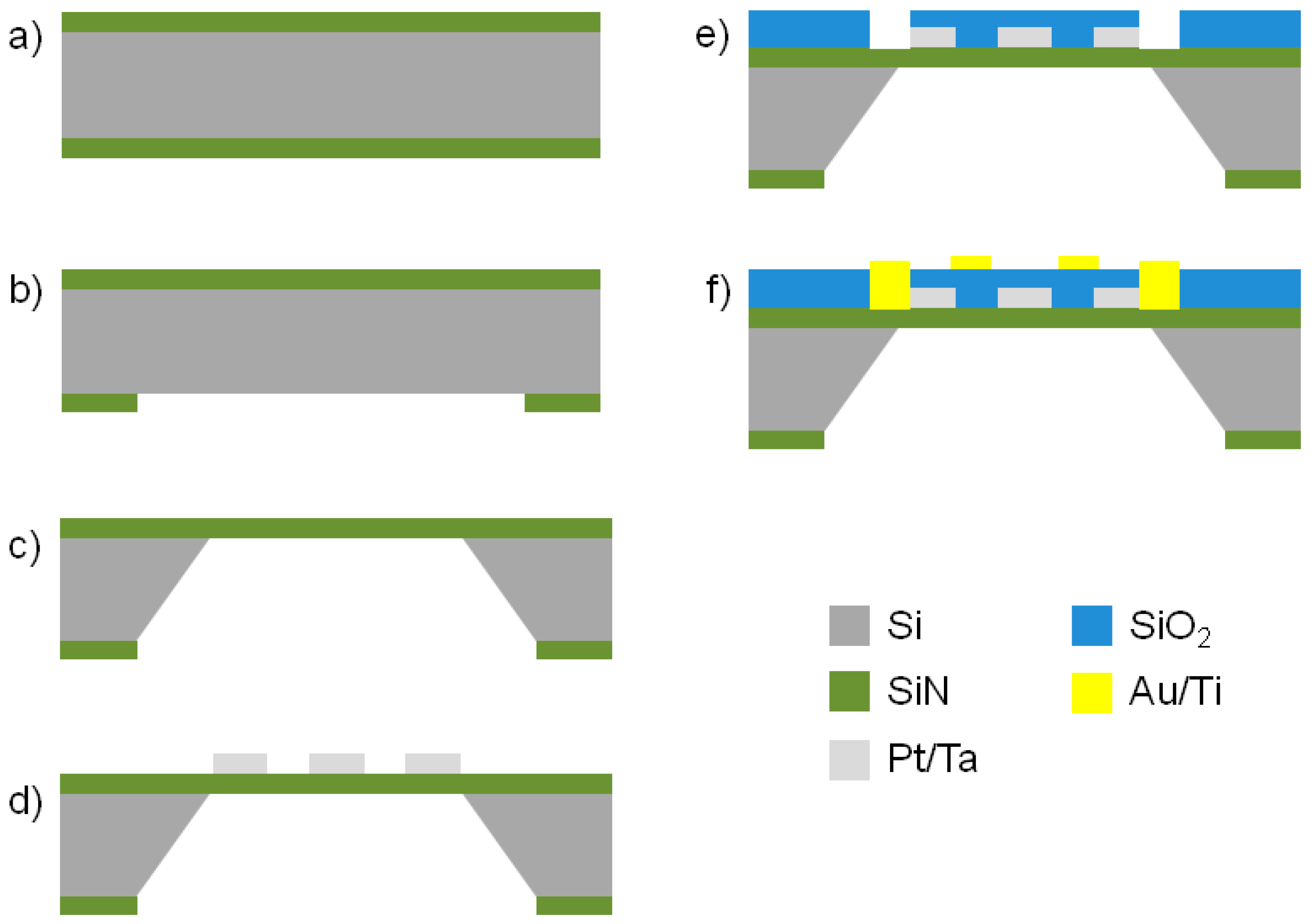
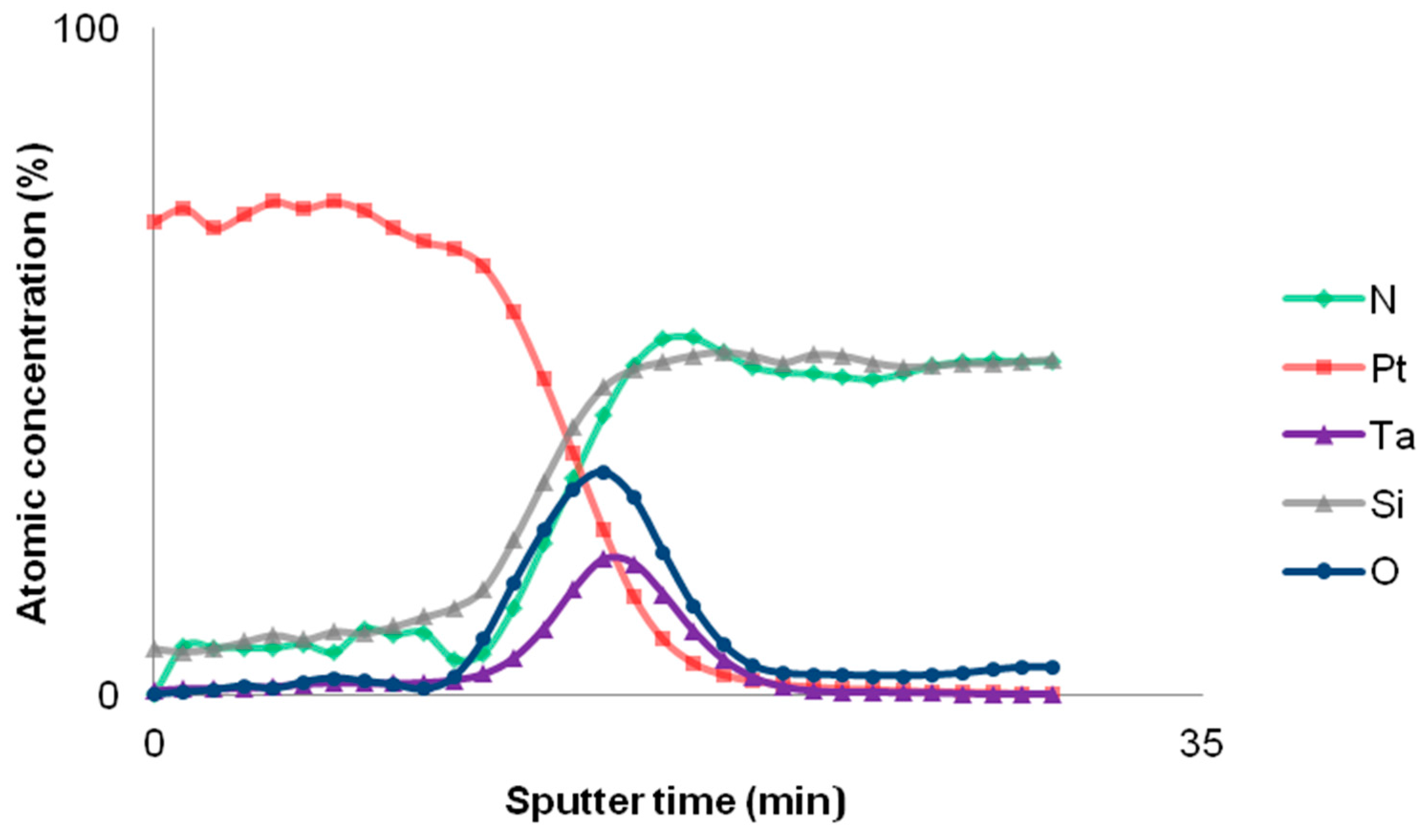
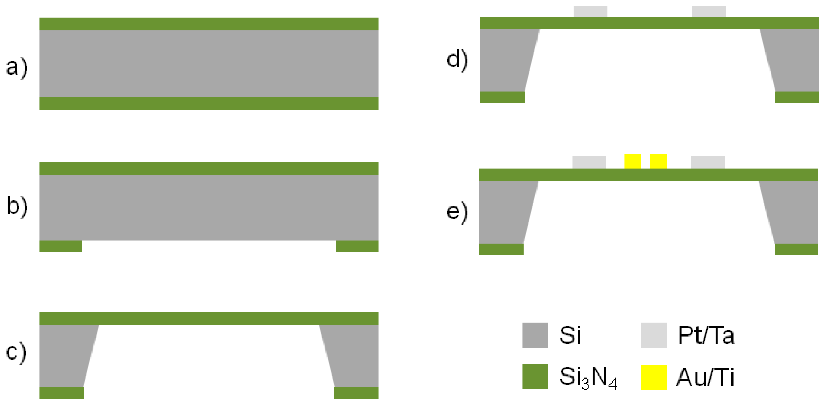
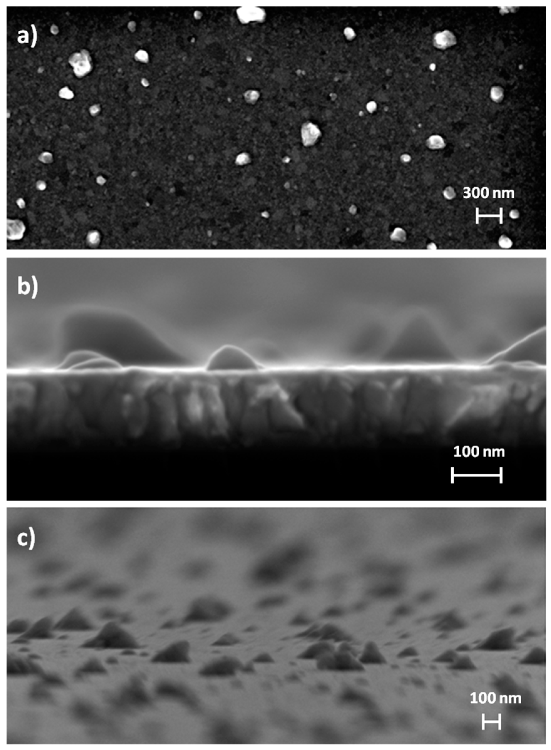
2.2. Coplanar Fabrication Approach
2.3. Buried Fabrication Approach
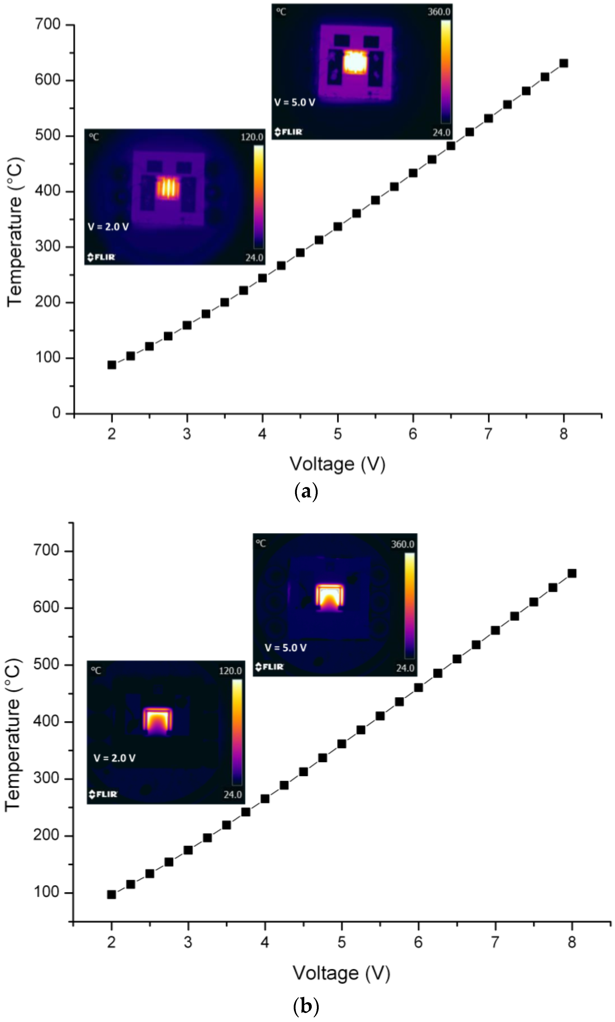
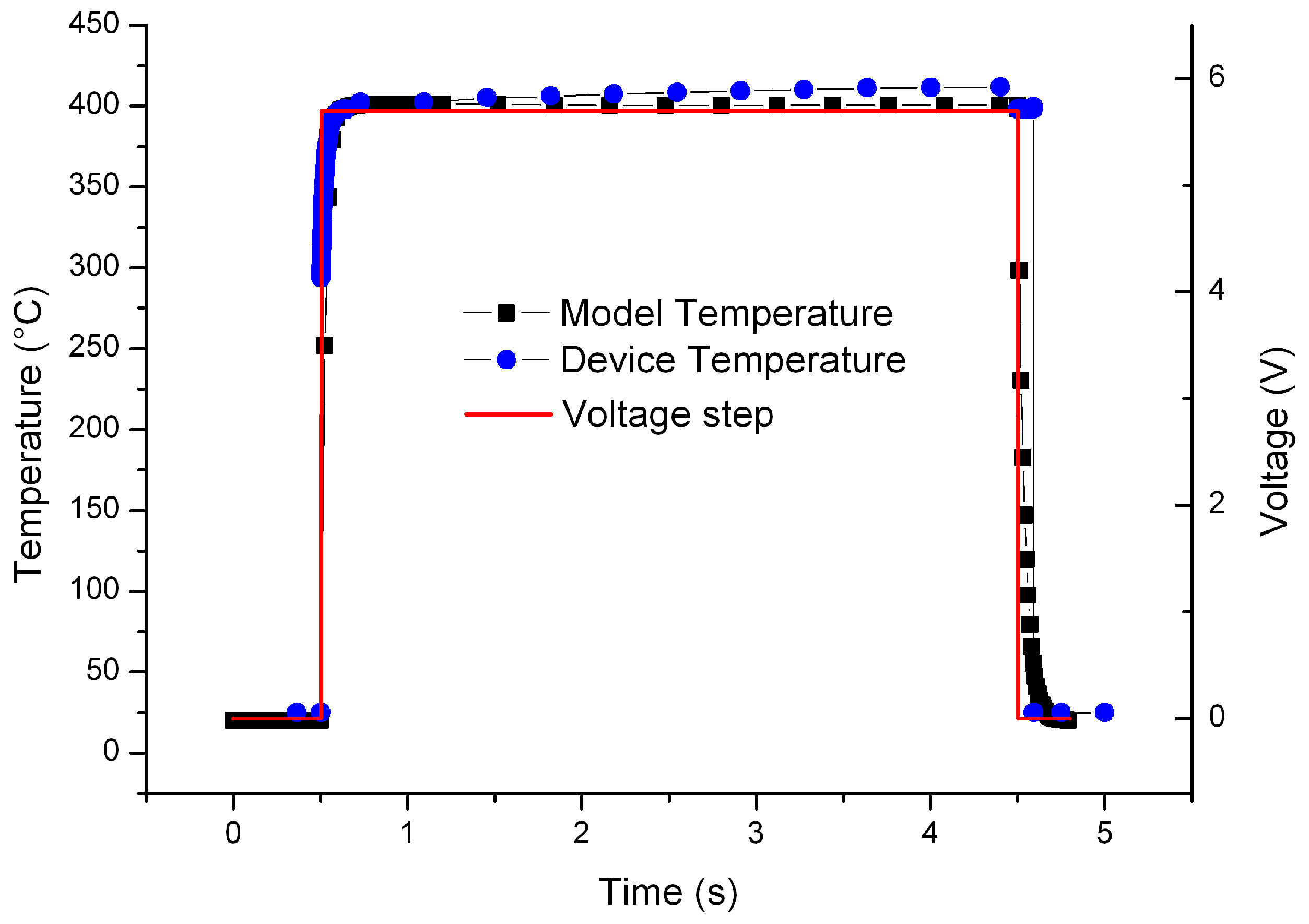
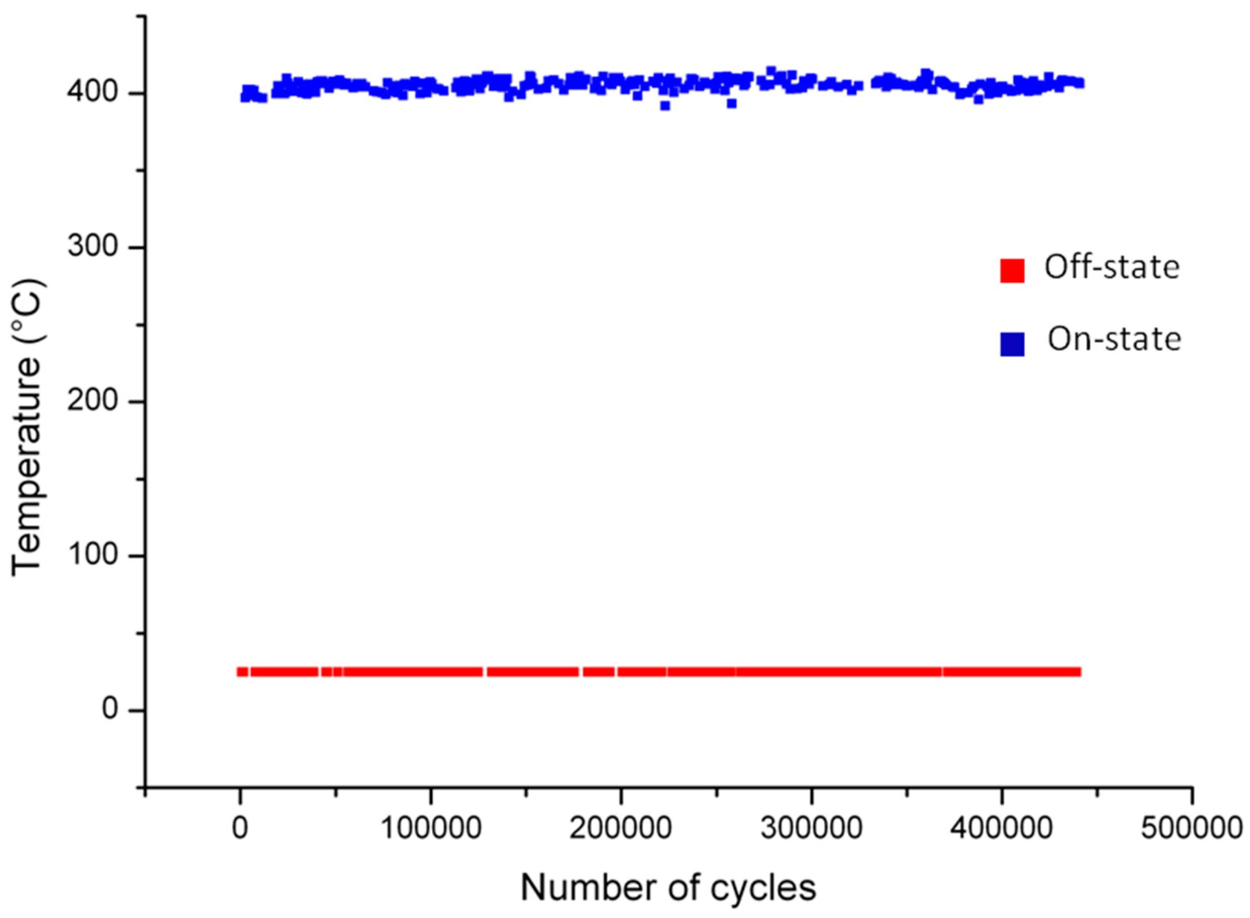
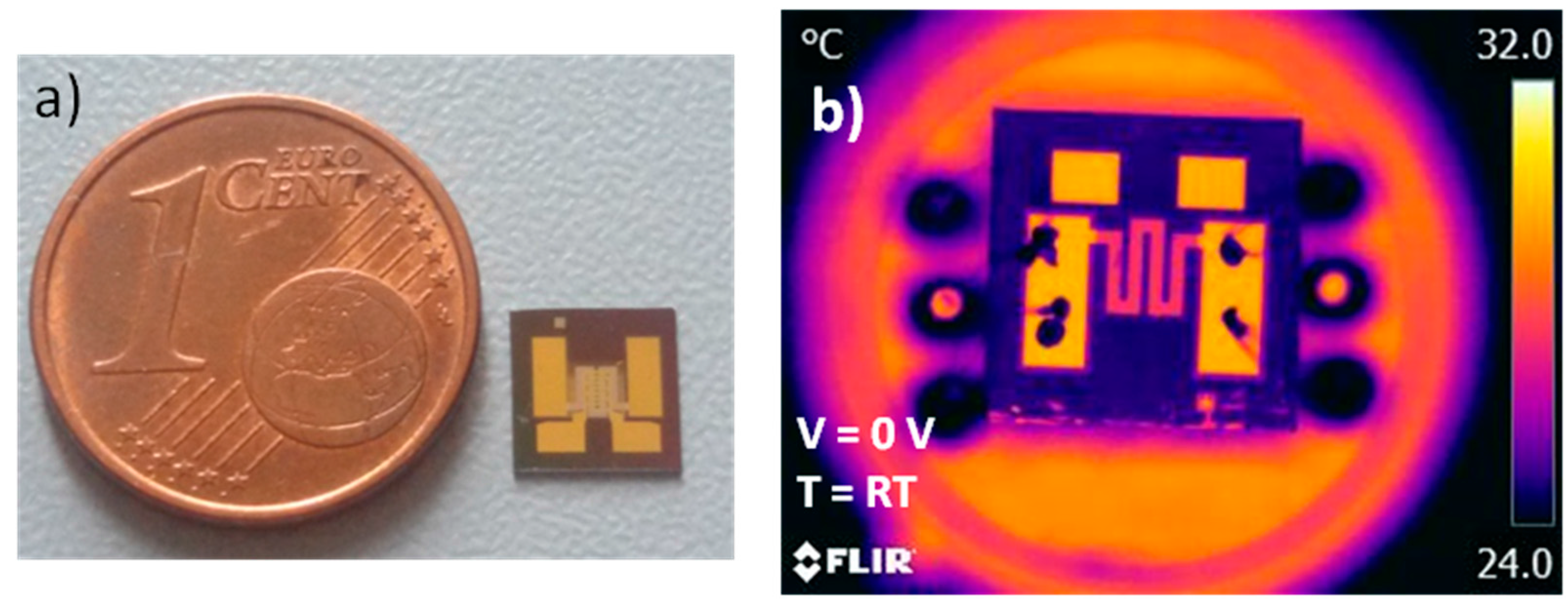
2.4. Device Characterization
3. Results and Discussion
4. Conclusions
Acknowledgments
Author Contributions
Conflicts of Interest
References
- Shen, G.; Chen, P.-C.; Ryu, K.; Zhou, C. Devices and chemical sensing applications of metal oxide nanowires. J. Mater. Chem. 2009, 19, 828–839. [Google Scholar] [CrossRef]
- Gad-el-Hak, M.; Seemann, W. MEMS Handbook. Appl. Mech. Rev. 2002, 55, B109. [Google Scholar] [CrossRef]
- Ali, S.Z.; Udrea, F.; Milne, W.I.; Gardner, J.W. Tungsten-based SOI microhotplates for smart gas sensors. J. Microelectromech. Syst. 2008, 17, 1408–1417. [Google Scholar] [CrossRef]
- Beckel, D.; Briand, D.; Bieberle-Hütter, A.; Courbat, J.; de Rooij, N.F.; Gauckler, L.J. Micro-hotplates-A platform for micro-solid oxide fuel cells. J. Power Sources 2007, 166, 143–148. [Google Scholar] [CrossRef]
- Rettig, F.; Moos, R. Ceramic meso hot-plates for gas sensors. Sens. Actuators B Chem. 2004, 103, 91–97. [Google Scholar] [CrossRef]
- Briand, D.; Colin, S.; Gangadharaiah, A.; Vela, E.; Dubois, P.; Thiery, L.; de Rooij, N.F. Micro-hotplates on polyimide for sensors and actuators. Sens. Actuators A Phys. 2006, 132, 317–324. [Google Scholar] [CrossRef]
- Sberveglieri, G.; Hellmich, W.; Müller, G. Silicon hotplates for metal oxide gas sensor elements. Microsyst. Technol. 1997, 3, 183–190. [Google Scholar] [CrossRef]
- Ivanov, P.; Stankova, M.; Llobet, E.; Vilanova, X.; Brezmes, J.; Gràcia, I.; Cané, C.; Calderer, J.; Correig, X. Nanoparticle metal-oxide films for micro-hotplate-based gas sensor systems. IEEE Sens. J. 2005, 5, 798–808. [Google Scholar] [CrossRef]
- Walden, P.; Kneer, J.; Knobelspies, S.; Kronast, W.; Mescheder, U.; Palzer, S. Micromachined Hotplate Platform for the Investigation of Ink-Jet Printed, Functionalized Metal Oxide Nanoparticles. J. Microelectromech. Syst. 2015, 24, 1384–1390. [Google Scholar] [CrossRef]
- Annanouch, F.E.; Gràcia, I.; Figueras, E.; Llobet, E.; Cané, C.; Vallejos, S. Localized aerosol-assisted CVD of nanomaterials for the fabrication of monolithic gas sensor microarrays. Sens. Actuators B Chem. 2015, 216, 374–383. [Google Scholar] [CrossRef]
- Marasso, S.L.; Tommasi, A.; Perrone, D.; Cocuzza, M.; Mosca, R.; Villani, M.; Zappettini, A.; Calestani, D. A new method to integrate ZnO nano-tetrapods on MEMS micro-hotplates for large scale gas sensor production. Nanotechnology 2016, 27, 1–7. [Google Scholar] [CrossRef] [PubMed]
- Tommasi, A.; Coletta, G.; Balma, D.; Marasso, S.L.; Perrone, D.; Canavese, G.; Stassi, S.; Bianco, S.; Cocuzza, M.; Pirri, C.F. Process optimisation of a MEMS based PZT actuated microswitch. Microelectron. Eng. 2014, 119, 137–140. [Google Scholar] [CrossRef]
- Balma, D.; Lamberti, A.; Marasso, S.L.L.; Perrone, D.; Quaglio, M.; Canavese, G.; Bianco, S.; Cocuzza, M. Piezoelectrically actuated MEMS microswitches for high current applications. Microelectron. Eng. 2011, 88, 2208–2210. [Google Scholar] [CrossRef]
- Adami, A.; Lorenzelli, L.; Guarnieri, V.; Francioso, L.; Forleo, A.; Agnusdei, G.; Taurino, A.M.; Zen, M.; Siciliano, P. A WO3-based gas sensor array with linear temperature gradient for wine quality monitoring. Sens. Actuators B Chem. 2006, 117, 115–122. [Google Scholar] [CrossRef]
- Francioso, L.; Forleo, A.; Taurino, A.M.; Siciliano, P.; Lorenzelli, L.; Guarnieri, V.; Adami, A.; Agnusdei, G. Linear temperature microhotplate gas sensor array for automotive cabin air quality monitoring. Sens. Actuators B Chem. 2008, 134, 660–665. [Google Scholar] [CrossRef]
- Khan, U.; Falconi, C. An accurate and computationally efficient model for membrane-type circular-symmetric micro-hotplates. Sensors 2014, 14, 7374–7393. [Google Scholar] [CrossRef] [PubMed]
- Canavese, G.; Ricci, A.; Gazzadi, G.C.; Ferrante, I.; Mura, A.; Marasso, S.L.; Ricciardi, C. Resonating Behaviour of Nanomachined Holed Microcantilevers. Sci. Rep. 2015, 5, 17837. [Google Scholar] [CrossRef] [PubMed]
- Chiolerio, A.; Ferrante, I.; Ricci, A.; Marasso, S.; Tiberto, P.; Canavese, G.; Ricciardi, C.; Allia, P. Toward mechano-spintronics: Nanostructured magnetic multilayers for the realization of microcantilever sensors featuring wireless actuation for liquid environments. J. Intell. Mater. Syst. Struct. 2012, 24, 2189–2196. [Google Scholar] [CrossRef]
- Zhang, X.; Grigoropoulos, C.P. Thermal conductivity and diffusivity of free-standing silicon nitride thin films. Rev. Sci. Instrum. 1995, 66, 1115–1120. [Google Scholar] [CrossRef]
- Zhang, X.; Xie, H.; Fujii, M.; Ago, H.; Takahashi, K.; Ikuta, T.; Abe, H.; Shimizu, T. Thermal and electrical conductivity of a suspended platinum nanofilm. Appl. Phys. Lett. 2005, 86, 1–3. [Google Scholar] [CrossRef]
- Ida, N. Engineering Electromagnetics; Springer International Publishing: Cham, Switzerland, 2015. [Google Scholar]
- Incropera, F.P.; DeWitt, D.P.; Bergman, T.L.; Lavine, A.S. Fundamentals of Heat and Mass Transfer; John Wiley & Sons Inc.: Hoboken, NJ, USA, 2007; Volume 6. [Google Scholar]
- Tiggelaar, R.M.; Sanders, R.G.P.; Groenland, A.W.; Gardeniers, J.G.E. Stability of thin platinum films implemented in high-temperature microdevices. Sens. Actuators A Phys. 2009, 152, 39–47. [Google Scholar] [CrossRef]
- Vilquin, B.; Le Rhun, G.; Bouregba, R.; Poullain, G.; Murray, H. Effect of in situ Pt bottom electrode deposition and of Pt top electrode preparation on PZT thin films properties. Appl. Surf. Sci. 2002, 195, 63–73. [Google Scholar] [CrossRef]
- Tiggelaar, R.M.; van Male, P.; Berenschot, J.W.; Gardeniers, J.G.E.; Oosterbroek, R.E.; de Croon, M.H.J.M.; Schouten, J.C.; van den Berg, A.; Elwenspoek, M.C. Fabrication of a high-temperature microreactor with integrated heater and sensor patterns on an ultrathin silicon membrane. Sens. Actuators A Phys. 2005, 119, 196–205. [Google Scholar] [CrossRef]
- Muralt, P.; Kohli, M.; Maeder, T.; Kholkin, A.; Brooks, K.; Setter, N.; Luthier, R. Fabrication and characterization of PZT thin-film vibrators for micromotors. Sens. Actuators A Phys. 1995, 48, 157–165. [Google Scholar] [CrossRef]
- Sreenivas, K.; Reaney, I.; Maeder, T.; Setter, N.; Jagadish, C.; Elliman, R.G. Investigation of Pt/Ti bilayer metallization on silicon for ferroelectric thin film integration. J. Appl. Phys. 1994, 75, 232–239. [Google Scholar] [CrossRef]
- Cabral, C.; Clevenger, L.A.; Schad, R.G. Compressive Stress Increase With Repeated Thermal Cycling in Tantalum (Oxygen) Thin Films. MRS Proc. 1993, 308. [Google Scholar] [CrossRef]
- Matsui, Y.; Hiratani, M.; Kumagai, Y.; Miura, H.; Fujisaki, Y. Thermal stability of Pt bottom electrodes for ferroelectric capacitors. Jpn. J. Appl. Phys. Part 2 Lett. 1998, 37, L465–L467. [Google Scholar] [CrossRef]
- Spierings, G.A.C.M.; Breed, J.M.; Ulenaers, M.J.E.; van Veldhoven, P.J.; Larsen, P.K. Stresses in Ru/PbZr0.4Ti0.6O3/Ru thin film stacks for integrated ferroelectric capacitors. Microelectron. Eng. 1995, 29, 235–238. [Google Scholar] [CrossRef]
- Nam, H.J.; Choi, D.K.; Lee, W.J. Formation of hillocks in Pt/Ti electrodes and their effects on short phenomena of PZT films deposited by reactive sputtering. Thin Solid Films 2000, 371, 264–271. [Google Scholar] [CrossRef]
- Jung, W.W.; Choi, S.K.; Kweon, S.Y.; Yeom, S.J. Platinum (100) hillock growth in Pt/Ti electrode stack for SrBi 2Ta2O9 ferroelectric random access memory. J. Electroceram. 2004, 13, 55–63. [Google Scholar] [CrossRef]
- Maher, A.; Velusamy, V.; Riordan, D.; Walsh, J. Modelling of temperature coefficient of resistance of a thin film RTD towards exhaust gas measurement applications. In Proceedings of the 8th International Conference on Sensing Technology, Liverpool, UK, 2–4 September 2014; pp. 19–22.


| Property (Units) | Materials | |||
|---|---|---|---|---|
| Si | SiN | Au | Pt | |
| Density ρ (kg/m3) | 2330 | 3100 | 19,300 | 21,450 |
| Rel. permittivity εr | 11.7 | 9.7 | 1 | 1 |
| El. Conductivity σ (S/m) | 0.1 | 10−5 | 2.5 × 10⁷ | σ (T) |
| Specific Heat Cp (J/(kg·K)) | 700 | 700 | 129 | 133 |
| Th. Conductivity k (W/(m·K)) | 130 | 6 [19] | 160 | k (T) |
© 2016 by the authors; licensee MDPI, Basel, Switzerland. This article is an open access article distributed under the terms and conditions of the Creative Commons Attribution (CC-BY) license (http://creativecommons.org/licenses/by/4.0/).
Share and Cite
Tommasi, A.; Cocuzza, M.; Perrone, D.; Pirri, C.F.; Mosca, R.; Villani, M.; Delmonte, N.; Zappettini, A.; Calestani, D.; Marasso, S.L. Modeling, Fabrication and Testing of a Customizable Micromachined Hotplate for Sensor Applications. Sensors 2017, 17, 62. https://doi.org/10.3390/s17010062
Tommasi A, Cocuzza M, Perrone D, Pirri CF, Mosca R, Villani M, Delmonte N, Zappettini A, Calestani D, Marasso SL. Modeling, Fabrication and Testing of a Customizable Micromachined Hotplate for Sensor Applications. Sensors. 2017; 17(1):62. https://doi.org/10.3390/s17010062
Chicago/Turabian StyleTommasi, Alessio, Matteo Cocuzza, Denis Perrone, Candido Fabrizio Pirri, Roberto Mosca, Marco Villani, Nicola Delmonte, Andrea Zappettini, Davide Calestani, and Simone Luigi Marasso. 2017. "Modeling, Fabrication and Testing of a Customizable Micromachined Hotplate for Sensor Applications" Sensors 17, no. 1: 62. https://doi.org/10.3390/s17010062