
Programmable Low-Power Low-Noise Capacitance to Voltage Converter for MEMS Accelerometers

Abstract
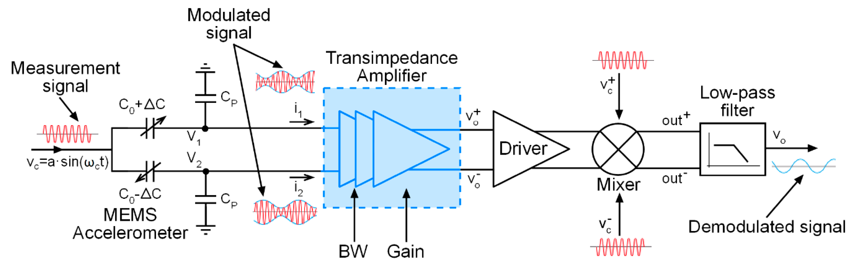
:1. Introduction
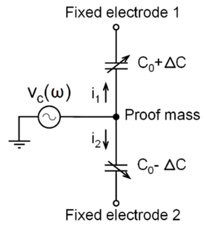
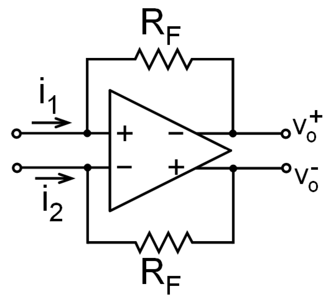
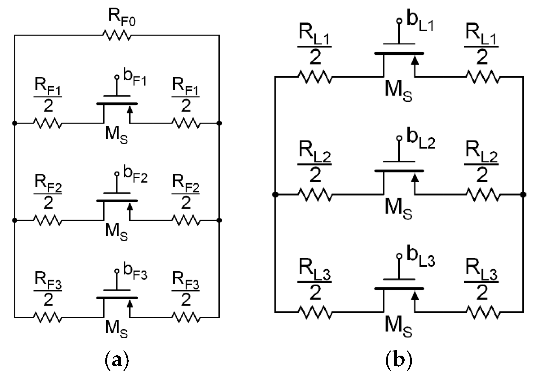
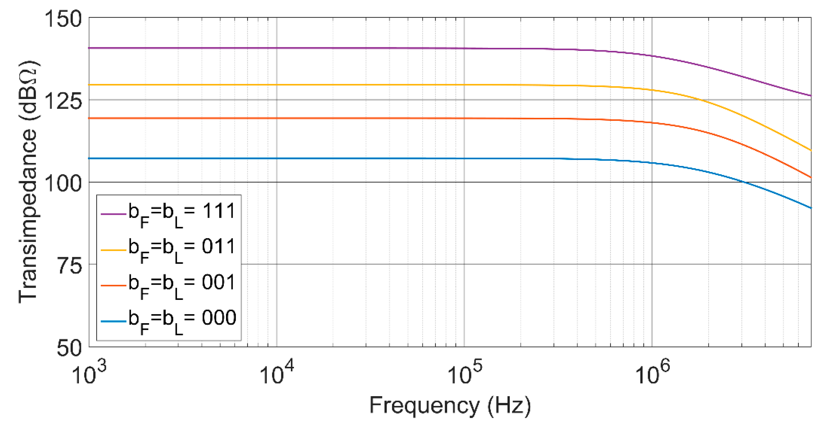
2. Capacitance to Voltage Converter
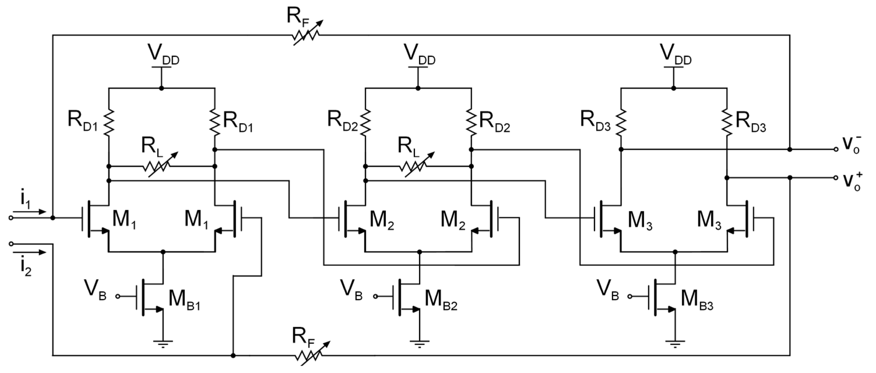
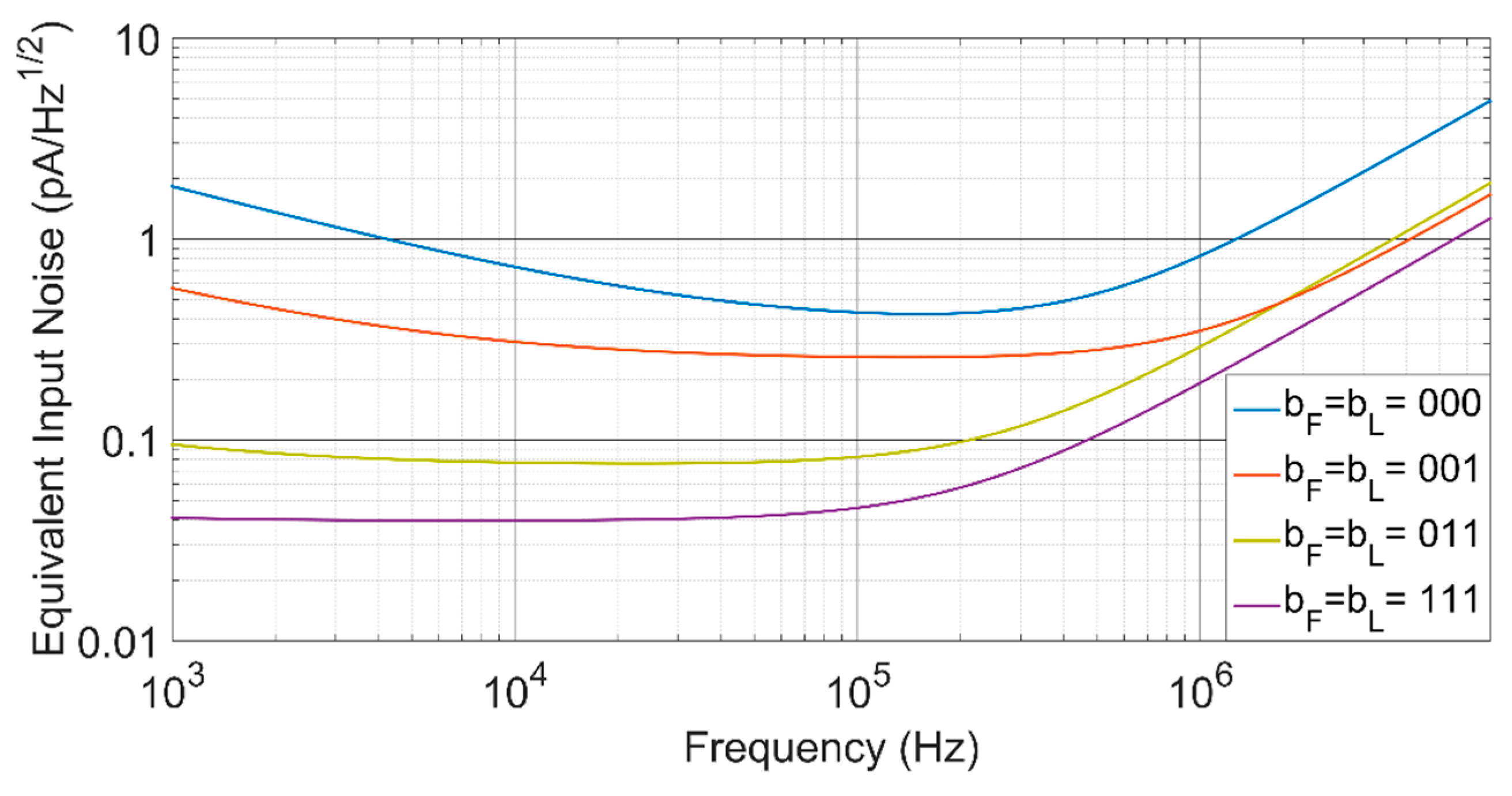
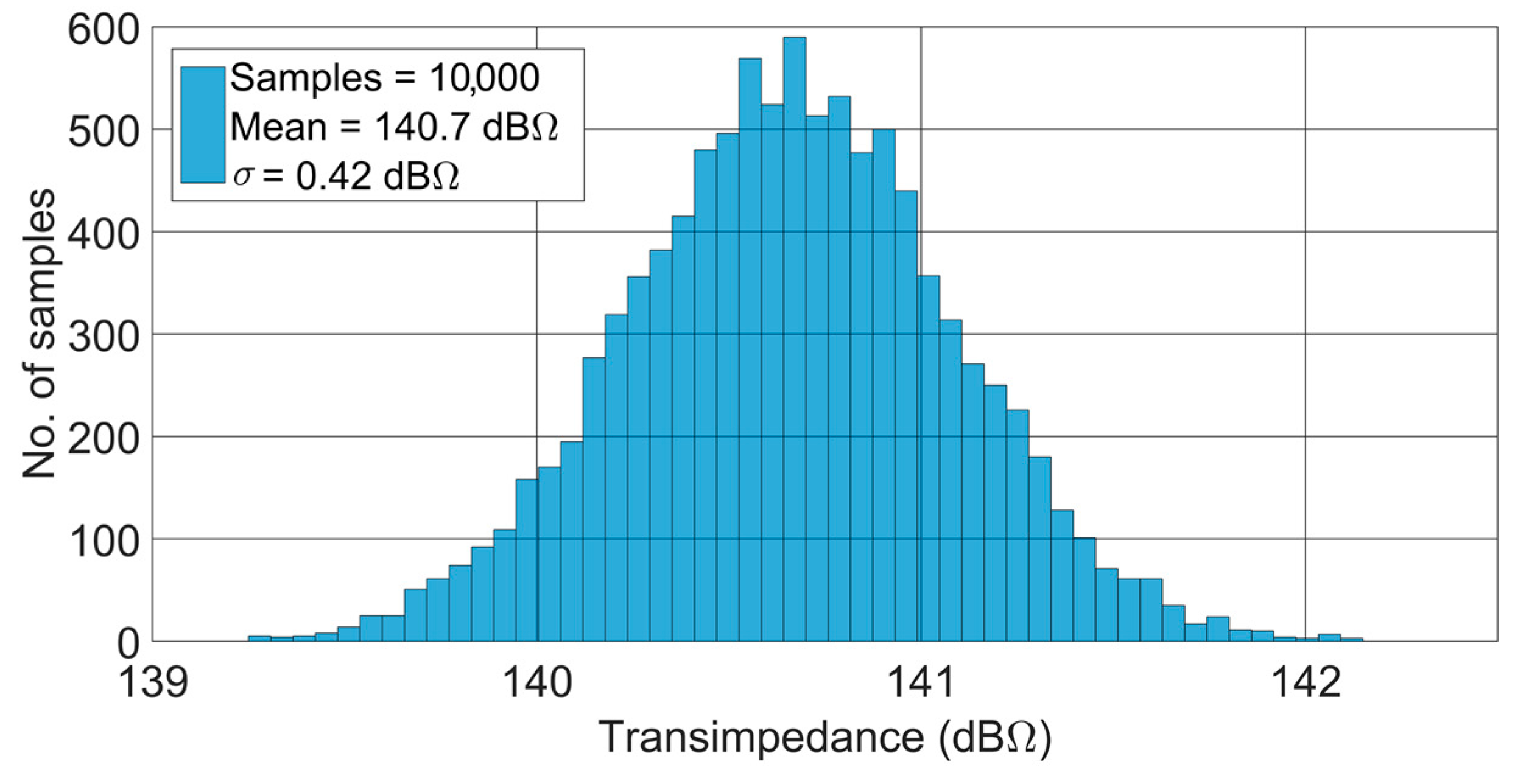
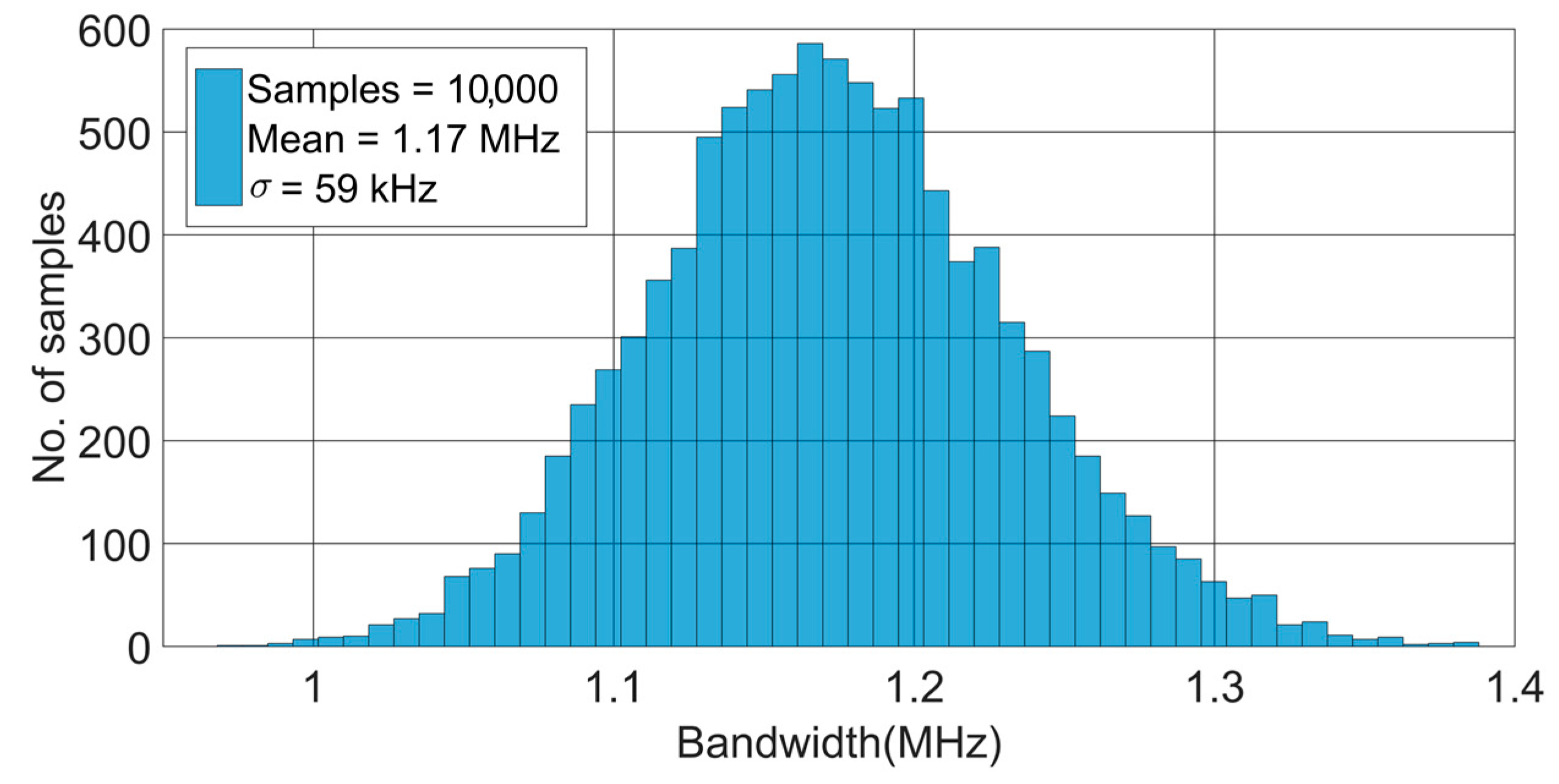
Transimpedance Amplifier Design
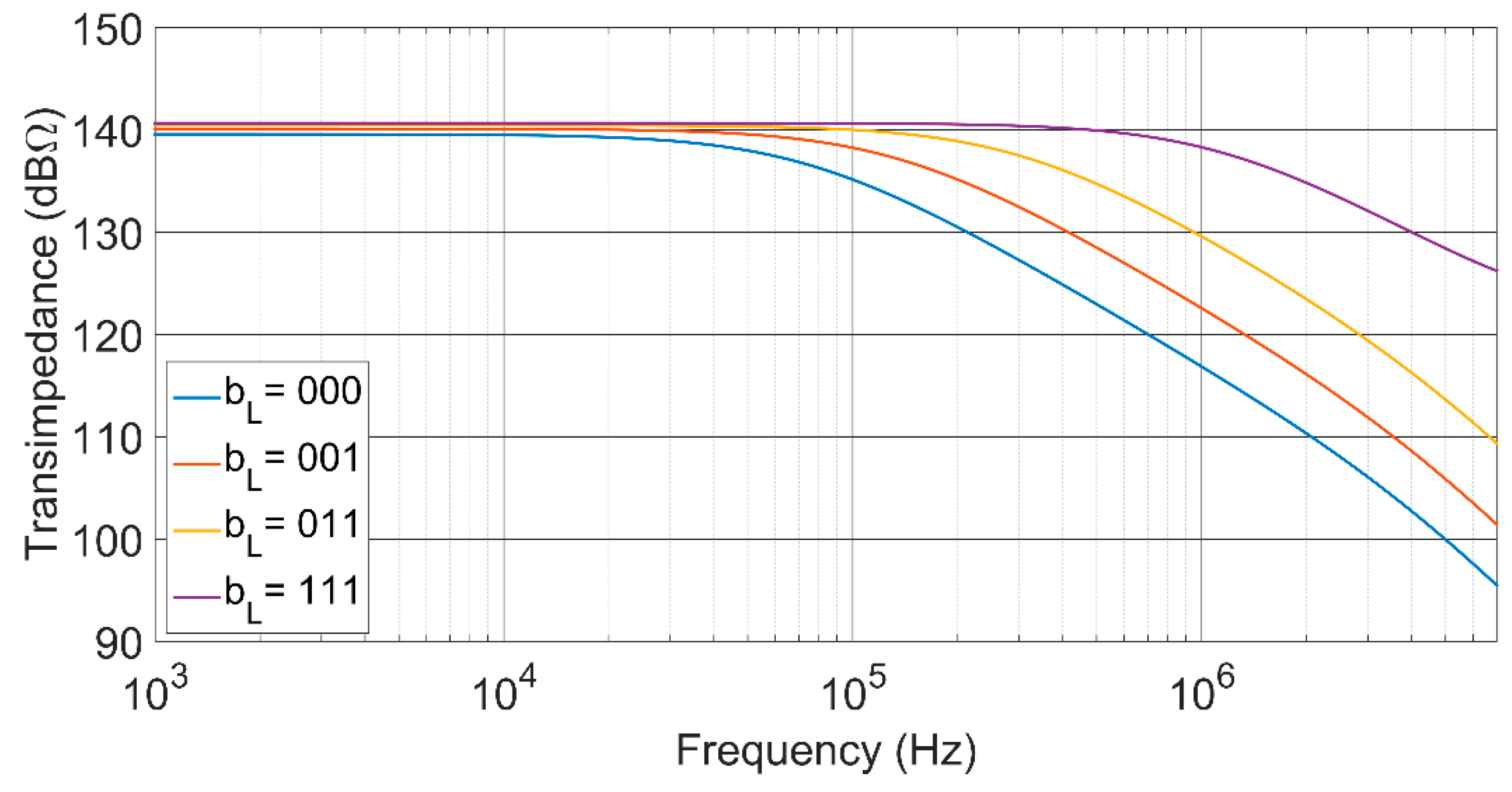
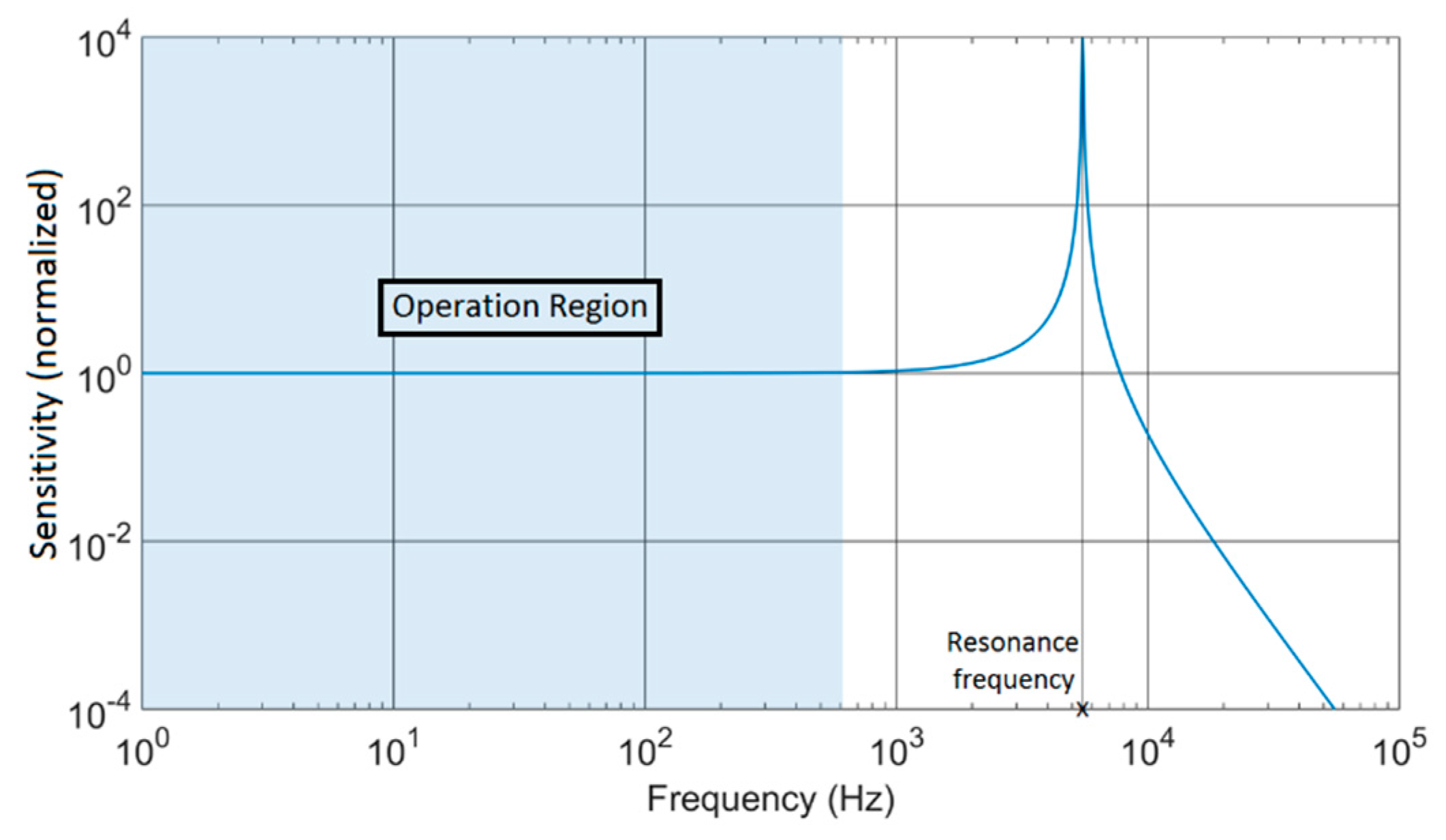
3. Discussion
4. Conclusions
Acknowledgments
Author Contributions
Conflicts of Interest
References
- Kaajakari, V. Capacitive sensing. In Practical Mems; Small Gear Publishing: Las Vegas, NV, USA, 2009; pp. 91–108. [Google Scholar]
- Eddy, D.S.; Sparks, D.R. Application of MEMS technology in automotive sensors and actuators. Proc. IEEE 1998, 86, 1747–1755. [Google Scholar] [CrossRef]
- Béliveau, A.; Spencer, G.T.; Thomas, K.A.; Roberson, S.L. Evaluation of MEMS capacitive accelerometers. IEEE Des. Test. Comput. 2002, 16, 48–56. [Google Scholar] [CrossRef]
- Tez, S.; Aykutlu, U.; Torunbalci, M.M.; Akin, T. A bulk-micromachined three-axis capacitive MEMS accelerometer on a single die. J. Microelectromec. Syst. 2015, 24, 1264–1274. [Google Scholar] [CrossRef]
- Aydin, O.; Akin, T. A bulk-micromachined fully differential MEMS accelerometer with split interdigitated fingers. IEEE Sens. J. 2013, 13, 2914–2921. [Google Scholar] [CrossRef]
- Göenenli, I.E.; Celik-Butler, Z.; Butler, D.P. Surface micromachined MEMS accelerometers on flexible polymide substrate. IEEE Sens. J. 2011, 11, 2318–2326. [Google Scholar] [CrossRef]
- Pakula, L.S.; Yang, H.; French, P.J. 3-D silicon carbide surface micromachined accelerometer compatible with CMOS processing. In Proceedings of the Seventh International Conference on Advanced Semiconductor Devices and Microsystems, Smolenice, Slovakia, 12–16 October 2008; pp. 227–230.
- Chen, L.; Li, Z.; Wang, Z. A 10-Gb/s 0.18-μm CMOS optical receiver front-end amplifier. In Proceedings of the 15th Asia-Pacific Conference on Communications, Shanghai, China, 8–10 October 2009.
- Liu, R.; Wang, Z.; Tian, J.; Meng, Z. A 57 dBΩ 1 GHz CMOS front-end preamplifier for optical receivers. In Proceedings of the 2012 8th International Conference on Wireless Communications, Networking and Mobile Computing, Shanghai, China, 21–23 September 2012.
- Lu, T.T.; Lee, H.C.; Wang, C.S.; Wang, C.K. A 4.9-mW 4-Gb/s single-to-differential TIA with current-amplifying regulated cascode. In Proceedings of the 2012 International Symposium on VLSI Design, Automation, and Test, Hsinchu, Taiwan, 23–25 April 2012.
- Hu, J.; Kim, Y.B.; Ayers, J. A low power 100 MΩ CMOS front-end transimpedance amplifier for biosensing applications. In Proceedings of the 2010 53rd IEEE International Midwest Symposium on Circuits and Systems, Seattle, WA, USA, 1–4 August 2010.
- Chuah, J.H.; Holburn, D. Design of low-noise high-gain CMOS transimpedance amplifier for intelligent sensing of secondary electrons. IEEE Sens. J. 2015, 15, 5997–6004. [Google Scholar] [CrossRef]
- Sutry, N.T.; Dennis, J.O.; Khir, M.H.M.; Ahmed, A.Y.; Mian, M.U. A monolithic, low-noise, capacitive readout interface circuit for CMOS-MEMS resonator-based gravimetric chemical gas sensors. In Proceedings of the 2015 IEEE AFRICON, Addis Ababa, Ethiopia, 14–17 September 2015.
- Colinet, E.; Arcamone, J.; Niel, A.; Lorent, E.; Hentz, S.; Ollier, E. 100 MHz oscillator based on a low polarization voltage capacitive Lamé-mode MEMS resonator. In Proceedings of the 2010 IEEE International Frequency Control Symposium (FCS), Newport Beach, CA, USA, 1–4 June 2010; pp. 174–178.
- Aydemir, A.; Akin, T. Fabrication of a three-axis capacitive MEMS accelerometer on a single substrate. In Proceedings of the 2015 IEEE SENSORS, Busan, Korea, 1–4 November 2015.
- Momen, H.G.; Tavakoli, H.; Sani, E.A. A 3-axis MEMS capacitive accelerometer free of cross axis sensitivity. In Proceedings of the 24th Iranian Conference on Electrical Engineering (ICEE), Shiraz, Iran, 10–12 May 2016.
- Tan, S.S.; Liu, C.Y.; Yeh, L.K.; Chiu, Y.H.; Lu, M.S.C.; Hsu, K.Y.J. An integrated low-noise sensing circuit with efficient bias stabilization for CMOS MEMS capacitive accelerometers. IEEE Trans. Circuits Syst. I 2011, 58, 2661–2672. [Google Scholar] [CrossRef]
- Sanz, M.T.; García del Pozo, J.M.; Celma, S.; Sarmiento, A. Constant-bandwidth adaptive transimpedance amplifier. Electron. Lett. 2007, 43, 1451–1452. [Google Scholar] [CrossRef]
- Royo, G.; Sánchez-Azqueta, C.; Aldea, C.; Celma, S.; Gimeno, C. CMOS transimpedance amplifier with controllable gain for RF overlay. In Proceedings of the 12th Conference on Ph.D. Research in Microelectronics and Electronics, Lisbon, Portugal, 27–30 June 2016.
- Benmessaour, M.; Nasreddine, M.M. Optimization of MEMS capacitive accelerometer. Microsyst. Technol. 2013, 19, 713–720. [Google Scholar] [CrossRef]
- Salvia, J.; Lajevardi, P.; Hekmat, M.; Murmann, B. A 56 MΩ CMOS TIA for MEMS applications. In Proceedings of the IEEE 2009 Custom Integrated Circuits Conference, San Jose, CA, USA, 13–16 September 2009; pp. 199–202.
- Sharma, A.; Faisal Zaman, M.; Ayazi, F. A 104-dB dynamic range transimpedance-based CMOS ASIC for tuning fork microgyroscopes. J. Microelectromec. Syst. 2007, 42, 1790–1802. [Google Scholar] [CrossRef]
- Yin, T.; Wu, H.; Wu, Q.; Yang, H.; Jiao, J. A TIA-based readout circuit with temperature compensation for MEMS capacitive gyroscope. In Proceedings of the 2011 6th IEEE International Conference on Nano/Micro Engineered and Molecular Systems, Kaohsiung, Taiwan, 20–23 February 2011; pp. 401–405.


| 20 μm/1 μm | 20 μm/0.5 μm | 10 μm/1 μm | 10.5 μm/4 μm | 20 μm/0.18 μm | 180 kΩ | 600 mV |
| 5 MΩ | 1.1 MΩ | 380 kΩ | 100 kΩ | 33 kΩ | 48 kΩ | 45 kΩ |
| [17] 1 | [21] 2 | [22] 1 | [23] 2 | This Work 2 | |
|---|---|---|---|---|---|
| Technology | 0.35 μm CMOS | 0.18 μm CMOS | 0.6 μm CMOS | 0.35 μm CMOS | 0.18 μm CMOS |
| Supply Voltage | 3.3 V | 1.8 V | 3 V | 5 V | 1.8 V |
| Minimum Input Noise | 54 μg/ | 65 fA/ | 88 fA/ | 63 fA/ * | 42 fA/ |
| Capacitive Sensitivity | 1450 mV/fF* (18 mV/fF without PA) | - | 25 mV/fF * | 3.3 mV/fF | 1 mV/fF |
| Power Consumption | 5.1 mW | 436 μW | 400 μW | - | 54 μW |
| Type of Sensing Interface | Voltage Amplifier | Capacitive TIA | Resistive TIA | Resistive TIA | Resistive TIA |
| Gain | −9 to +2 dB | 56 MΩ | 1.6–25 MΩ | 2–22 MΩ | 0.15–10 MΩ |
| Bandwidth | 8.6 MHz | 1.8 MHz | 200 kHz * | 200 kHz * | 75 kHz–1.2 MHz |
| Application | Accelerometer | Resonator/Oscillator | Gyroscope | Gyroscope | Accelerometer |
© 2016 by the authors; licensee MDPI, Basel, Switzerland. This article is an open access article distributed under the terms and conditions of the Creative Commons Attribution (CC-BY) license (http://creativecommons.org/licenses/by/4.0/).
Share and Cite
Royo, G.; Sánchez-Azqueta, C.; Gimeno, C.; Aldea, C.; Celma, S. Programmable Low-Power Low-Noise Capacitance to Voltage Converter for MEMS Accelerometers. Sensors 2017, 17, 67. https://doi.org/10.3390/s17010067
Royo G, Sánchez-Azqueta C, Gimeno C, Aldea C, Celma S. Programmable Low-Power Low-Noise Capacitance to Voltage Converter for MEMS Accelerometers. Sensors. 2017; 17(1):67. https://doi.org/10.3390/s17010067
Chicago/Turabian StyleRoyo, Guillermo, Carlos Sánchez-Azqueta, Cecilia Gimeno, Concepción Aldea, and Santiago Celma. 2017. "Programmable Low-Power Low-Noise Capacitance to Voltage Converter for MEMS Accelerometers" Sensors 17, no. 1: 67. https://doi.org/10.3390/s17010067