
Fully Printed Flexible Single-Chip RFID Tag with Light Detection Capabilities

 , and
, and
Abstract
:1. Introduction
2. Materials and Methods
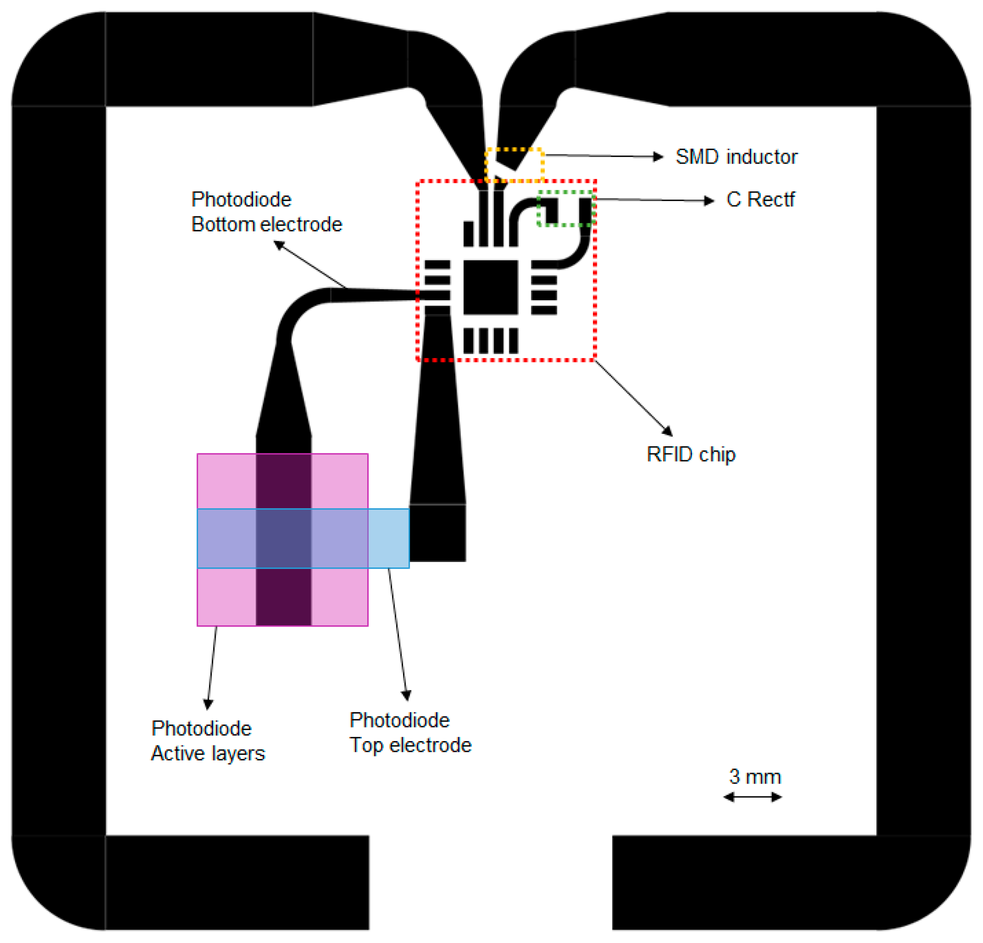
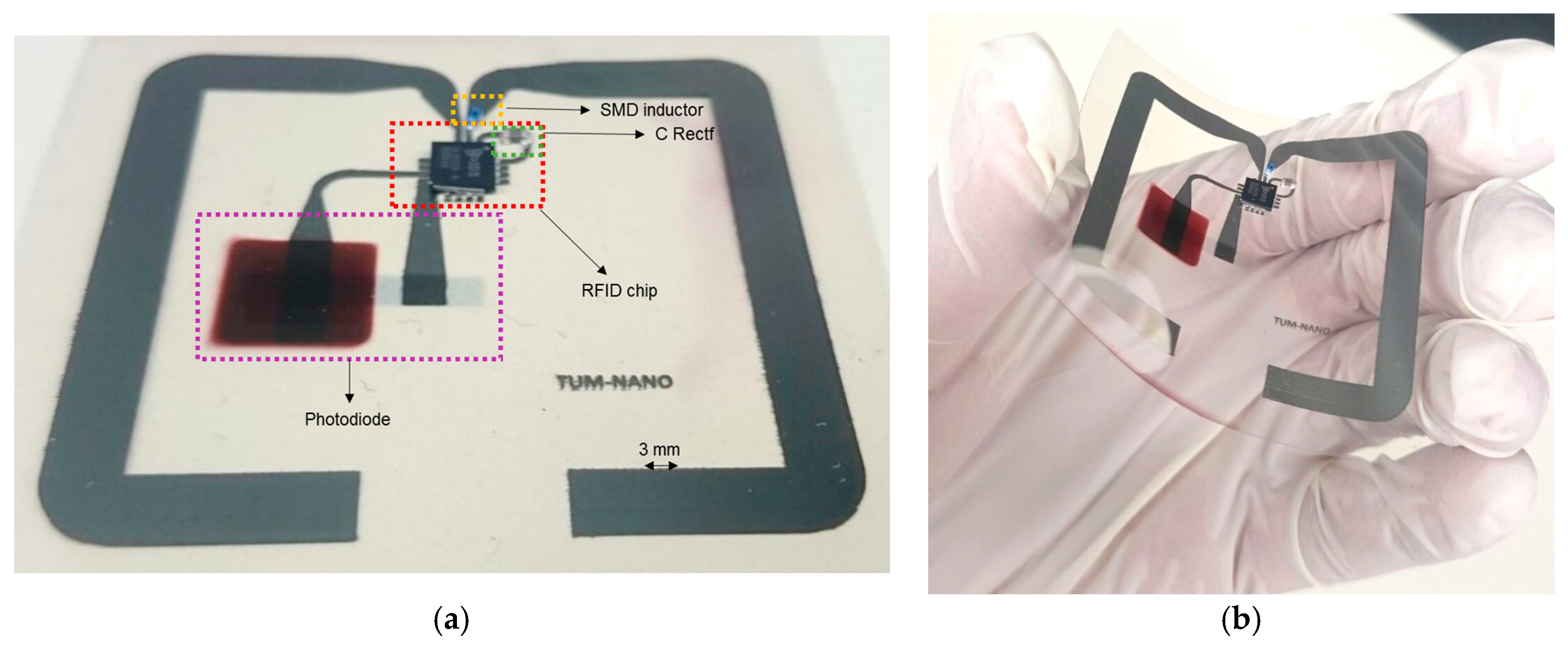
2.1. Tag Design
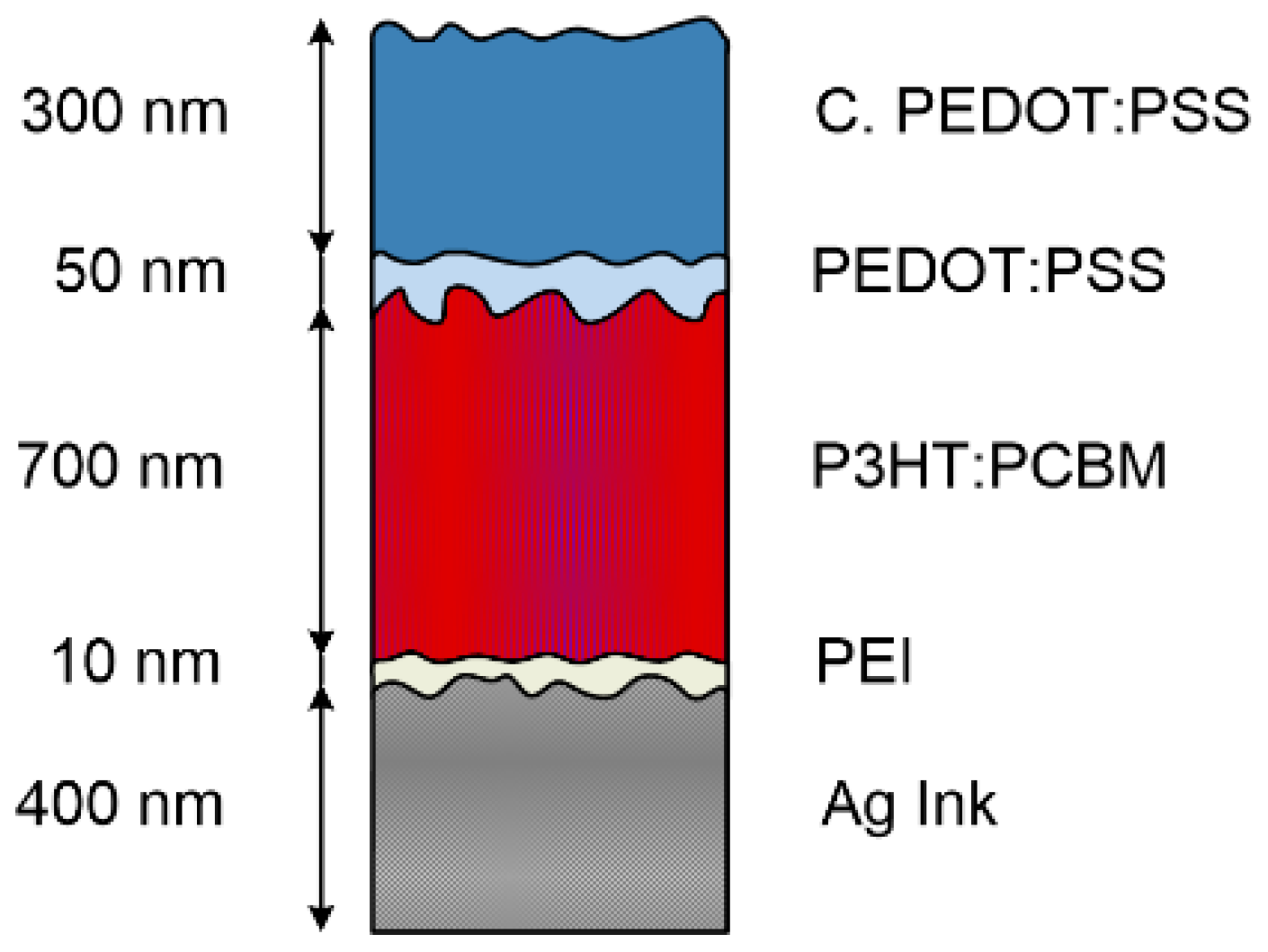
2.2. Materials
2.3. Fabrication Process
2.4. Characterization
3. Results and Discussion
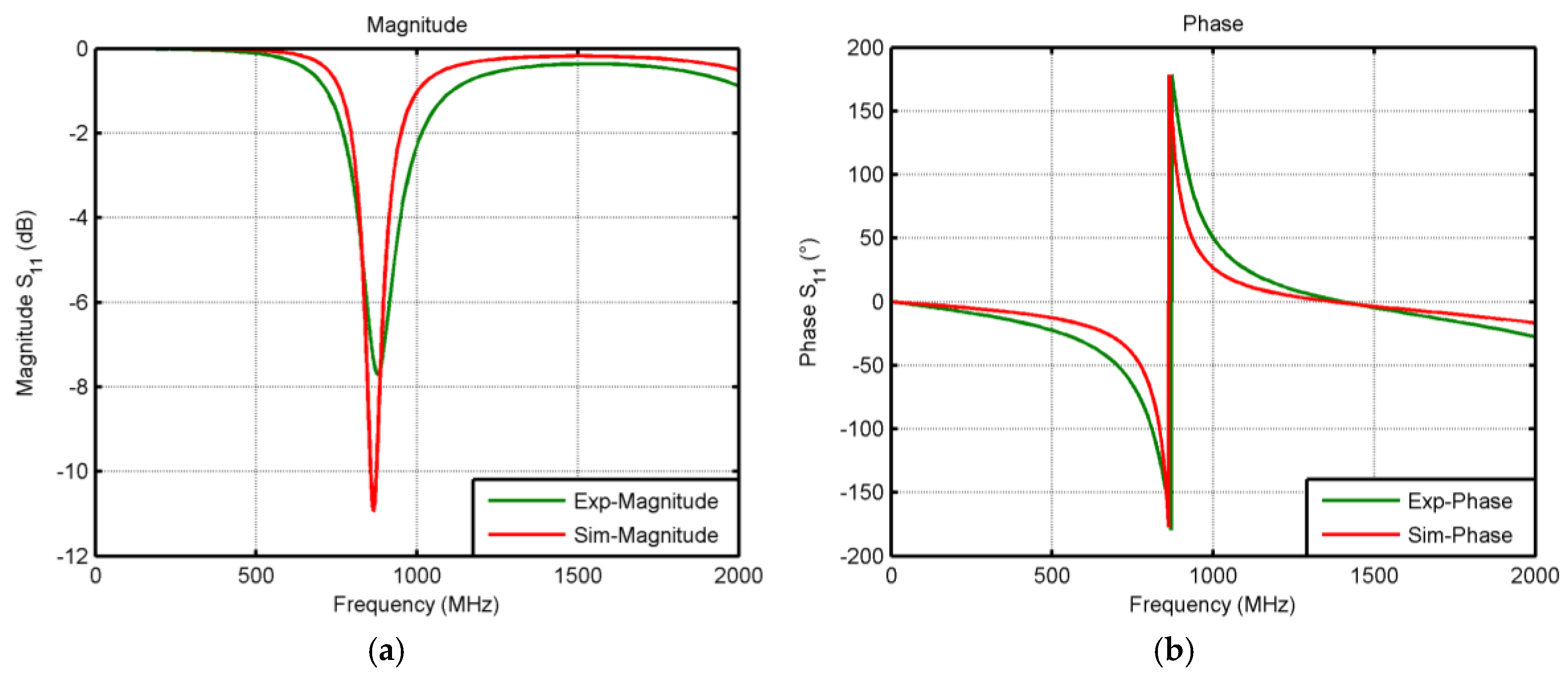
3.1. Antenna Performance
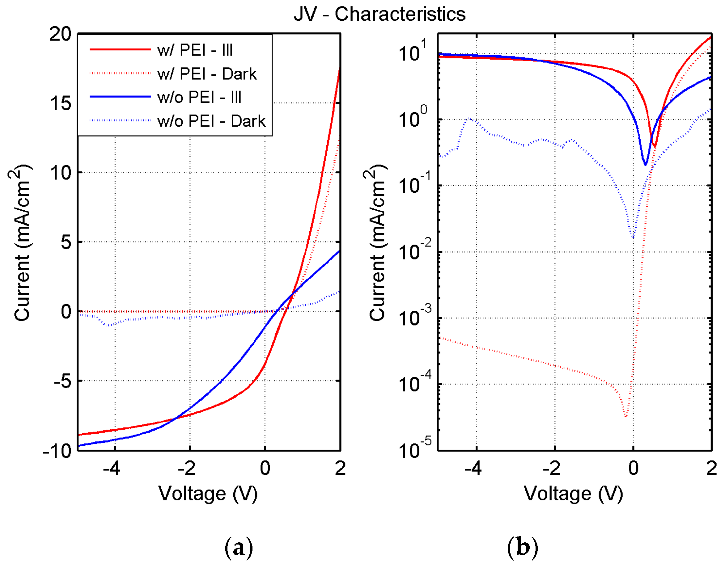
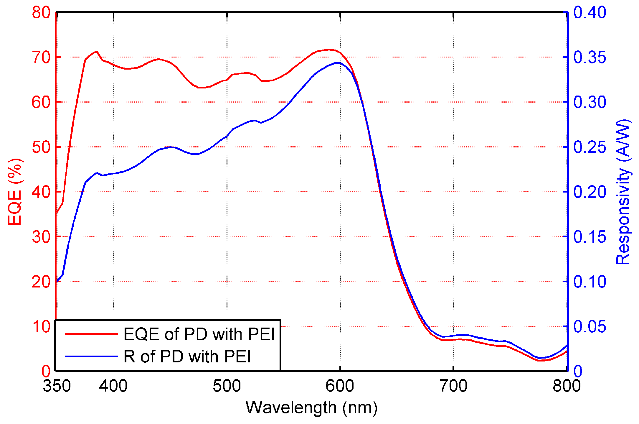
3.2. Photodiode Characterization
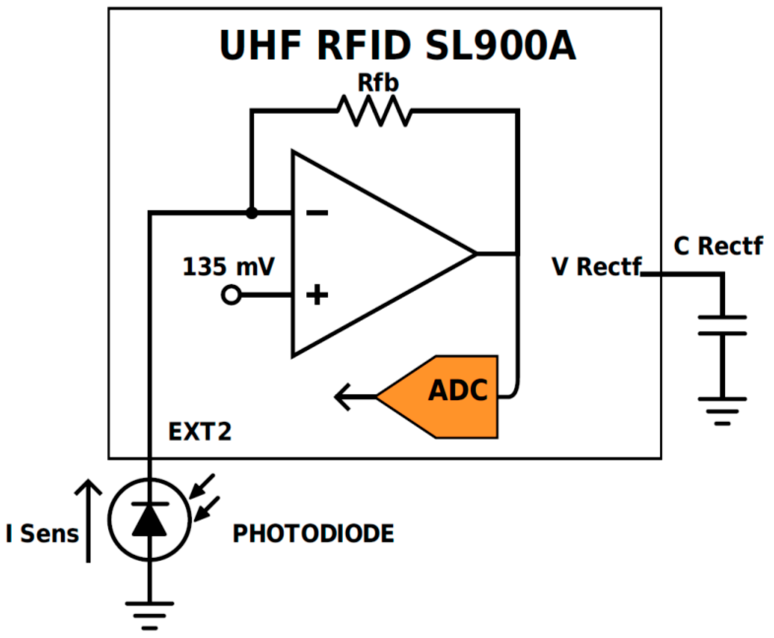
3.3. Tag Functioning
4. Conclusions
Acknowledgments
Author Contributions
Conflicts of Interest
References
- Chui, M.; Löffler, M.; Roberts, R. The internet of things. McKinsey Q. 2010, 2, 1–9. [Google Scholar]
- Verghese, K.; Lewis, H.; Lockrey, S.; Williams, H. Packaging’s Role in Minimizing Food Loss and Waste Across the Supply Chain. Packag. Technol. Sci. 2015, 28, 603–620. [Google Scholar] [CrossRef]
- Vanderroost, M.; Ragaert, P.; Devlieghere, F.; De Meulenaer, B. Intelligent food packaging: The next generation. Trends Food Sci. Technol. 2014, 39, 47–62. [Google Scholar] [CrossRef]
- Abad, E.; Palacio, F.; Nuin, M.; González de Zárate, A.; Juarros, A.; Gómez, J.; Marco, S. RFID smart tag for traceability and cold chain monitoring of foods: Demonstration in an intercontinental fresh fish logistic chain. J. Food Eng. 2009, 93, 394–399. [Google Scholar] [CrossRef]
- Kuswandi, B.; Wicaksono, Y.; Abdullah, A.; Heng, L.Y.; Ahmad, M. Smart packaging: sensors for monitoring of food quality and safety. Sens. Instrum. Food Qual. Saf. 2011, 5, 137–146. [Google Scholar] [CrossRef]
- Nicorescu, I.; Nguyen, B.; Chevalier, S.; Orange, N. Effects of pulsed light on the organoleptic properties and shelf-life extension of pork and salmon. Food Control 2014, 44, 138–145. [Google Scholar] [CrossRef]
- Gustavsson, J.; Cederberg, C.; Sonesson, U.; Van Otterdijk, R.; Meybeck, A. Global Food Losses and Food Waste; Food and Agriculture Organization of the United Nations: Rome, Italy, 2011. [Google Scholar]
- Nicola, S.; Fontana, E. Cultivation management on the farm influences postharvest quality and safety. In Proceedings of the International Conference on Quality Management of Fresh Cut Produce, Bangkok, Thailand, 6–8 August 2007; pp. 273–280.
- Nilsson, H.-E.; Unander, T.; Siden, J.; Andersson, H.; Manuilskiy, A.; Hummelgard, M.; Gulliksson, M. System integration of electronic functions in smart packaging applications. IEEE Trans. Compon. Packag. Manuf. Technol. 2012, 2, 1723–1734. [Google Scholar] [CrossRef]
- Suganuma, K. Introduction to Printed Electronics; Springer Science & Business Media: New York, NY, USA, 2014; Volume 74. [Google Scholar]
- Salmerón, J.F.; Molina-Lopez, F.; Rivadeneyra, A.; Quintero, A.V.; Capitán-Vallvey, L.F.; de Rooij, N.F.; Ozáez, J.B.; Briand, D.; Palma, A.J. Design and development of sensing RFID Tags on flexible foil compatible with EPC Gen 2. IEEE Sens. 2014, 14, 4361–4371. [Google Scholar] [CrossRef]
- Fernández-Salmerón, J.; Rivadeneyra, A.; Martínez-Martí, F.; Capitán-Vallvey, L.F.; Palma, A.J.; Carvajal, M.A. Passive UHF RFID Tag with Multiple Sensing Capabilities. Sensors 2015, 15, 26769–26782. [Google Scholar] [CrossRef] [PubMed]
- Unander, T.; Sidén, J.; Nilsson, H.-E. Designing of RFID-based sensor solution for packaging surveillance applications. IEEE Sens. J. 2011, 11, 3009–3018. [Google Scholar] [CrossRef]
- Gao, J.; Sidén, J.; Nilsson, H.; Gulliksson, M. Printed Humidity Sensor With Memory Functionality for Passive RFID Tags. IEEE Sens. J. 2013, 13, 1824–1834. [Google Scholar] [CrossRef]
- Salmerón, J.F.; Rivadeneyra, A.; Agudo, M.; Capitan-Vallvey, L.F.; Banqueri, J.; Carvajal, M.A.; Palma, A.J. Printed Single-chip UHF Passive Radiofrequency Identification Tags with Sensing Capability. Sens. Actuators A Phys. 2014, 220, 281–289. [Google Scholar] [CrossRef]
- Briand, D.; Molina-Lopez, F.; Quintero, A.V.; Mattana, G.; De Rooij, N.F. Printed sensors on smart RFID labels for logistics. In Proceedings of the 2012 IEEE 10th International New Circuits and Systems Conference (NEWCAS), Montreal, QC, Canada, 17–20 June 2012; pp. 449–452.
- Cho, N.; Song, S.-J.; Kim, S.; Kim, S.; Yoo, H.-J. A 5.1-μW UHF RFID tag chip integrated with sensors for wireless environmental monitoring. In Proceedings of the 31st European Solid-State Circuits Conference (ESSCIRC 2005), Grenoble, France, 12–16 September 2005; pp. 279–282.
- Yeager, D.J.; Sample, A.P.; Smith, J.R.; Smith, J.R. Wisp: A passively powered uhf rfid tag with sensing and computation. In RFID Handbook: Applications, Technology, Security, and Privacy; CRC Press: New York, NY, USA, 2008; pp. 261–278. [Google Scholar]
- Ag, A. Demo Kit for the SL900A Smart EPC Sensor Tag IC. Available online: http://www.ams.com/eng/Support/Design-Resources/Demoboards/UHF-RFID/UHF-Interface-and-Sensor-Tags/SL900A-DK-STQFN16 (accessed on 20 June 2016).
- Rao, K.S.; Nikitin, P.V.; Lam, S.F. Antenna design for UHF RFID tags: A review and a practical application. IEEE Trans. Antennas Propag. 2005, 53, 3870–3876. [Google Scholar] [CrossRef]
- Salmerón, J.F.; Molina-Lopez, F.; Briand, D.; Ruan, J.J.; Rivadeneyra, A.; Carvajal, M.A.; Capitán-Vallvey, L.; de Rooij, N.F.; Palma, A.J. Properties and Printability of Inkjet and Screen-Printed Silver Patterns for RFID Antennas. J. Electron. Mater. 2014, 43, 604–617. [Google Scholar] [CrossRef]
- Zhou, Y.; Fuentes-Hernandez, C.; Shim, J.; Meyer, J.; Giordano, A.J.; Li, H.; Winget, P.; Papadopoulos, T.; Cheun, H.; Kim, J. A universal method to produce low–work function electrodes for organic electronics. Science 2012, 336, 327–332. [Google Scholar] [CrossRef] [PubMed]
- Azzellino, G.; Grimoldi, A.; Binda, M.; Caironi, M.; Natali, D.; Sampietro, M. Fully Inkjet-Printed Organic Photodetectors with High Quantum Yield. Adv. Mater. 2013, 25, 6829–6833. [Google Scholar] [CrossRef] [PubMed]
- Falco, A.; Zaidi, A.; Lugli, P.; Abdellah, A. Spray deposition of Polyethylenimine thin films for the fabrication of fully-sprayed organic photodiodes. Org. Electron. 2015, 23, 186–192. [Google Scholar] [CrossRef]
- Falco, A.; Cinà, L.; Scarpa, G.; Lugli, P.; Abdellah, A. Fully-sprayed and flexible organic photodiodes with transparent carbon nanotube electrodes. ACS Appl. Mater. Interfaces 2014, 6, 10593–10601. [Google Scholar] [CrossRef] [PubMed]
- Schmidt, M.; Falco, A.; Loch, M.; Lugli, P.; Scarpa, G. Spray coated indium-tin-oxide-free organic photodiodes with PEDOT: PSS anodes. AIP Adv. 2014, 4, 107132. [Google Scholar] [CrossRef]
- Griffin, J.D.; Durgin, G.D. Complete link budgets for backscatter-radio and RFID systems. IEEE Antennas Propag. Mag. 2009, 51, 11–25. [Google Scholar] [CrossRef]
- Zahra’a, M.; AlSabbagh, H.M. Limitations of Forward and Return Links in UHF RFID with Passive Tags. Int. J. Eng. Trends Technol. 2013, 5, 238–242. [Google Scholar]
- Virtanen, J.; Virkki, J.; Elsherbeni, A.; Sydänheimo, L.; Ukkonen, L. A selective ink deposition method for the cost-performance optimization of inkjet-printed UHF RFID tag antennas. Int. J. Antennas Propag. 2012, 2012. [Google Scholar] [CrossRef]
- Leung, S.Y.; Lam, D.C. Performance of printed polymer-based RFID antenna on curvilinear surface. IEEE Trans. Electron. Packag. Manuf. 2007, 30, 200–205. [Google Scholar] [CrossRef]
- Sidén, J.; Jonsson, P.; Olsson, T.; Wang, G. Performance degradation of RFID system due to the distortion in RFID tag antenna. In Proceedings of the 11th International Conference on Microwave and Telecommunication Technology (CriMiCo 2001), Sevastopol, Crimea, Ukraine, 10–14 September 2001; pp. 371–373.
- Baeg, K.J.; Binda, M.; Natali, D.; Caironi, M.; Noh, Y.Y. Organic light detectors: Photodiodes and phototransistors. Adv. Mater. 2013, 25, 4267–4295. [Google Scholar] [CrossRef] [PubMed]
- Abdellah, A.; Fabel, B.; Lugli, P.; Scarpa, G. Spray deposition of organic semiconducting thin-films: Towards the fabrication of arbitrary shaped organic electronic devices. Org. Electron. 2010, 11, 1031–1038. [Google Scholar] [CrossRef]
- Sirringhaus, H.; Kawase, T.; Friend, R.; Shimoda, T.; Inbasekaran, M.; Wu, W.; Woo, E. High-resolution inkjet printing of all-polymer transistor circuits. Science 2000, 290, 2123–2126. [Google Scholar] [CrossRef] [PubMed]
- Liu, Z.; Su, Y.; Varahramyan, K. Inkjet-printed silver conductors using silver nitrate ink and their electrical contacts with conducting polymers. Thin Solid Films 2005, 478, 275–279. [Google Scholar] [CrossRef]
- Tedde, S.F.; Kern, J.; Sterzl, T.; Furst, J.; Lugli, P.; Hayden, O. Fully spray coated organic photodiodes. Nano Lett. 2009, 9, 980–983. [Google Scholar] [CrossRef] [PubMed]
- Pierre, A.; Deckman, I.; Lechêne, P.B.; Arias, A.C. High Detectivity All-Printed Organic Photodiodes. Adv. Mater. 2015, 27, 6411–6417. [Google Scholar] [CrossRef] [PubMed]


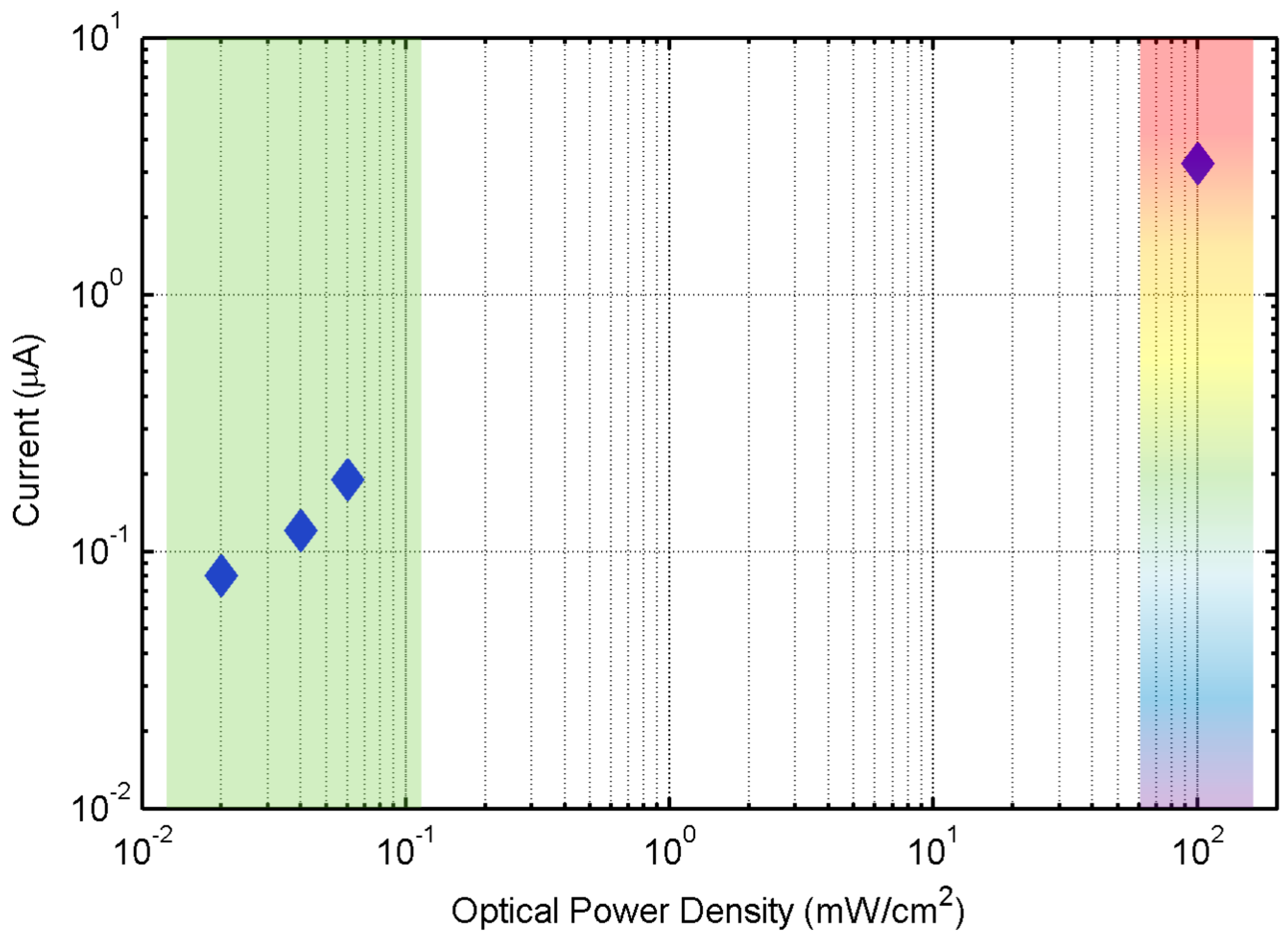
| Device/Configuration | Optical Power Density (mW/cm2) | ADC Count | Photocurrent (µA) |
|---|---|---|---|
| Sun simulator Rfb = 185 kΩ Vref1 = 0 mV Vref2 = 410 mV | 0 | 0 ± 0 | Below 1.5 |
| 100 | 810 ± 1 | 3.23 | |
| Monochromator (600 nm) Rfb= 3875 kΩ Vref1 = 0 mV Vref2 = 460 mV | 0.02 | 0 ± 0 | Below 0.8 |
| 0.04 | 256 ± 8 | 0.12 | |
| 0.08 | 884 ± 10 | 0.19 |
© 2017 by the authors. Licensee MDPI, Basel, Switzerland. This article is an open access article distributed under the terms and conditions of the Creative Commons Attribution (CC BY) license ( http://creativecommons.org/licenses/by/4.0/).
Share and Cite
Falco, A.; Salmerón, J.F.; Loghin, F.C.; Lugli, P.; Rivadeneyra, A. Fully Printed Flexible Single-Chip RFID Tag with Light Detection Capabilities. Sensors 2017, 17, 534. https://doi.org/10.3390/s17030534
Falco A, Salmerón JF, Loghin FC, Lugli P, Rivadeneyra A. Fully Printed Flexible Single-Chip RFID Tag with Light Detection Capabilities. Sensors. 2017; 17(3):534. https://doi.org/10.3390/s17030534
Chicago/Turabian StyleFalco, Aniello, Jose F. Salmerón, Florin C. Loghin, Paolo Lugli, and Almudena Rivadeneyra. 2017. "Fully Printed Flexible Single-Chip RFID Tag with Light Detection Capabilities" Sensors 17, no. 3: 534. https://doi.org/10.3390/s17030534