
Ultrasensitive Magnetic Nanoparticle Detector for Biosensor Applications


 ,
, 
Abstract
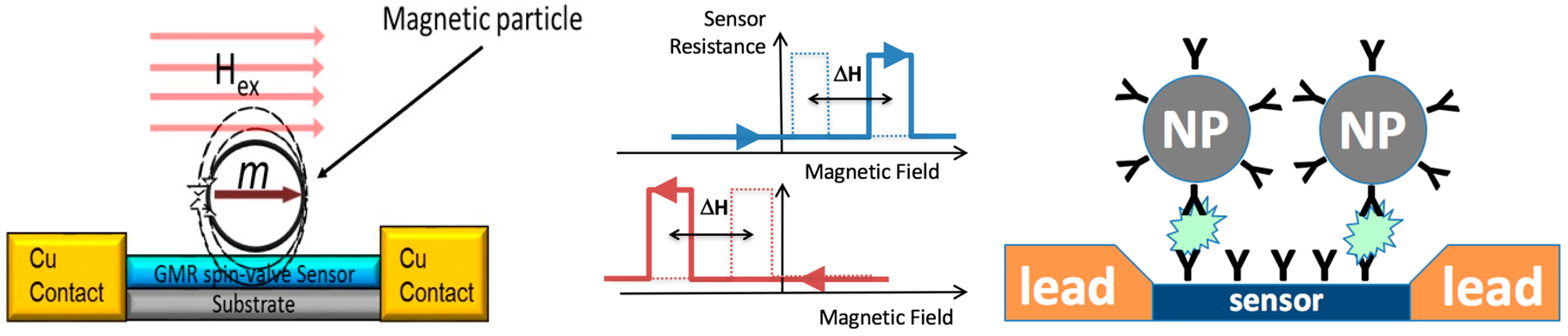
:1. Introduction
2. Materials and Methods
2.1. GMR Multilayer Deposition and Characterization
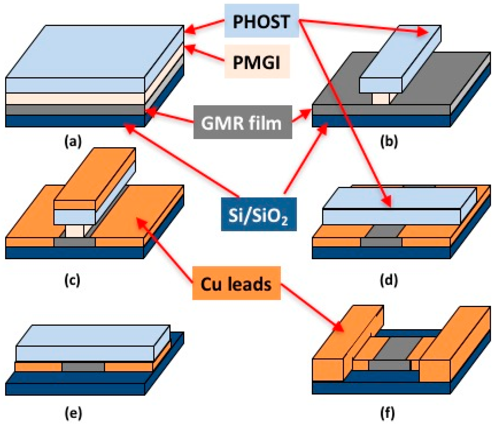
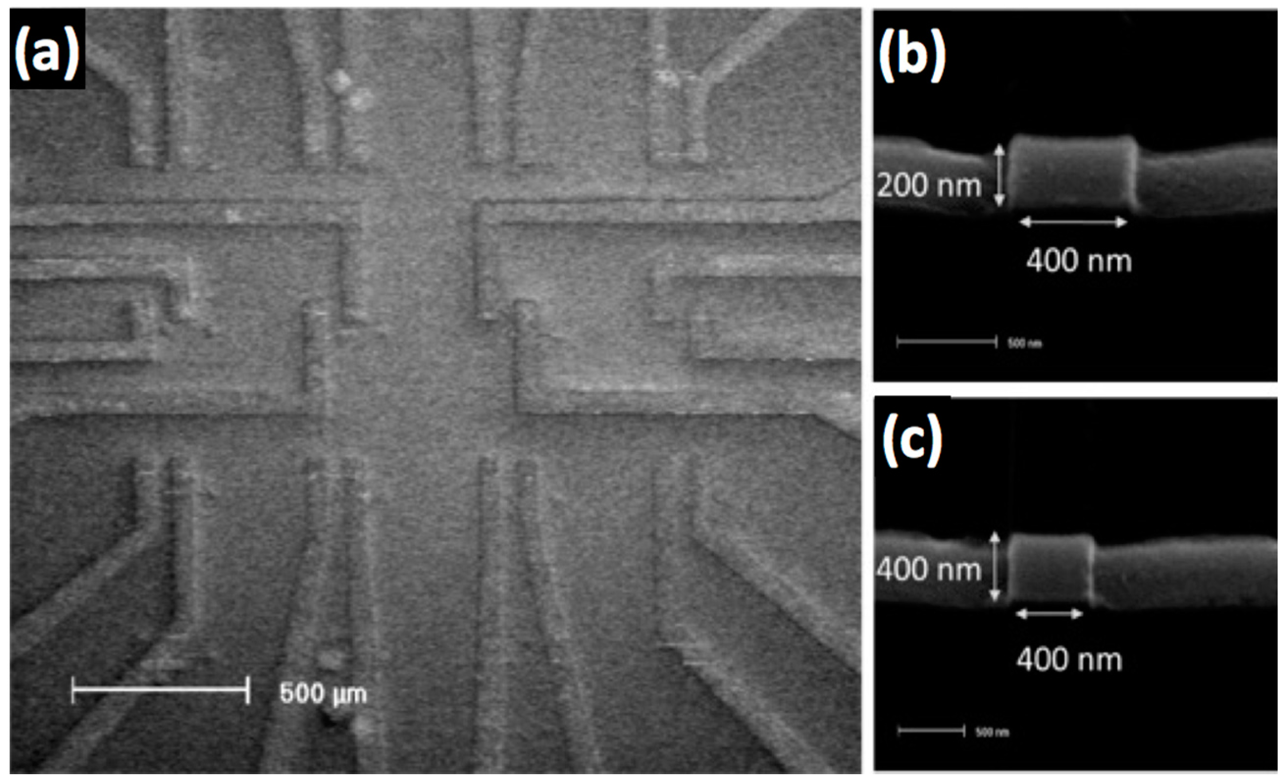
2.2. GMR Sensor Array Fabrication
2.3. Fe3O4 Magnetic Nanoparticle Synthesis
3. Results
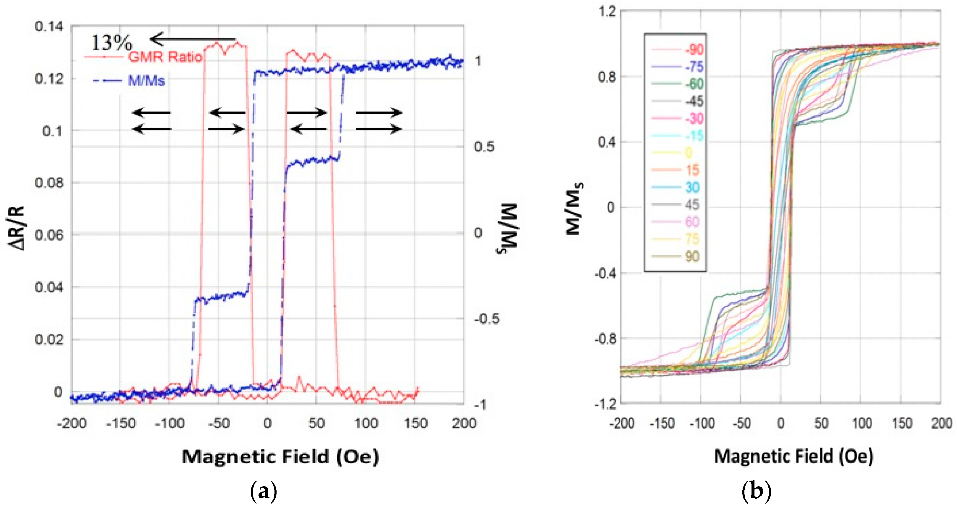
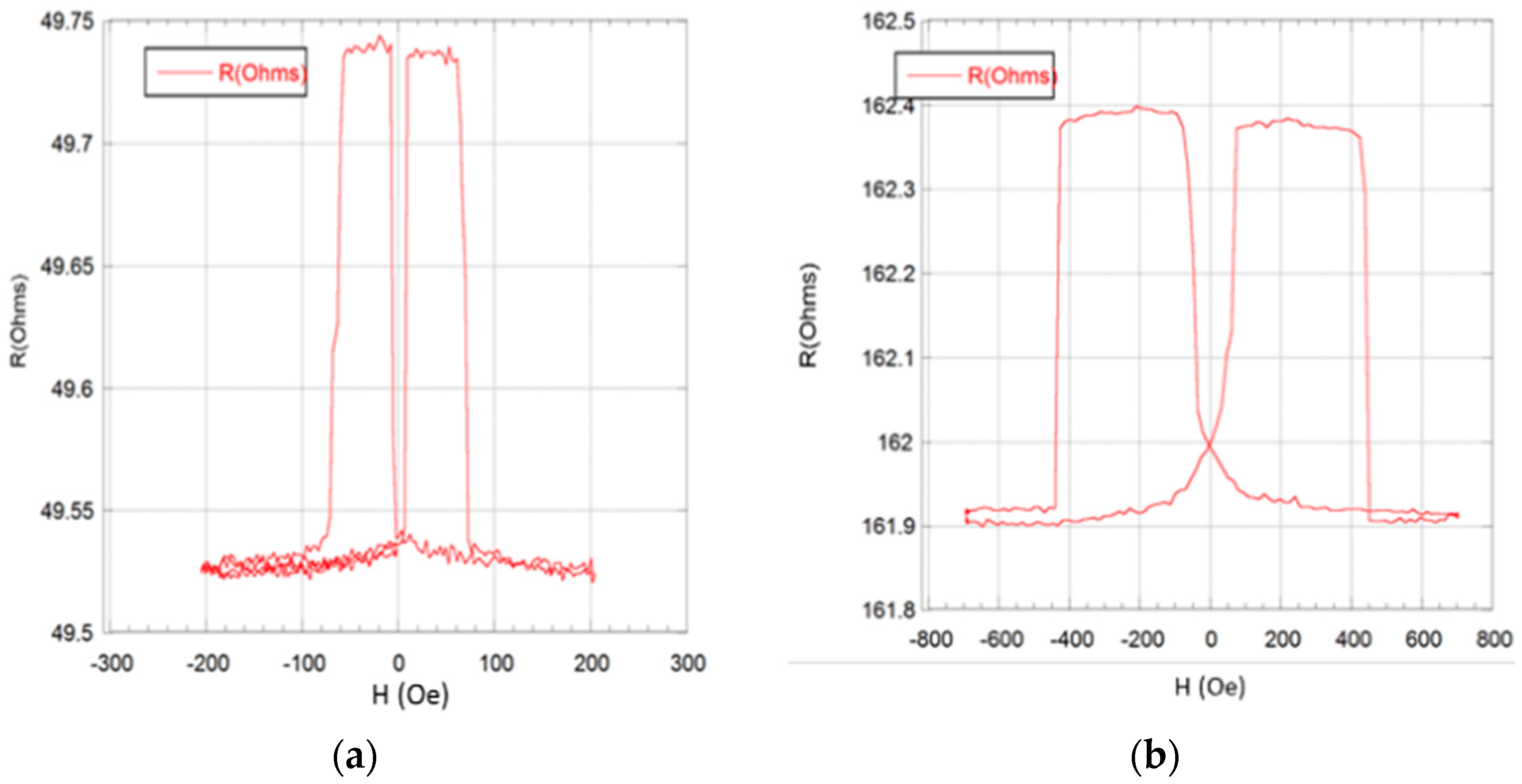
3.1. GMR Sensor Array Characterization
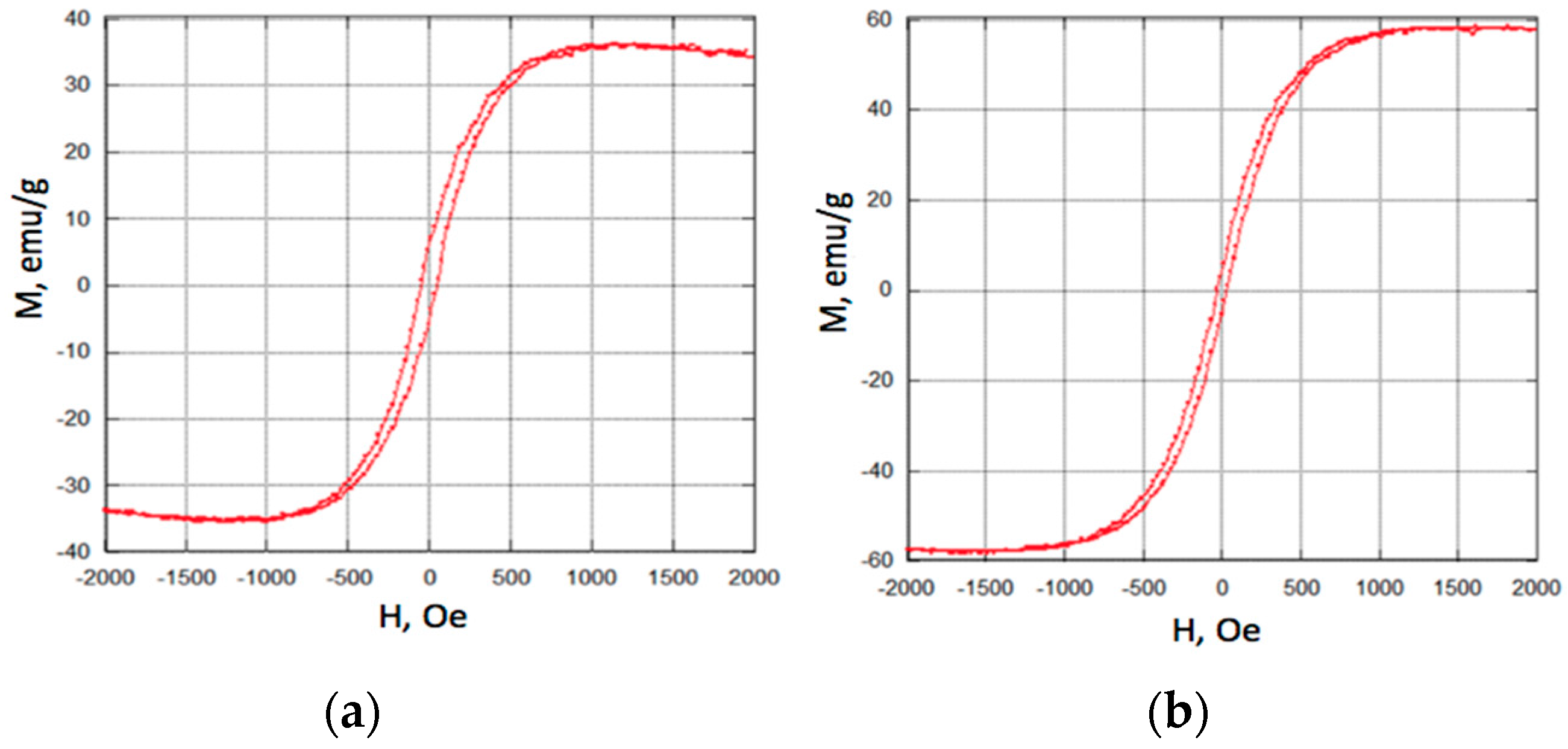
3.2. Fe3O4 Magnetic Nanoparticle Characterization
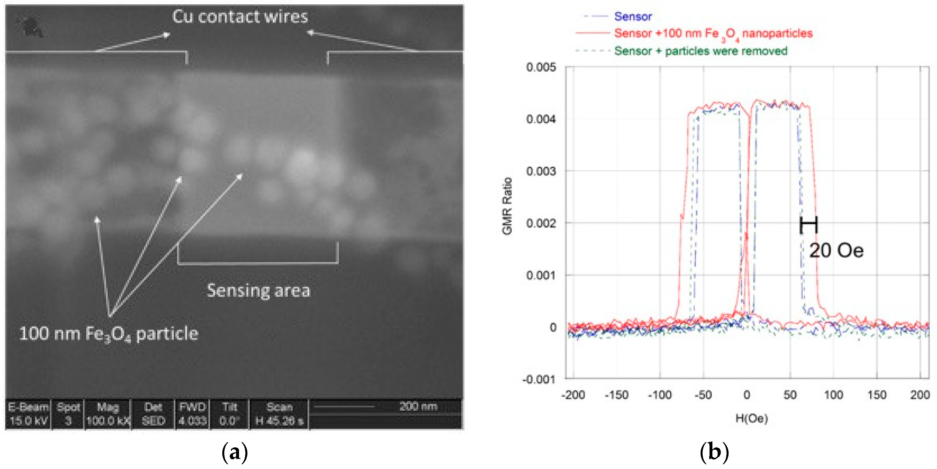
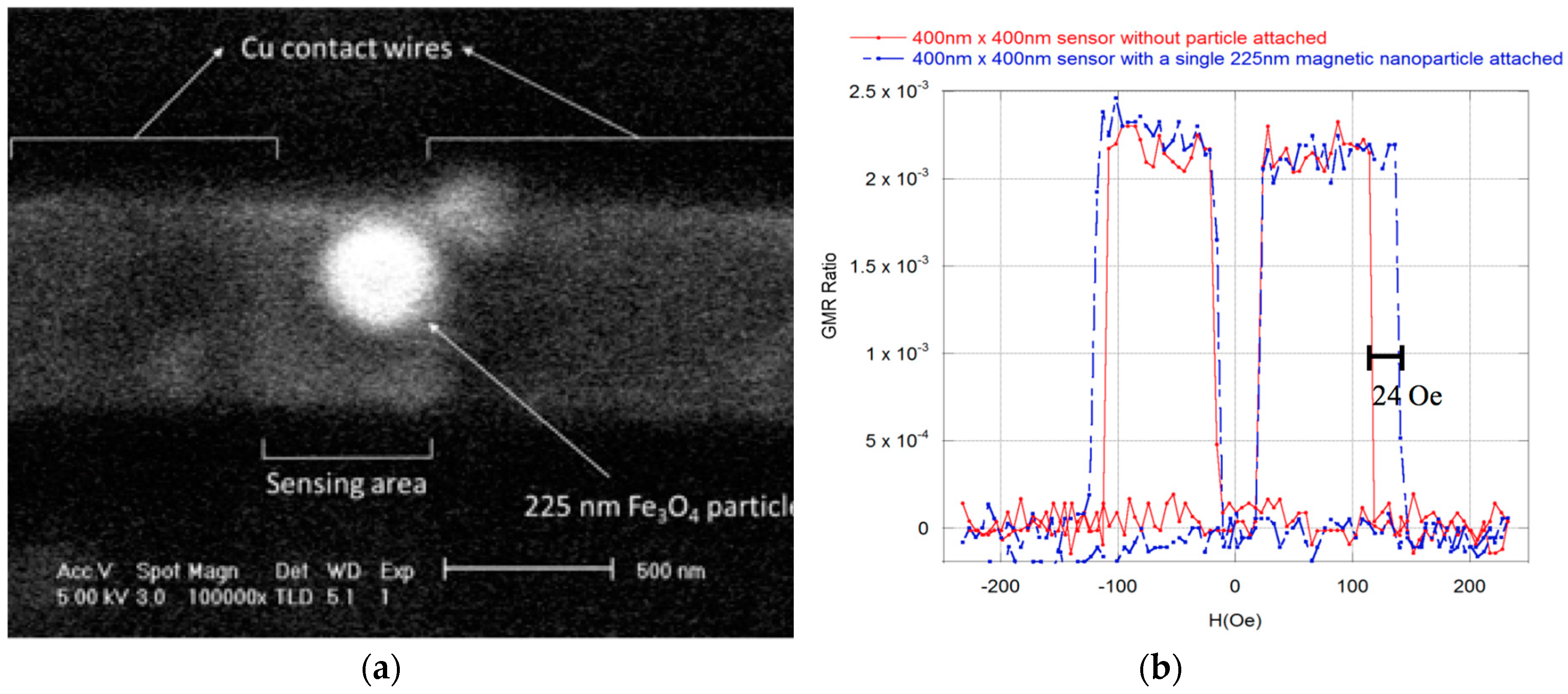
3.3. Application to Nanoparticle Detection
4. Discussion and Conclusions
Acknowledgments
Author Contributions
Conflicts of Interest
References
- Baibich, M.N.; Broto, J.M.; Fert, A.; Vandau, F.N.; Petroff, F.; Eitenne, P.; Creuzet, G.; Friederich, A.; Chazelas, J. Giant Magnetoresistance of (001)Fe/(001) Cr Magnetic Superlattices. Phys. Rev. Lett. 1988, 61, 2472–2475. [Google Scholar] [CrossRef] [PubMed]
- Binasch, G.; Grünberg, P.; Saurenbach, F.; Zinn, W. Enhanced magnetoresistance in layered magnetic structures with antiferromagnetic interlayer exchange. Phys. Rev. B Condens. Matter 1989, 39, 4828–4830. [Google Scholar] [CrossRef] [PubMed]
- Nozières, J.P.; Saporito, E.; Viala, B. Planar GMR head design for 50 Gbit/in2 recording. J. Magn. Magn. Mater. 2002, 242–245, 341–344. [Google Scholar] [CrossRef]
- Lazzari, J.P. Single pole, single turn, probe GMR head and micro-actuator for high-density perpendicular recording. J. Magn. Magn. Mater. 2001, 235, 362–367. [Google Scholar] [CrossRef]
- Nagasaka, K. CPP-GMR technology for magnetic read heads of future high-density recording systems. J. Magn. Magn. Mater. 2009, 321, 508–511. [Google Scholar] [CrossRef]
- Everitt, B.A.; Pohm, A.V.; Daughton, J.M. Size dependence of switching thresholds for pseudo spin valve MRAM cells. J. Appl. Phys. 1997, 81, 4020–4022. [Google Scholar] [CrossRef]
- Everitt, B.A.; Pohm, A.V. Pseudo spin valve magnetoresistive random access memory. J. Vac. Sci. Technol. A Vac. Surf. Films 1998, 16, 1794–1800. [Google Scholar] [CrossRef]
- Daughton, J.M. Magnetoresistive Memory Technology. Thin Solid Films 1992, 216, 162–168. [Google Scholar] [CrossRef]
- Baselt, D.R.; Lee, G.U.; Natesan, M.; Metzger, S.W.; Sheehan, P.E.; Colton, R.J. A biosensor based on magnetoresistance technology. Biosens. Bioelectron. 1998, 13, 731–739. [Google Scholar] [CrossRef]
- Graham, D.L.; Ferreira, H.A.; Freitas, P.P.; Cabral, J.M.S. High sensitivity detection of molecular recognition using magnetically labelled biomolecules and magnetoresistive sensors. Biosens. Bioelectron. 2003, 18, 483–488. [Google Scholar] [CrossRef]
- Xu, L.; Yu, H.; Akhras, M.S.; Han, S.-J.; Osterfeld, S.; White, R.L.; Pourmand, N.; Wang, S.X. Giant magnetoresistive biochip for DNA detection and HPV genotyping. Biosens. Bioelectron. 2008, 24, 99–103. [Google Scholar] [CrossRef] [PubMed]
- Wang, S.X.; Li, G. Advances in giant magnetoresistance biosensors with magnetic nanoparticle tags: Review and outlook. IEEE Trans. Magn. 2008, 44, 1687–1702. [Google Scholar] [CrossRef]
- Edelstein, R.L.; Tamanaha, C.R.; Sheehan, P.E.; Miller, M.M.; Baselt, D.R.; Whitman, L.J.; Colton, R.J. The BARC biosensor applied to the detection of biological warfare agents. Biosens. Bioelectron. 2000, 14, 805–813. [Google Scholar] [CrossRef]
- Ennen, I.; Kappe, D.; Rempel, T.; Glenske, C.; Hütten, A. Giant Magnetoresistance: Basic Concepts, Microstructure, Magnetic Interactions and Applications. Sensors 2016, 16, 904. [Google Scholar] [CrossRef] [PubMed]
- Rizzi, G.; Lee, J.-R.; Guldberg, P.; Dufva, M.; Wang, S.X.; Hansen, M.F. Denaturation strategies for detection of double stranded PCR products on GMR magnetic biosensor array. Biosens. Bioelectron. 2017, 93, 155–160. [Google Scholar] [CrossRef] [PubMed]
- Rizzi, G.; Østerberg, F.W.; Henriksen, A.D.; Dufva, M.; Hansen, M.F. On-chip magnetic bead-based DNA melting curve analysis using a magnetoresistive sensor. J. Magn. Magn. Mater. 2015, 380, 215–220. [Google Scholar] [CrossRef]
- Rizzi, G.; Dufva, M.; Hansen, M.F. Magnetoresistive sensors for measurements of DNA hybridization kinetics—Effect of TINA modifications. Sci. Rep. 2017, 7, 41940. [Google Scholar] [CrossRef] [PubMed]
- Rizzi, G.; Østerberg, F.W.; Dufva, M.; Hansen, M.F. Magnetoresistive sensor for real-time single nucleotide polymorphism genotyping. Biosens. Bioelectron. 2014, 52, 445–451. [Google Scholar] [CrossRef] [PubMed]
- Xu, J.; Li, Q.; Zong, W.; Zhang, Y.; Li, S. Ultra-wide detectable concentration range of GMR biosensors using Fe3O4 microspheres. J. Magn. Magn. Mater. 2016, 417, 25–29. [Google Scholar] [CrossRef]
- Srinivasan, B.; Li, Y.; Jing, Y.; Xu, Y.; Yao, X.; Xing, C.; Wang, J.P. A detection system based on giant magnetoresistive sensors and high-moment magnetic nanoparticles demonstrates zeptomole sensitivity: Potential for personalized medicine. Angew. Chem. Int. Ed. Engl. 2009, 48, 2764–2767. [Google Scholar] [CrossRef] [PubMed]
- Schotter, J.; Kamp, P.B.; Becker, A.; Puhler, A.; Reiss, G.; Bruckl, H. Comparison of a prototype magnetoresistive biosensor to standard fluorescent DNA detection. Biosens. Bioelectron. 2004, 19, 1149–1156. [Google Scholar] [CrossRef] [PubMed]
- Schotter, J.; Kamp, P.B.; Becker, A.; Puhler, A.; Brinkmann, D.; Schepper, W.; Bruckl, H.; Reiss, G. A biochip based on magnetoresistive sensors. IEEE Trans. Magn. 2002, 38, 3365–3367. [Google Scholar] [CrossRef]
- Lin, G.; Makarov, D.; Schmidt, O.G. Magnetic sensing platform technologies for biomedical applications. Lab Chip 2017, 17, 1884–1912. [Google Scholar] [CrossRef] [PubMed]
- Osterfeld, S.J.; Yu, H.; Gaster, R.S.; Caramuta, S.; Xu, L.; Han, S.J.; Hall, D.A.; Wilson, R.J.; Sun, S.H.; White, R.L.; et al. Multiplex protein assays based on real-time magnetic nanotag sensing. Proc. Natl. Acad. Sci. USA 2008, 105, 20637–20640. [Google Scholar] [CrossRef] [PubMed]
- Lenssen, K.-M.H.; Kuiper, A.E.T.; van den Broek, J.J.; van der Rijt, R.A.F.; van Loon, A. Sensor properties of a robust giant magnetoresistance material system at elevated temperatures. J. Appl. Phys. 2000, 87, 6665–6667. [Google Scholar] [CrossRef]
- Hardner, H.T.; Hurben, M.J.; Tabat, N. Noise and magnetic domain fluctuations in spin-valve GMR heads. IEEE Trans. Magn. 1999, 35, 2592–2594. [Google Scholar] [CrossRef]
- Kools, J.C.S. Exchange-biased spin-valves for magnetic storage. IEEE Trans. Magn. 1996, 32, 3165–3184. [Google Scholar] [CrossRef]
- Lederman, M. Performance of metallic antiferromagnets for use in spin-valve read sensors. IEEE Trans. Magn. 1999, 35, 794–799. [Google Scholar] [CrossRef]
- Goto, M.; Tange, H.; Kamimori, T. Thickness dependence of field induced uniaxial anisotropy in 80-permalloy films. J. Magn. Magn. Mater. 1986, 62, 251–255. [Google Scholar] [CrossRef]
- Sugita, Y.; Kawawake, Y.; Satomi, M.; Sakakima, H. /spl alpha/-Fe/sub 2/O/sub 3/ spin-valve using Co/Ru/Co synthetic antiferromagnet. In Proceedings of the IEEE International Magnetics Conference, Kyongju, Korea, 18–21 May 1999. [Google Scholar] [CrossRef]
- Leal, J.L.; Kryder, M.H. Spin valves exchange biased by Co/Ru/Co synthetic antiferromagnets. J. Appl. Phys. 1998, 83, 3720–3723. [Google Scholar] [CrossRef]
- Zhou, L.; Zhang, Z.; Wigen, P.E.; Ounadjela, K. Interlayer exchange coupling versus ferromagnetic layer thickness in asymmetric Co/Ru/Co trilayer films. J. Appl. Phys. 1994, 76, 7078–7080. [Google Scholar] [CrossRef]
- Guibert, J.C.; Chevalier, M.; Paniez, P.; Amblard, G. An improved bilayer PMGI (1) lithographic process. Microelectron. Eng. 1987, 6, 487–494. [Google Scholar] [CrossRef]
- De Meftahi, M.V.; Fréchet, J.M.J. Study of the compatibility of blends of polymers and copolymers containing styrene, 4-hydroxystyrene and 4-vinylpyridine. Polymer 1988, 29, 477–482. [Google Scholar] [CrossRef]
- Lee, S.M.; Frechet, J.M.; Willson, C.G. Photocrosslinking of Poly (4-hydroxystyrene) via Electrophilic Aromatic Substitution: Use of Polyfunctional Benzylic Alcohols in the Design of Chemically Amplified Resist Materials with Tunable Sensitivities. Macromolecules 1994, 27, 5154–5159. [Google Scholar] [CrossRef]
- Deng, H.; Li, X.L.; Peng, Q.; Wang, X.; Chen, J.P.; Li, Y.D. Monodisperse magnetic single-crystal ferrite microspheres. Angew. Chem. Int. Ed. 2005, 44, 2782–2785. [Google Scholar] [CrossRef] [PubMed]
- Sutens, B.; Swusten, T.; Zhong, K.; Jochum, J.; Van Bael, M.; Van der Eycken, E.; Brullot, E.; Bloemen, M.; Verbiest, T. Tunability of Size and Magnetic Moment of Iron Oxide Nanoparticles Synthesized by Forced Hydrolysis. Materials 2016, 9, 554. [Google Scholar] [CrossRef]
- Laurent, S.; Forge, D.; Port, M.; Roch, A.; Robic, C.; Vander Elst, L.; Muller, R.N. Magnetic iron oxide nanoparticles: Synthesis, stabilization, vectorization, physicochemical characterizations, and biological applications. Chem. Rev. 2008, 108, 2064–2110. [Google Scholar] [CrossRef] [PubMed]
- Woo, K.; Hong, J.; Choi, S.; Lee, H.-W.; Ahn, J.-P.; Kim, C.S.; Lee, S.W. Easy Synthesis and Magnetic Properties of Iron Oxide Nanoparticles. Chem. Mater. 2004, 16, 2814–2818. [Google Scholar] [CrossRef]
- Litvinov, J.; Wang, Y.-J.; George, J.; Chinwangso, P.; Brankovic, S.; Willson, R.C.; Litvinov, D. Development of Pinhole-Free Amorphous Aluminum Oxide Protective Layers for Biomedical Device Applications. Surf. Coat. Technol. 2013, 224, 101–108. [Google Scholar] [CrossRef] [PubMed]


© 2017 by the authors. Licensee MDPI, Basel, Switzerland. This article is an open access article distributed under the terms and conditions of the Creative Commons Attribution (CC BY) license (http://creativecommons.org/licenses/by/4.0/).
Share and Cite
Liang, Y.-C.; Chang, L.; Qiu, W.; Kolhatkar, A.G.; Vu, B.; Kourentzi, K.; Lee, T.R.; Zu, Y.; Willson, R.; Litvinov, D. Ultrasensitive Magnetic Nanoparticle Detector for Biosensor Applications. Sensors 2017, 17, 1296. https://doi.org/10.3390/s17061296
Liang Y-C, Chang L, Qiu W, Kolhatkar AG, Vu B, Kourentzi K, Lee TR, Zu Y, Willson R, Litvinov D. Ultrasensitive Magnetic Nanoparticle Detector for Biosensor Applications. Sensors. 2017; 17(6):1296. https://doi.org/10.3390/s17061296
Chicago/Turabian StyleLiang, Yu-Chi, Long Chang, Wenlan Qiu, Arati G. Kolhatkar, Binh Vu, Katerina Kourentzi, T. Randall Lee, Youli Zu, Richard Willson, and Dmitri Litvinov. 2017. "Ultrasensitive Magnetic Nanoparticle Detector for Biosensor Applications" Sensors 17, no. 6: 1296. https://doi.org/10.3390/s17061296