Analysis of the Optimum Gain of a High-Pass L-Matching Network for Rectennas


1
e-CAT Reaserch Group, Department of Electronic Engineering, Castelldefels School of Telecommunications and Aerospace Engineering, Universitat Politècnica de Catalunya, c/Esteve Terradas, 7, 08860 Castelldefels (Barcelona), Spain
2
CSC Research Group, Department of Signal Theory and Communications, Castelldefels School of Telecommunications and Aerospace Engineering, Universitat Politècnica de Catalunya, c/Esteve Terradas, 7, 08860 Castelldefels (Barcelona), Spain
*
Author to whom correspondence should be addressed.
Sensors 2017, 17(8), 1712; https://doi.org/10.3390/s17081712
Submission received: 8 April 2017
/
Revised: 29 June 2017
/
Accepted: 21 July 2017
/
Published: 25 July 2017
(This article belongs to the Special Issue Autonomous Sensors)
Abstract
:Rectennas, which mainly consist of an antenna, matching network, and rectifier, are used to harvest radiofrequency energy in order to power tiny sensor nodes, e.g., the nodes of the Internet of Things. This paper demonstrates for the first time, the existence of an optimum voltage gain for high-pass L-matching networks used in rectennas by deriving an analytical expression. The optimum gain is that which leads to maximum power efficiency of the rectenna. Here, apart from the L-matching network, a Schottky single-diode rectifier was used for the rectenna, which was optimized at 868 MHz for a power range from −30 dBm to −10 dBm. As the theoretical expression depends on parameters not very well-known a priori, an accurate search of the optimum gain for each power level was performed via simulations. Experimental results show remarkable power efficiencies ranging from 16% at −30 dBm to 55% at −10 dBm, which are for almost all the tested power levels the highest published in the literature for similar designs.
1. Introduction
Radio frequency (RF) energy harvesting has been widely proposed to power tiny devices such as RFID tags, autonomous sensors, or IoT (Internet of Things) nodes [1,2,3,4,5,6,7,8,9]. RF energy can be harvested either from dedicated sources, such as in the case of RFID devices, or from the RF energy already present in the ambient and coming from unintentional sources such as TV, FM radio, cellular, or WiFi emitters.
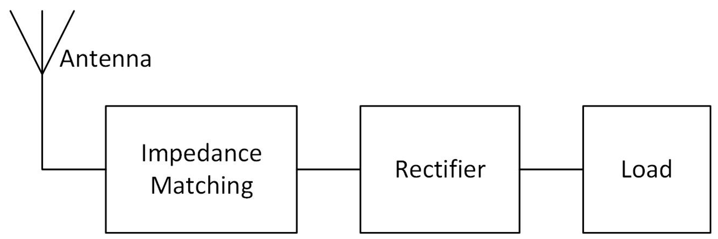
In order to harvest RF energy, a rectenna (rectifying antenna) is used. Figure 1 shows the block diagram of a conventional rectenna, consisting of an antenna, an impedance matching network and a rectifier. The rectifier provides a suitable DC voltage in order to power a load, e.g., an RFID tag or IoT node, and the matching network matches the output impedance of the antenna to the equivalent impedance at the input of the rectifier in order to transfer the available maximum power.
As the available power at the antenna decreases so does the generated voltage. Whenever this voltage is not high enough to properly bias the diodes of the rectifier, the power efficiency decreases severely. Several techniques have been proposed in order to increase the efficiency at low power levels. For example, in [1,2,10] dual-stage solutions were proposed, where each of the two implemented circuits was optimized for different ranges of input power. In [11], the size of the diode-connected MOS transistors was optimized. On the other hand, in order to reduce the voltage drop of the diodes, novel devices have been proposed such as MOS floating-gate devices [12], tunnel FETs [13], or MOS transistors with a new bulk connection [14]. Another widely used technique consists in using the matching network for boosting the voltage at the rectifier input [4,8,14,15,16,17,18,19,20,21,22,23,24,25,26]. Among them, one of the simplest and most widely used is the L-matching network, where the voltage gain is fixed by the resistance value of the load.
This paper demonstrates for the first time the existence of an optimum voltage gain for a high-pass L-matching network used in rectennas by deriving an analytical expression. The optimum gain is that which leads to maximum power efficiency of the rectenna. As the focus is on the matching network, a rectifier with a single series diode configuration was selected for simplicity. Input power levels in the range of −30 dBm to −10 dBm at the 868 MHz Short Range Devices (SRD) band were considered. At each power level, the value provided by the expression of the optimum gain was used as the initial point for an ensuing accurate search via simulations. The rectenna was later implemented and experimental results show remarkable power efficiencies compared with other works with similar designs found in the literature.
The paper is organized as follows: Section 2 presents a theoretical analysis of the rectenna where the analytical expression of the optimum voltage gain of the matching network is derived. Section 3 shows simulation results of the rectenna with the Keysight ADS software for obtaining the optimum gain and components of the matching network that will be used in the implementation of the circuit. In Section 4 the performance of the implemented rectenna is presented. Section 5 concludes the work and two appendices present supplemental material.
2. Theoretical Analysis of the Rectenna
This section presents the analysis of the rectenna with both an ideal (Section 2.1) and a lossy (Section 2.2) matching network. The optimum voltage gain of the matching network is derived in Section 2.2.
2.1. Rectenna with Ideal Matching Network
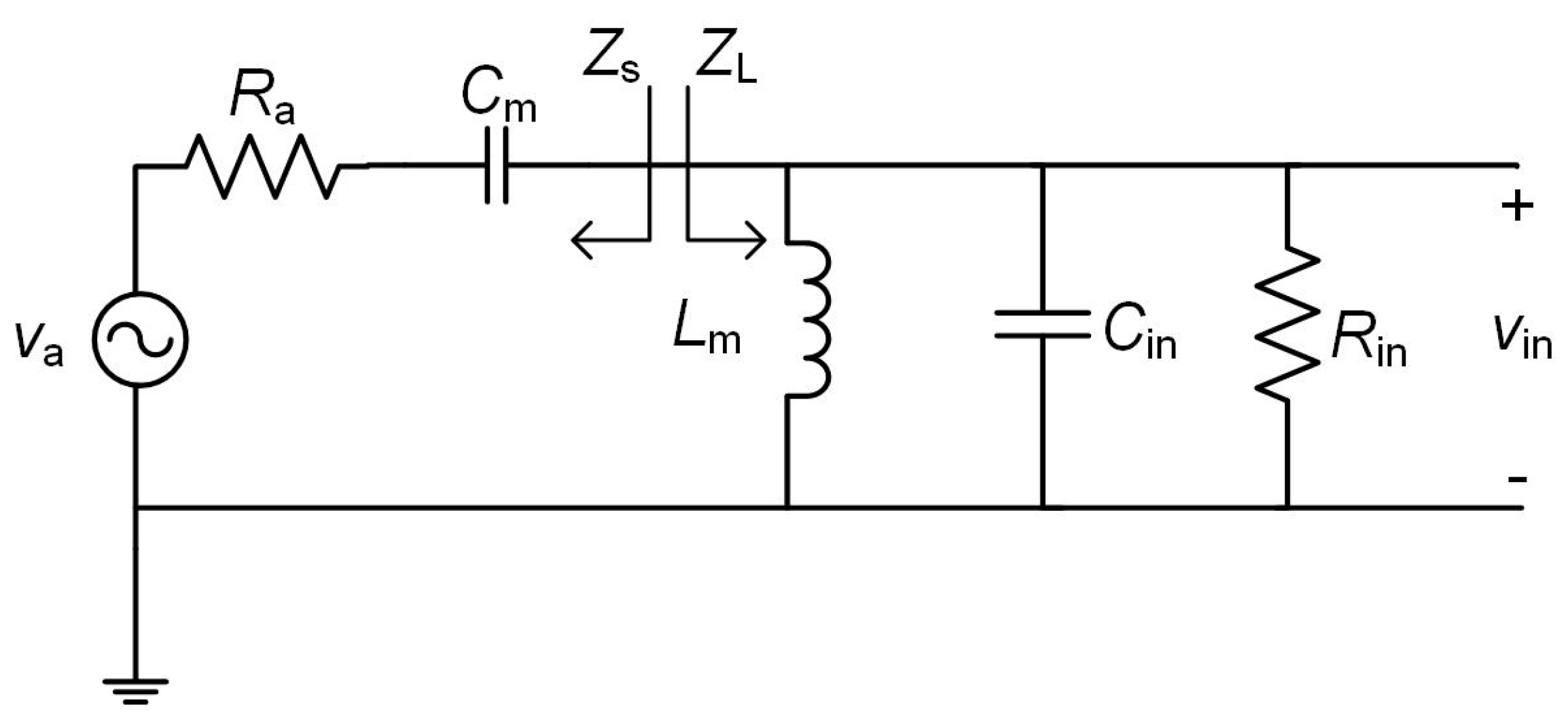
Figure 2 shows the circuit schematic of the proposed rectenna, which includes a high pass L-matching network (composed of a capacitor Cm and an inductor Lm), a half-wave rectifier and an output filtering capacitor (Co) and load (Ro). The antenna is modelled by a sinusoidal voltage source va with a series radiation resistance Ra. On the other hand, vin, Zin and Pin respectively are the voltage, impedance and power at the input of the rectifier, and Vo and Po respectively are the DC voltage and power at the load.
The voltage amplitude (or peak voltage) of va is given by [17]:
where Pav is the available power at the antenna. On the other hand, the overall power efficiency of the rectenna is defined as:
where the input efficiency is given by:
and the rectifier efficiency is:
being Vinp the amplitude voltage of vin and Vγ the threshold forward voltage of the diode (assumed constant here). Equation (4) is a simplistic approximation that neglects all the parasitic components and non idealities of the diode except Vγ.
In order to achieve a high value of ηin (ideally 1), Zin has to be matched to Ra. On the other hand, from Equation (4), lower values of Vγ and higher values of Vinp lead to a higher value of ηo. Thus, ηo can be increased, for example, by using Schottky diodes (low Vγ) and a matching network with a high voltage gain (high Vinp). In order to illustrate how the matching network provides this gain, the circuit of Figure 2 is transformed into the circuit of Figure 3, where Cin and Rin model Zin in Figure 2.
Cin is mainly due to the parasitic capacitance of the diode whenever Co is much larger, which is usually the case, and Rin, which models the power delivered to the rectifier input, is given by [27]:
In order to transfer the maximum power to the rectifier input (Pin = Pav and thus ηin = 1), it must be accomplished that , resulting in the following voltage gain of the matching network:
where Q is the quality factor of the circuit. Appendix A shows the resulting expressions for Cm and Lm as well graphs of these parameters in function of Gt.
As can be seen from Equation (6), Gt depends on the relationship between Rin and Ra, so the gain Gt can be made arbitrarily large by increasing Rin. Expression (6) can also be derived equating the power at the input of the matching network with that dissipated in Rin, assuming a lossless matching network [16]. Thus, an increase of Rin requires a square increase of vin (and thus of Gt) to keep power constant. On the other hand, Rin can be increased, from Equation (5), by increasing Ro. However, Ro is a priori fixed by the load to be powered, e.g., an IoT node. Fortunately, Ro can be arbitrarily and automatically changed by placing an additional impedance matching stage between the rectenna output and the load. Such stage, which is out of the scope of this work, is normally implemented by a maximum power point tracker, which has been extensively used in solar, thermal, and mechanical energy harvesters, but also in RF harvesters, such as in [28,29,30].
2.2. Rectenna with Lossy Matching Network: Optimum Voltage Gain
In the previous analysis, the losses of the matching network components have not been considered and thus will be taken into account next. As will be shown, their inclusion is significant and leads to the concept of optimum voltage gain of the matching network.
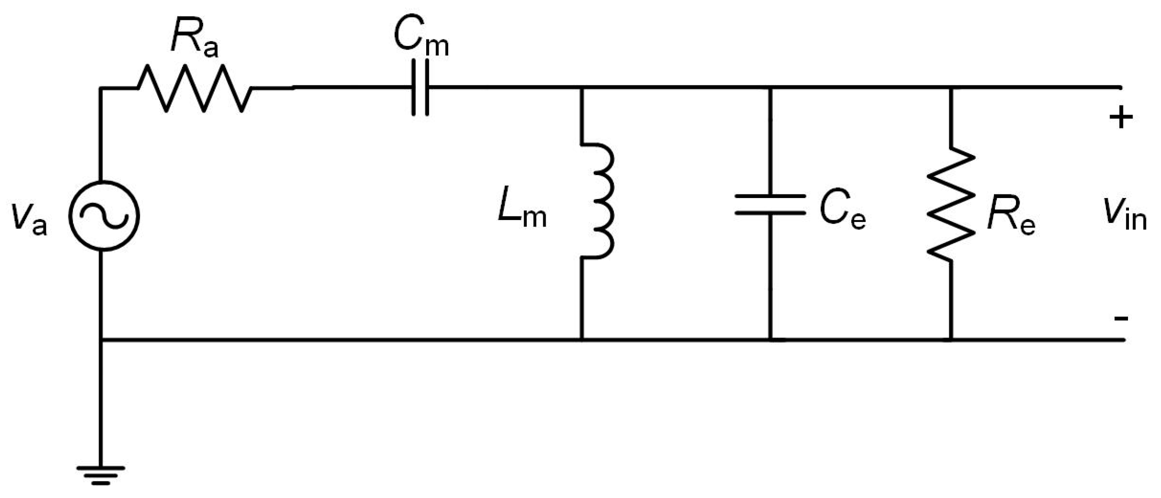
In general, the parasitic loss of capacitors is very small compared with that of inductors [16,31,32] and will be neglected in the analysis. Then, taking into account the inductor model of Appendix B, Figure 3 is transformed into Figure 4, where Lm ≈ and Cin and Rin have been substituted by Ce and Re. The resistance Re includes the parasitic losses (Rp) of the coil and is given by:
being:
and Ce includes the parasitic capacitance of the coil and is given by:
For the circuit of Figure 4, the gain of the matching lossy network is:
Now, even with a large value of Rin, Re and thus Gt will be limited by Rp. Further, at matching conditions [16]:
as some power will be dissipated at Rp. Therefore, large values of Rin (>>Rp and thus >>Re) decrease ηin without significantly increasing Gt and thus ηo. Contrariwise, low values of Rin (≪Rp and thus Rin ≈ Re) decrease Gt and thus ηo without significantly increasing ηin (≈1). So, a trade-off exists for achieving a maximum value of ηrect, which leads to an optimum Rin and Gt.
The optimum value of Gt can be found by expressing Equation (2) in function of Gt, equating its derivative to zero and finding the roots. First, operating from Equations (7) and (10), we obtain
and substituting this in Equation (11) we get:
On the other hand, using Equation (6) in Equation (4) we arrive at:
and thus from Equations (2), (13) and (14) we obtain:
Figure 5 shows a qualitative representation of Equations (13)–(15). As can be seen, ηin decreases and ηo increases with increasing values of Gt, leading to an optimum value of Gt (Gt,opt) that provides the maximum value of ηrect (ηmax).
The expression of Gt,opt can be reached by doing the derivative of Equation (15) with respect to Gt and equating to zero, thus arriving to the following third-degree equation:
In this case, only a single positive real root results, which can be approximated to:
The derivation and expression for Gt,opt has not previously reported in the literature. As can be seen, Gt,opt increases with increasing values of Rp and Vγ and with decreasing values of Vap. This can be also inferred from the above expressions and Figure 5. Effectively, from Equation (13), an increase of Rp (decrease of inductor losses) increases ηin, shifting upwards the corresponding curve in Figure 5 and thus to the right Gt,opt (higher value). At the same time, the value of ηmax will increase. On the other hand, from Equation (14), a higher value of Vγ or a lower value of Vap decrease ηo, shifting downwards the corresponding curve in Figure 5 and thus again to the right Gt,opt. In this case, though, ηmax will decrease. So, ηmax increases with increasing values of Rp and Vap and with decreasing values of Vγ.
In order to obtain Equation (17), the values of Vγ and Rp are required. However, Vγ depends on the current flowing through the diode, which depends on Pav but also on Gt. On the other hand, Rp depends on the specific commercial component of Lm, whose value, from Equation (A6), again depends on Gt. Therefore, it is not straightforward obtaining Gt,opt and it will be found here by simulations, as shown in Section 3. Anyhow, the above derivation demonstrates the existence of an optimum gain value, provides more insight on the optimum gain and rectenna efficiency, and from Equation (17) an initial guess can be used for the simulations.
3. Rectenna Simulation Analysis
Simulations of the rectenna of Figure 2 have been carried out using the Keysight ADS software. The Harmonic Balance Analysis was used in order to compute the steady state solutions. For the diode, a Schottky HSMS-2850 device (Avago Technologies, Sant Jose, CA, USA) was selected, as it presents a low voltage drop (Vγ ≈ 0.1 V @ 0.1 mA) and a low capacitance (Cjo = 0.18 pF). Input power levels from −30 dBm to −10 dBm in steps of 5 dBm were used at a frequency of 868 MHz. Commercial components from the vendor libraries for Cm (AVX, Fountain Inn, SC, USA) and Lm (Coilcraft, Cary, IL, USA) were also used. A layout was also included in the simulations and the Momentum simulator was executed in order to obtain the related S-parameters. The physical dimensions of the printed circuit board (PCB) were 30.75 mm long and 12.10 mm width. Figure 6 shows the layout of the PCB, with indications to the placement of the components. The parameters of a Rogers substrate (RO4003C, Rogers, Chandler, AZ, USA) were selected (εr = 3.55, tanδ = 0.0021, thickness = 1.524 mm).
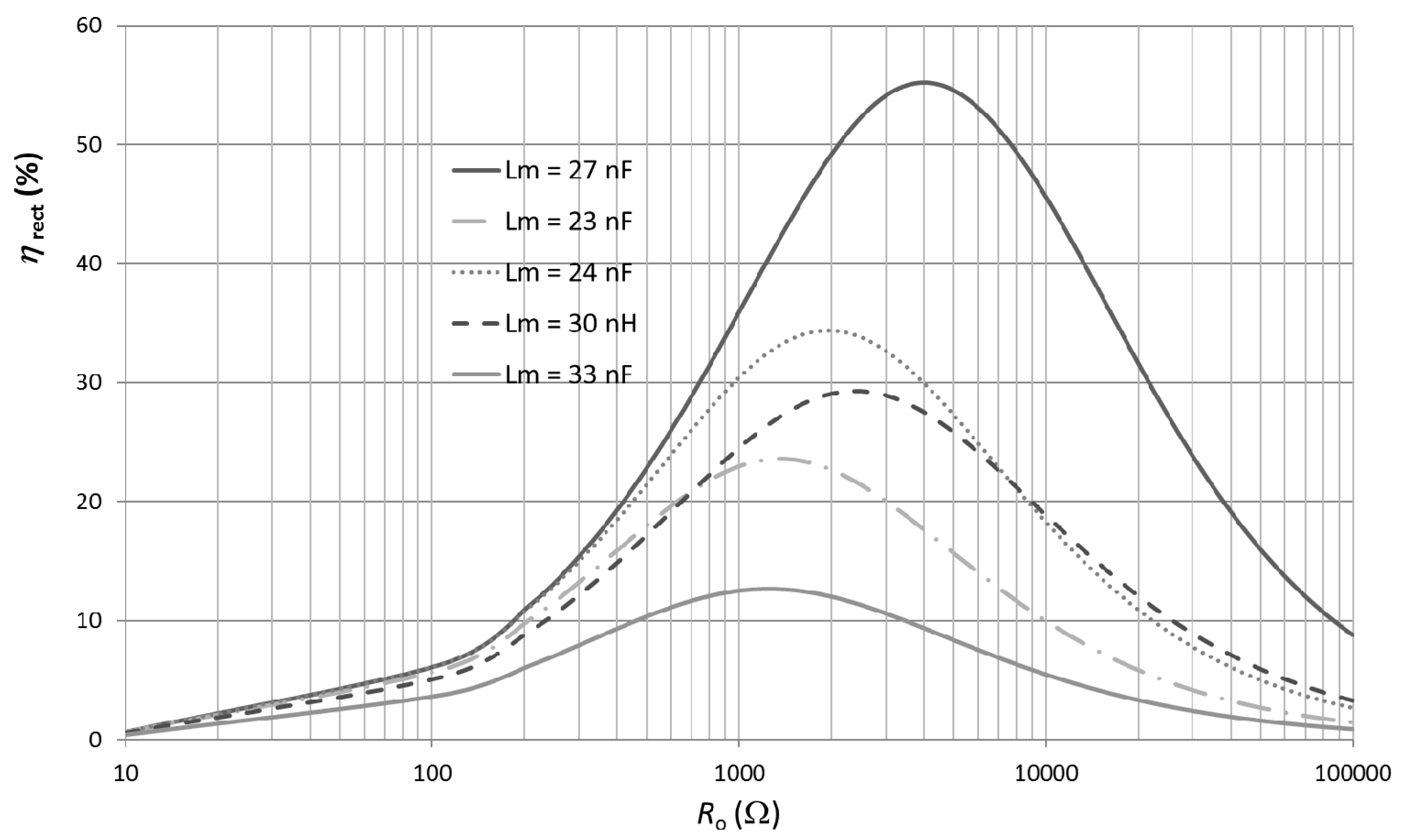
In order to find Gt,opt for each specific power level (Pav), the following procedure was followed. First, an initial value of Gt is calculated using Equation (17) with appropriate values of Vγ and Rp. From Equation (A5), the corresponding value of Cm is calculated and the component with the nearer commercial value is selected. Then, an appropriate component value of Lm is selected and a sweep of ηrect over Ro is performed. The procedure is repeated for several values of Lm until finding the curve with the maximum efficiency. In order to better illustrate the implemented procedure, Figure 7 shows the case for Pav = −10 dBm and Cm = 0.5 pF (Gt = 3.7). As can be seen, there is a maximum value of ηrect (around 55%) for Lm = 27 nH and Ro = 4 kΩ. These parameters values are saved and the whole procedure is repeated for different values of Cm (and thus of Gt). Figure 8 shows the attained maximum efficiencies for Pav = −10 dBm for each one of the selected values of Cm (or Gt). As can be seen, the maximum efficiency (ηmax) at −10 dBm was achieved for Gt = 3.7 (Cm = 0.5 pF, the case represented in Figure 7). Finally, the whole process is repeated for the different input power levels.
Table 1 summarizes the results of the simulations showing ηmax along with the optimal values of Gt, Cm, Lm, Ro, and Vo for each one of the selected power levels (Pav). As can be seen, the optimum value of Gt increases and ηmax decreases with a decreasing value of Pav and thus of Vap, which agrees with the discussion of Section 2.2. As a numerical example, the value of Gt,opt for −20 dBm is calculated using Equation (17). Taking the data of the 27 nH inductor from Appendix B, it can be found from Equation (8) that Rp is 12.6 kΩ. Then, assuming a value of Vγ = 0.1 V, Gt,opt = 3.94 results (Cm = 0.47 pF). The value of Cm shown in Table 1 (0.5 pF) is in fact the nearest commercial value available from the vendor library.
4. Experimental Results and Discussion
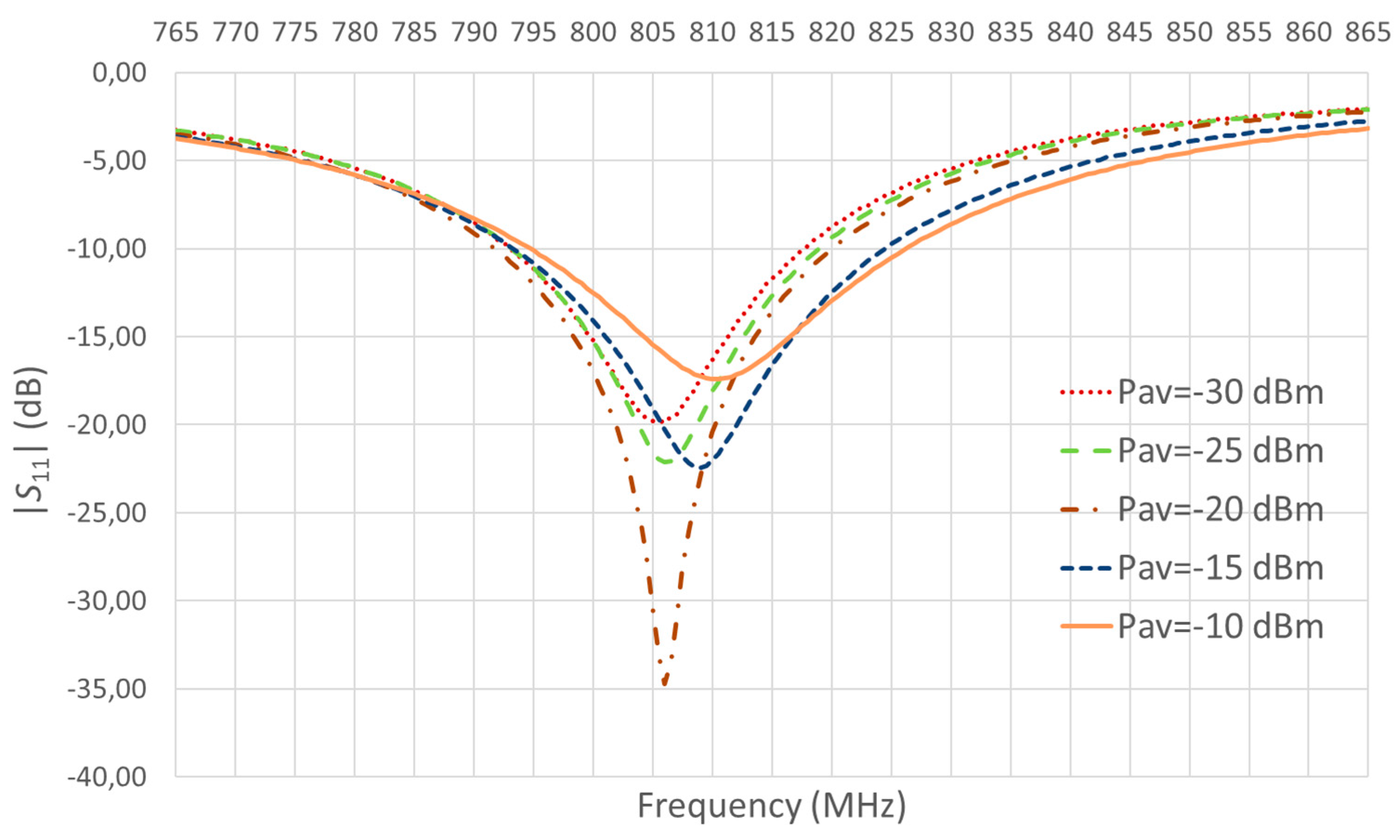
The PCB layout of Figure 6 was produced and Cm= 0.5 pF, Lm = 27 nH, and Co = 1 nF were used. The selected values of Cm and Lm lead to Gt = 3.7 and match that of Pav = −20 dBm, −15 dBm and −10 dBm in Table 1. In order to choose an appropriate frequency for the experimental tests, the input reflection coefficient S11 of the rectenna was measured for Pav from −30 dBm to −10 dBm in steps of 5 dBm using for Ro the corresponding values of Table 1. Results are shown in Figure 9.
As can be seen, there is a deviation of the frequencies at which the minimum value is achieved with respect to the theoretical frequency of 868 MHz used in the simulations. This is probably due to differences between the models of the components used in the simulations and their actual values. The tolerance of the network components and deviations of the parasitic capacitances of the inductor and diode can be the main cause. In addition, the capacitance of the diode is nonlinear with the diode voltage drop and thus with vin, which accounts for the frequency shift down as the power decreases [8]. On the other hand, Table 2 shows the values of the input impedance of the rectenna at a frequency of 814 MHz, which was the value selected for the rest of tests. As can be seen, values approach the value of Ra = 50 Ω and, from Figure 9, |S11| was lower than −10 dB at that frequency for all power levels.
An RF signal generator was used at the input of the harvester to emulate the antenna and to generate different values of Pav. Output power (Po) was measured by means of a Source Measurement Unit (SMU, B2901, Agilent, Santa Rosa, CA, USA). The frequency of the RF signal generator was set to 814 MHz, as previously stated, since it provided a relative high output power at all values of Pav. Anyhow, other nearby frequencies (with a difference of few units of megahertz, e.g., 810 MHz or 805 MHz) could have been chosen without significant changes in Po.
While measuring Po, the SMU fixed the output voltage (Vo) and this voltage was manually swept until the maximum value of Po (Po,max) was obtained. Maximum efficiency (ηmax) was estimated as Po,max divided by Pav. Then, the equivalent value of Ro was estimated from Vo and Po,max. This procedure was faster than using a trimmer for Ro and estimating Po from the measurements of Ro and Vo until Po,max was obtained. Table 3 shows the values of ηmax, Ro, and Vo. Values are similar to that of the simulations (Table 1). Efficiencies range from 15.7% at −30 dBm to 55.2% at −10 dBm.
Table 4 shows a comparative of the rectenna efficiency (in percentage) of this work with other papers using similar designs. Some of the values are imprecise as they were inferred from graphs. All of them use a matching network (in most cases an L-type) and the same model of diode (except in [10] that use an HSMS-282X model (Avago Technologies). The frequency was similar (in the range of 850 MHz to 950 MHz) except in [10] (2.45 GHz), [20] (434 MHz), and [33] (1.8 GHz). As can be seen, this work outperforms the results of the rest of papers except at −30 dBm, where [20] presents a higher efficiency. It is possible that the losses of the inductor used here, which limit the network gain and efficiency, are higher than those of the inductor used in [20] (details of the commercial inductor not provided).
5. Conclusions
This work has demonstrated the existence of an optimum voltage gain for L-matching networks used in rectennas by providing an analytical expression. The rectenna, which also includes a Schottky single-diode rectifier, has been optimized at 868 MHz for a power range from −30 dBm to −10 dBm. As not all the parameters of the expression are well known a priori, an accurate search of the gain has been performed by simulations. Furthermore, a prototype has been implemented with experimental results showing remarkable power efficiencies, ranging from 16% at −30 dBm to 55% at −10 dBm. These results are amongst the highest published in the literature for similar designs.
Acknowledgments
The authors wish to thank the technical staff of the EETAC for the fabrication of the PCB, J.M. González for their useful comments about ADS software, and the group Hipics of the UPC for providing the ADS software. This work was supported by the Spanish State Reasearch Agency (AEI) and by the European Regional Development Fund under Project TEC2016-76991-P.
Author Contributions
Manel Gasulla performed the theoretical analysis and jointly with Josep Jordana conceived and designed the experiments, and wrote the paper; Josep Jordana performed the simulations, implementation and experiments of the rectenna; Jordi Berenguer performed the measurements of the return loss and input impedance of the rectenna; Francesc-Josep Robert supported to Josep Jordana and Jordi Berenguer on the experiments and measurements.
Conflicts of Interest
The authors declare no conflict of interest. The founding sponsors had no role in the design of the study; in the collection, analyses, or interpretation of data; in the writing of the manuscript, and in the decision to publish the results.
Appendix A. Expressions for Cm and Lm and Corresponding Graphs
This appendix provides the expressions for Cm and Lm of the matching network along with graphs of these parameters.
In order to transfer the maximum power to the rectifier input, it must be accomplished that in Figure 3, where:
being ω the angular frequency. Operating, we obtain:
and the gain given by Equation (6). The parameters Lm and Cm can also be expressed in function of Gt and Q as:
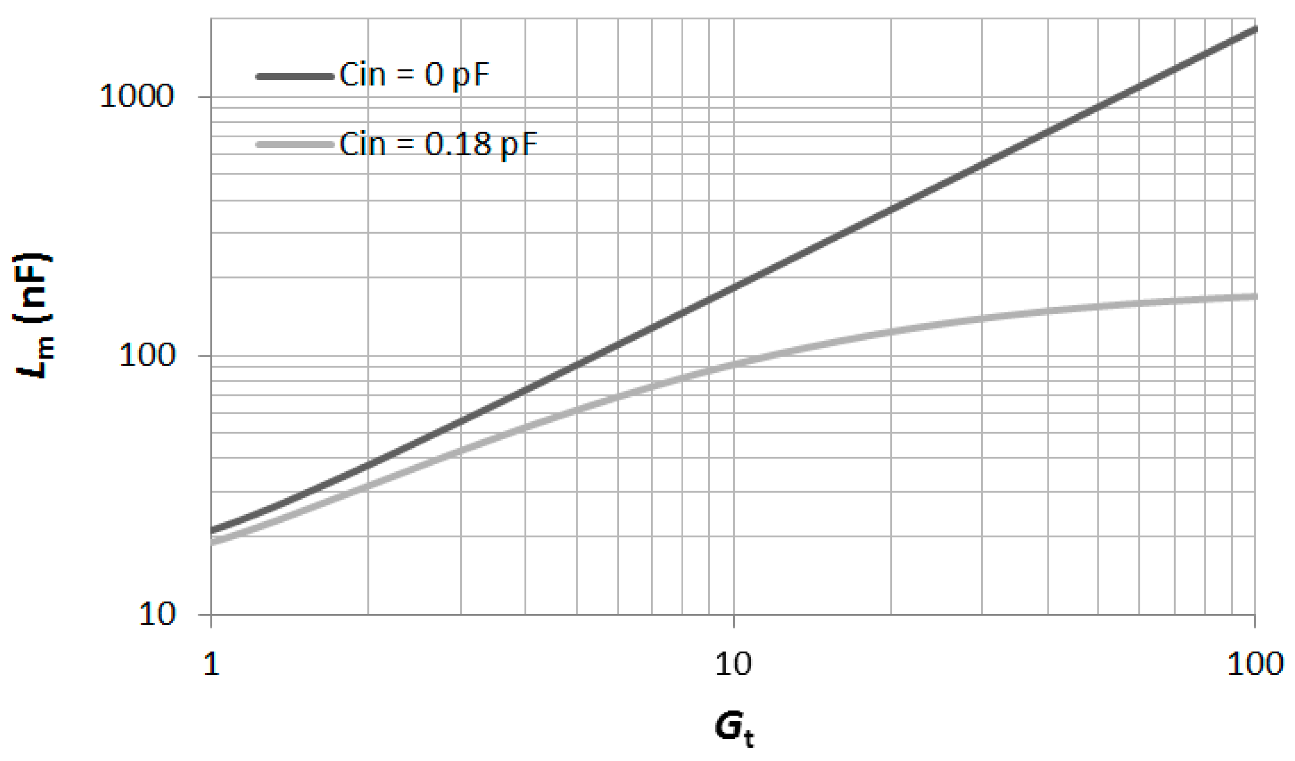
Figure A1 and Figure A2 show the values of Cm and Lm as a function of Gt for Ra = 50 Ω, respectively. As for the calculus of Lm, two different cases have been considered, Cin equal to 0 pF and to 0.18 pF. The value of 0.18 pF emulates the input capacitance of the selected diode (HSMS-2850) for the rectenna (Section 3 and Section 4). Cm is inversely proportional to Gt (strictly only for Gt >> 1) and Q. On the other hand, Lm is inversely proportional to Cm (so, proportional to Gt and Q) for Cin = 0 but for Cin = 0.18 pF saturates to with Gt (or Q) increasing (Cm decreasing).
Figure A1.
Cm values in function of Gt.
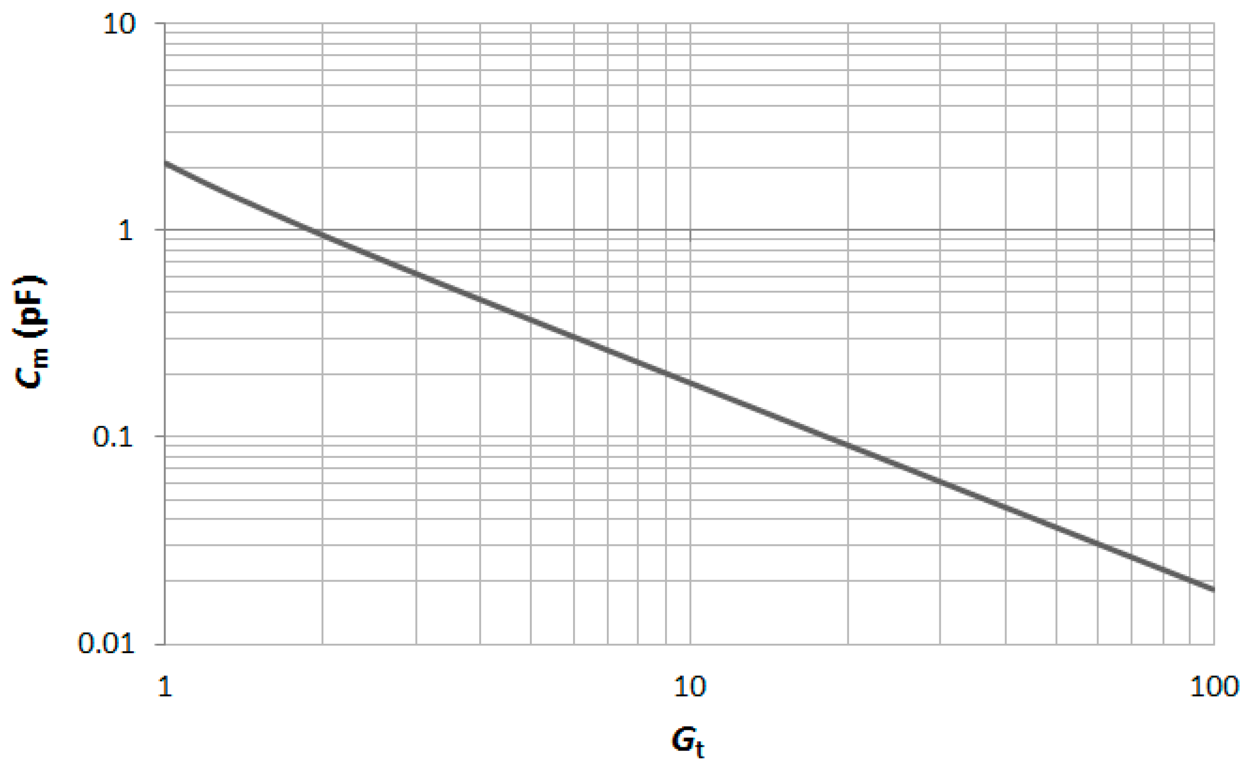
Figure A2.
Lm values in function of Gt for Cin = 0 pF and Cin = 0.18 pF.
Appendix B. Lumped Model of the Inductor Including Parasitic Effects
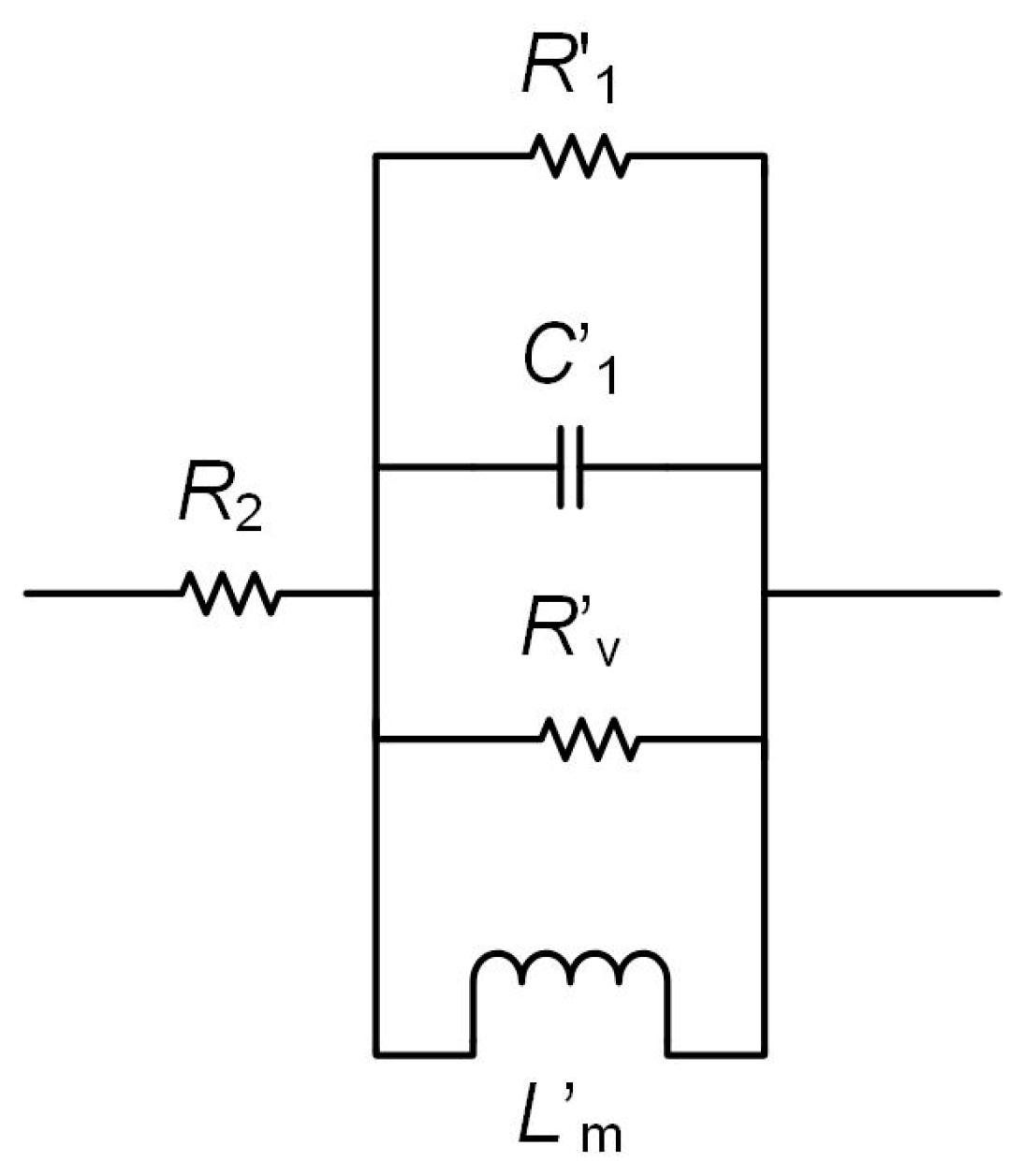
Figure A3 shows the lumped model of the Coilcraft RF surface mount inductor used in the implementation of the circuit of Figure 2. The value of the frequency-dependent variable resistor Rv relates to the skin effect and is calculated from , where f is the operation frequency and k’ is a constant that depends on the nominal value of the inductance.
Figure A3.
Equivalent lumped element model of the inductor.
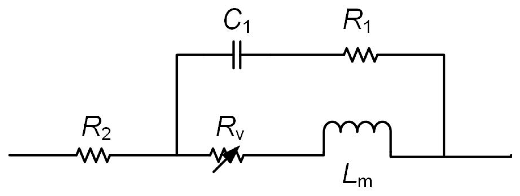
Using the series to parallel equivalent circuit transformation for the two branches of Figure A3 the equivalent circuit of Figure A4 results.
Figure A4.
Parallel equivalent circuit of the inductor of Figure A3.
Figure A4.
Parallel equivalent circuit of the inductor of Figure A3.

The value of the components of the circuit of Figure A4 respect to those of the circuit of Figure A3 are given by the following expressions:
The model of Figure A4 is substituted in the circuit of Figure 3, resulting in the circuit of Figure 4, where the value of R2 has been neglected as it usually is very small. As an example, the 27 nH inductor used in the implemented matching network (Section 4) has the following parameters: R1 = 17 Ω, R2 = 30 mΩ, C1 = 49 fF, Lm = 27 nH, k’ = 5.75 × 10⁻⁵. At 868 MHz the value of the parallel components of Figure A4 are: , , , .
References
- Nintanavongsa, P.; Muncuk, U.; Lewis, D.R.; Chowdhury, K.R. Design Optimization and Implementation for RF Energy Harvesting Circuits. IEEE J. Emerg. Sel. Top. Circuits Syst. 2012, 2, 24–33. [Google Scholar] [CrossRef]
- Di Marco, P.; Stornelli, V.; Ferri, G.; Pantoli, L.; Leoni, A. Dual band harvester architecture for autonomous remote sensors. Sens. Actuators A Phys. 2016, 247, 598–603. [Google Scholar] [CrossRef]
- Shaker, G.; Chen, R.; Milligan, B.; Qu, T. Ambient electromagnetic energy harvesting system for on-body sensors. Electron. Lett. 2016, 52, 1834–1836. [Google Scholar] [CrossRef]
- Attaran, A.; Rashidzadeh, R.; Muscedere, R. Chipless RFID tag using RF MEMS switch. Electron. Lett. 2014, 50, 1720–1722. [Google Scholar] [CrossRef]
- Talla, V.; Kellogg, B.; Ransford, B.; Naderiparizi, S.; Gollakota, S.; Smith, J.R. Powering the Next Billion Devices with Wi-Fi. Commun. ACM 2015, 60, 83–92. [Google Scholar] [CrossRef]
- Pinuela, M.; Mitcheson, P.D.; Lucyszyn, S. Ambient RF Energy Harvesting in Urban and Semi-Urban Environments. IEEE Trans. Microw. Theory Tech. 2013, 61, 2715–2726. [Google Scholar] [CrossRef]
- Kaushik, K.; Mishra, D.; De, S.; Chowdhury, K.R.; Heinzelman, W. Low-Cost Wake-Up Receiver for RF Energy Harvesting Wireless Sensor Networks. IEEE Sens. J. 2016, 16, 6270–6278. [Google Scholar] [CrossRef]
- Singh, G.; Ponnaganti, R.; Prabhakar, T.V.; Vinoy, K.J. A tuned rectifier for RF energy harvesting from ambient radiations. AEU Int. J. Electron. Commun. 2013, 67, 564–569. [Google Scholar] [CrossRef]
- Sample, A.; Smith, J.R. Experimental results with two wireless power transfer systems. In Proceedings of the 2009 IEEE Radio and Wireless Symposium, San Diego, CA, USA, 18–22 January 2009; IEEE: New York, NY, USA, 2009; pp. 16–18. [Google Scholar]
- Mirzavand, F.; Nayyeri, V.; Soleimani, M.; Mirzavand, R. Efficiency improvement of WPT system using inexpensive auto-adaptive impedance matching. Electron. Lett. 2016, 52, 2055–2057. [Google Scholar] [CrossRef]
- Yi, J.; Ki, W.-H.; Tsui, C.-Y. Analysis and Design Strategy of UHF Micro-Power CMOS Rectifiers for Micro-Sensor and RFID Applications. IEEE Trans. Circuits Syst. I Regul. Pap. 2007, 54, 153–166. [Google Scholar] [CrossRef]
- Le, T.; Mayaram, K.; Fiez, T. Efficient Far-Field Radio Frequency Energy Harvesting for Passively Powered Sensor Networks. IEEE J. Solid-State Circuits 2008, 43, 1287–1302. [Google Scholar] [CrossRef]
- Liu, H.; Li, X.; Vaddi, R.; Ma, K.; Datta, S.; Narayanan, V. Tunnel FET RF Rectifier Design for Energy Harvesting Applications. IEEE J. Emerg. Sel. Top. Circuits Syst. 2014, 4, 400–411. [Google Scholar] [CrossRef]
- Shokrani, M.R.; Khoddam, M.; Hamidon, M.N.B.; Kamsani, N.A.; Rokhani, F.Z.; Shafie, S. Bin An RF Energy Harvester System Using UHF Micropower CMOS Rectifier Based on a Diode Connected CMOS Transistor. Sci. World J. 2014, 2014, 1–11. [Google Scholar] [CrossRef] [PubMed]
- Shameli, A.; Safarian, A.; Rofougaran, A.; Rofougaran, M.; De Flaviis, F. Power Harvester Design for Passive UHF RFID Tag Using a Voltage Boosting Technique. IEEE Trans. Microw. Theory Tech. 2007, 55, 1089–1097. [Google Scholar] [CrossRef]
- Soltani, N.; Yuan, F. A High-Gain Power-Matching Technique for Efficient Radio-Frequency Power Harvest of Passive Wireless Microsystems. IEEE Trans. Circuits Syst. I Regul. Pap. 2010, 57, 2685–2695. [Google Scholar] [CrossRef]
- Curty, J.-P.; Joehl, N.; Krummenacher, F.; Dehollain, C.; Declercq, M.J. A model for u-power rectifier analysis and design. IEEE Trans. Circuits Syst. I Regul. Pap. 2005, 52, 2771–2779. [Google Scholar] [CrossRef]
- Jordana, J.; Reverter, F.; Gasulla, M. Power Efficiency Maximization of an RF Energy Harvester by Fine-tuning an L-matching Network and the Load. Procedia Eng. 2015, 120, 655–658. [Google Scholar] [CrossRef] [Green Version]
- Abouzied, M.A.; Ravichandran, K.; Sanchez-Sinencio, E. A Fully Integrated Reconfigurable Self-Startup RF Energy-Harvesting System With Storage Capability. IEEE J. Solid-State Circuits 2017, 52, 704–719. [Google Scholar] [CrossRef]
- Nimo, A.; Grgić, D.; Reindl, L.M. Optimization of Passive Low Power Wireless Electromagnetic Energy Harvesters. Sensors 2012, 12, 13636–13663. [Google Scholar] [CrossRef] [PubMed]
- Chaour, I.; Fakhfakh, A.; Kanoun, O. Enhanced Passive RF-DC Converter Circuit Efficiency for Low RF Energy Harvesting. Sensors 2017, 17, 546. [Google Scholar] [CrossRef] [PubMed]
- Scorcioni, S.; Larcher, L.; Bertacchini, A. Optimized CMOS RF-DC converters for remote wireless powering of RFID applications. In Proceedings of the 2012 IEEE International Conference on RFID (RFID), Orlando, FL, USA, 3–5 April 2012; IEEE: New York, NY, USA, 2012; pp. 47–53. [Google Scholar]
- De Carli, L.G.; Juppa, Y.; Cardoso, A.J.; Galup-Montoro, C.; Schneider, M.C. Maximizing the Power Conversion Efficiency of Ultra-Low-Voltage CMOS Multi-Stage Rectifiers. IEEE Trans. Circuits Syst. I Regul. Pap. 2015, 62, 967–975. [Google Scholar] [CrossRef]
- Soyata, T.; Copeland, L.; Heinzelman, W. RF Energy Harvesting for Embedded Systems: A Survey of Tradeoffs and Methodology. IEEE Circuits Syst. Mag. 2016, 16, 22–57. [Google Scholar] [CrossRef]
- Agrawal, S.; Pandey, S.K.; Singh, J.; Parihar, M.S. Realization of efficient RF energy harvesting circuits employing different matching technique. In Proceedings of the Fifteenth International Symposium on Quality Electronic Design, Santa Clara, CA, USA, 3–5 March 2014; IEEE: New York, NY, USA, 2014; pp. 754–761. [Google Scholar]
- Wilas, J.; Jirasereeamornkul, K.; Kumhom, P. Power harvester design for semi-passive UHF RFID Tag using a tunable impedance transformation. In Proceedings of the 2009 9th International Symposium on Communications and Information Technology, Icheon, Korea, 28–30 September 2009; IEEE: New York, NY, USA, 2009; pp. 1441–1445. [Google Scholar]
- Lenaerts, B.; Puers, R. Omnidirectional Inductive Powering for Biomedical Implants. Analog Circuits and Signal Processing; Springer: New York, NY, USA, 2009. [Google Scholar]
- Paing, T.; Shin, J.; Zane, R.; Popovic, Z. Resistor Emulation Approach to Low-Power RF Energy Harvesting. IEEE Trans. Power Electron. 2008, 23, 1494–1501. [Google Scholar] [CrossRef]
- Dolgov, A.; Zane, R.; Popovic, Z. Power Management System for Online Low Power RF Energy Harvesting Optimization. IEEE Trans. Circuits Syst. I Regul. Pap. 2010, 57, 1802–1811. [Google Scholar] [CrossRef]
- Saini, G.; Sarkar, S.; Arrawatia, M.; Baghini, M.S. Efficient power management circuit for RF energy harvesting with 74.27% efficiency at 623nW available power. In Proceedings of the 2016 14th IEEE International New Circuits and Systems Conference (NEWCAS), Vancouver, BC, Canada, 26–29 June 2016; IEEE: New York, NY, USA, 2016; pp. 1–4. [Google Scholar]
- Han, Y.; Perreault, D.J. Analysis and Design of High Efficiency Matching Networks. IEEE Trans. Power Electron. 2006, 21, 1484–1491. [Google Scholar] [CrossRef]
- Sun, Y.; Fidler, J.K. Design method for impedance matching networks. IEEE Proc. Circuits Devices Syst. 1996, 143, 186. [Google Scholar] [CrossRef]
- Marian, V.; Allard, B.; Vollaire, C.; Verdier, J. Strategy for Microwave Energy Harvesting From Ambient Field or a Feeding Source. IEEE Trans. Power Electron. 2012, 27, 4481–4491. [Google Scholar] [CrossRef]
- Nimo, A.; Albesa, J.; Reindl, L.M. Investigating the effects of parasitic components on wireless RF energy harvesting. In Proceedings of the 2014 IEEE 11th International Multi-Conference on Systems, Signals & Devices (SSD14), Barcelona, Spain, 11–14 February 2014; IEEE: New York, NY, USA, 2014; pp. 1–6. [Google Scholar]
Figure 1.
Block diagram of a rectenna with an output load.

Figure 2.
Proposed rectenna.
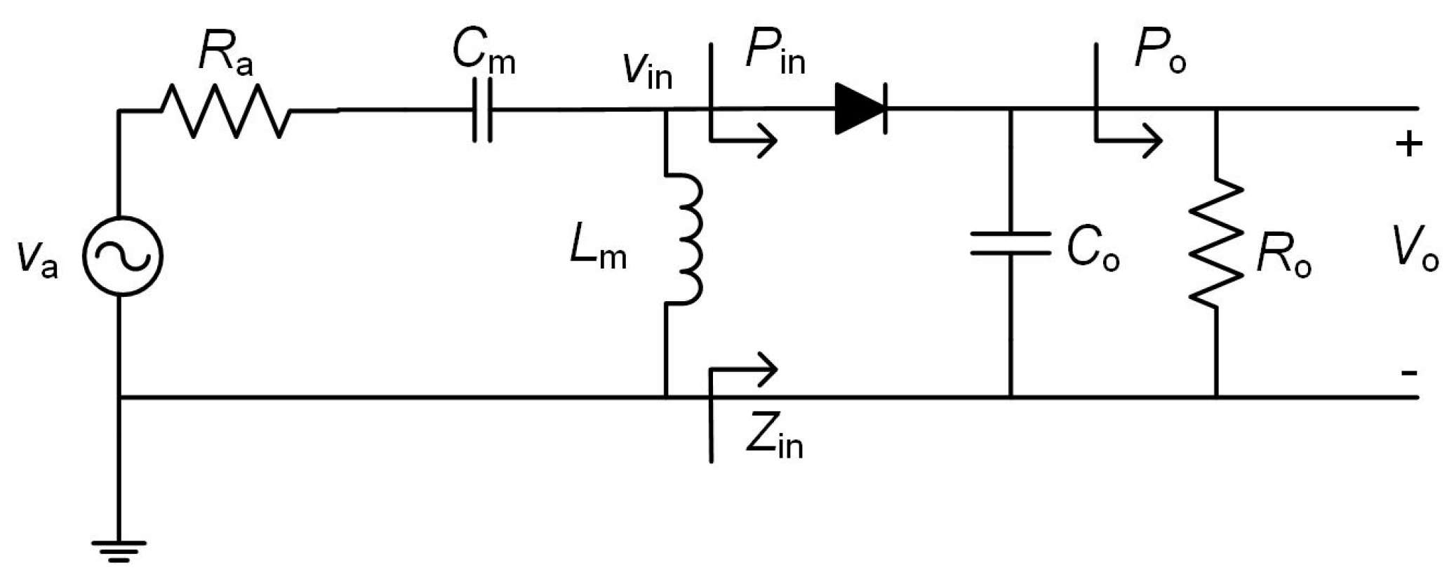
Figure 3.
Equivalent circuit of the rectenna.

Figure 4.
Equivalent circuit of the rectenna taking into account the inductor model of Figure A4 with R2 neglected.
Figure 4.
Equivalent circuit of the rectenna taking into account the inductor model of Figure A4 with R2 neglected.

Figure 5.
Qualitative graphs of the efficiencies of the rectenna versus Gt.
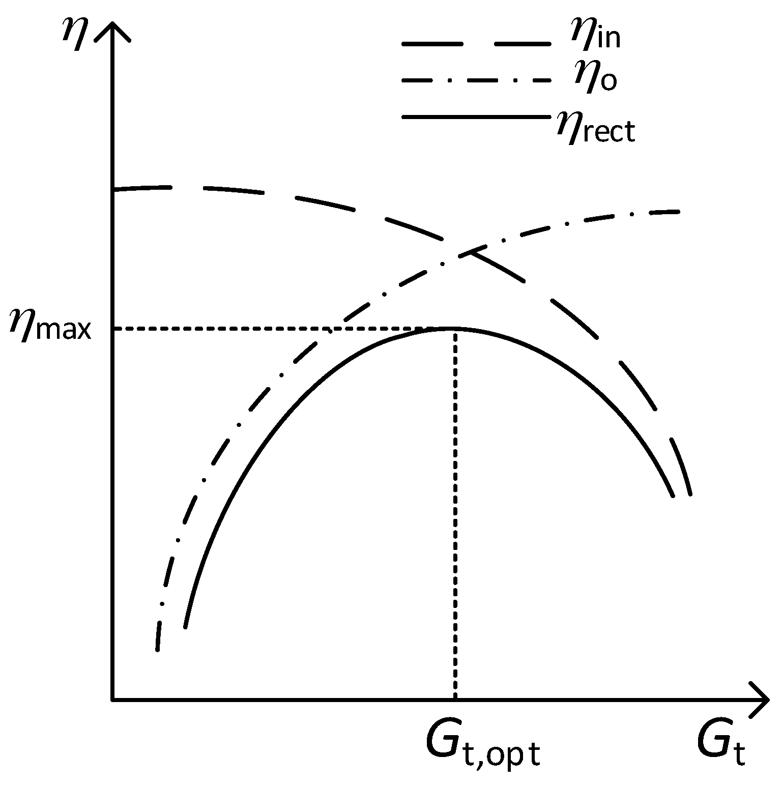
Figure 6.
PCB Layout of the rectenna with indication to the placement of the components.
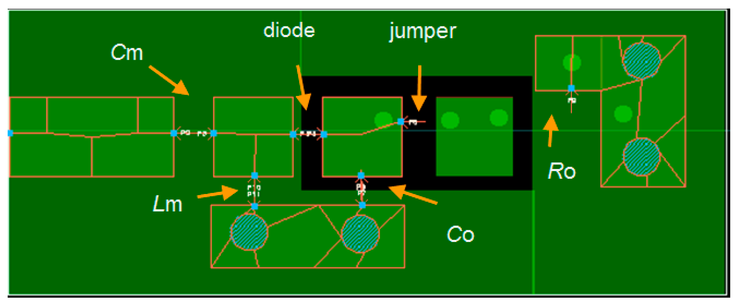
Figure 7.
Simulation results of ηrect versus Ro for several values of Lm at Cm = 0.5 pF (Gt = 3.7) and Pav = −10 dBm.
Figure 7.
Simulation results of ηrect versus Ro for several values of Lm at Cm = 0.5 pF (Gt = 3.7) and Pav = −10 dBm.

Figure 8.
Simulation results of ηrect for several values of Gt at Pav = −10 dBm. A maximum value (ηmax) of 55.2% was achieved at Gt = 3.7 (Cm = 0.5 pF).
Figure 8.
Simulation results of ηrect for several values of Gt at Pav = −10 dBm. A maximum value (ηmax) of 55.2% was achieved at Gt = 3.7 (Cm = 0.5 pF).
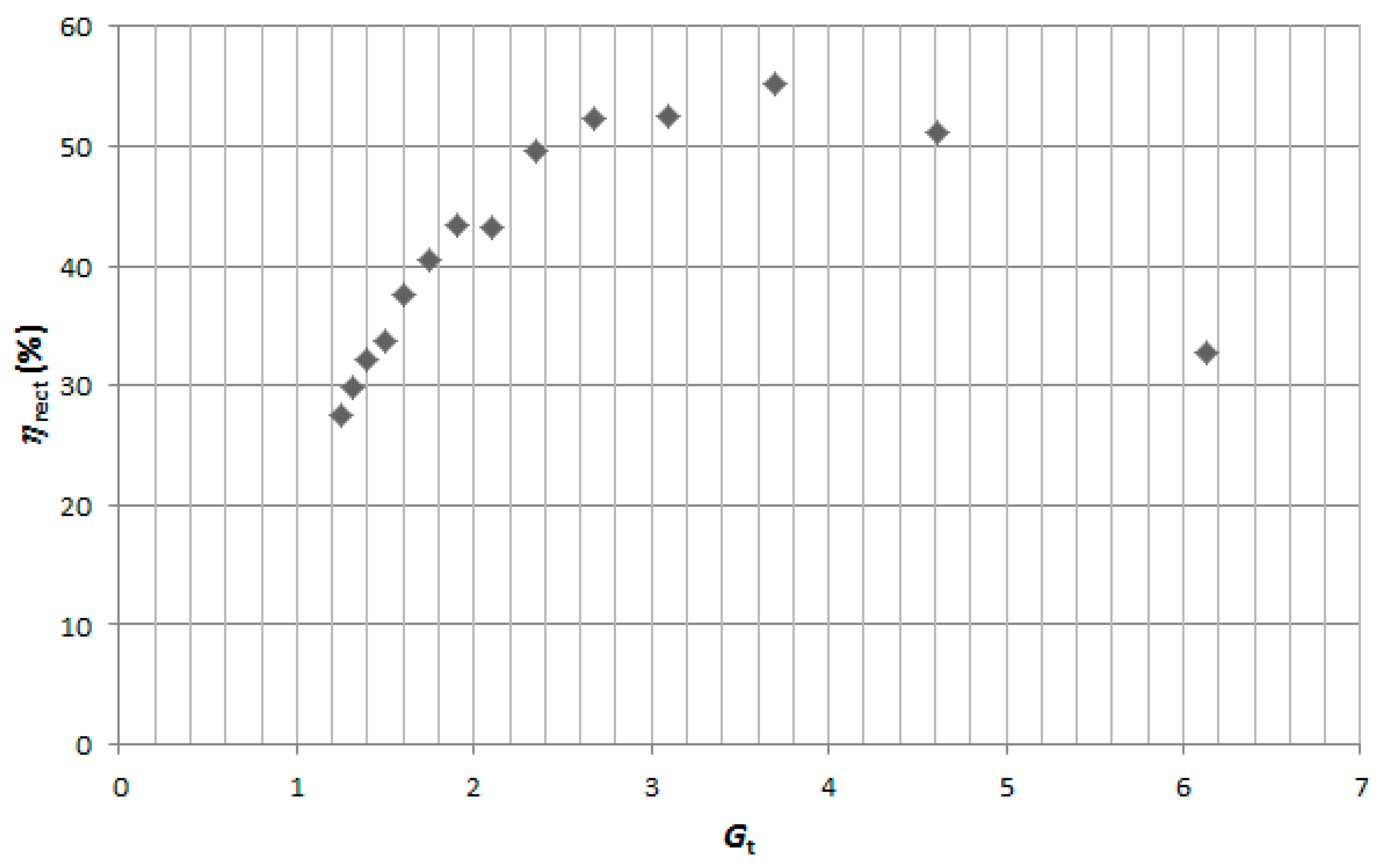
Figure 9.
Experimental results of |S11|for different power levels.


Table 1.
Values of ηmax along with the optimal values of Gt, Cm, Lm, Ro and Vo.
| Pav (dBm) | ηmax (%) | Gt | Cm (pF) | Lm (nH) | Ro (kΩ) | Vo (mV) |
|---|---|---|---|---|---|---|
| −30 | 10.9 | 5.48 | 0.3 | 30 | 8.6 | 30.7 |
| −25 | 18.6 | 5.48 | 0.3 | 30 | 7.0 | 64.2 |
| −20 | 30.8 | 3.70 | 0.5 | 27 | 4.6 | 119 |
| −15 | 44.6 | 3.70 | 0.5 | 27 | 4.4 | 249 |
| −10 | 55.2 | 3.70 | 0.5 | 27 | 4.0 | 470 |
Table 2.
Values of the input impedance of the rectenna at 814 MHz using for Ro the values of Table 1 .
Table 2.
Values of the input impedance of the rectenna at 814 MHz using for Ro the values of Table 1 .
| Pav (dBm) | −30 | −25 | −20 | −15 | −10 |
|---|---|---|---|---|---|
| Impedance (Ω) | 67.3 + j22.4 | 65.9 + j18.8 | 59.6 + j10.7 | 60.7 − j9.9 | 62.3 − j11.7 |
Table 3.
Experimental results of ηmax, Ro, and Vo.
| Pav (dBm) | ηmax (%) | Ro (kΩ) | Vo (mV) |
|---|---|---|---|
| −30 | 15.7 | 5.7 | 30 |
| −25 | 24.6 | 4.6 | 60 |
| −20 | 36.0 | 4.7 | 130 |
| −15 | 47.2 | 4.5 | 260 |
| −10 | 55.2 | 4.5 | 500 |
Table 4.
Comparative of the rectenna efficiency (%) of this work with other papers with similar designs.
© 2017 by the authors. Licensee MDPI, Basel, Switzerland. This article is an open access article distributed under the terms and conditions of the Creative Commons Attribution (CC BY) license (http://creativecommons.org/licenses/by/4.0/).
Share and Cite
MDPI and ACS Style
Gasulla, M.; Jordana, J.; Robert, F.-J.; Berenguer, J. Analysis of the Optimum Gain of a High-Pass L-Matching Network for Rectennas. Sensors 2017, 17, 1712. https://doi.org/10.3390/s17081712
AMA Style
Gasulla M, Jordana J, Robert F-J, Berenguer J. Analysis of the Optimum Gain of a High-Pass L-Matching Network for Rectennas. Sensors. 2017; 17(8):1712. https://doi.org/10.3390/s17081712
Chicago/Turabian StyleGasulla, Manel, Josep Jordana, Francesc-Josep Robert, and Jordi Berenguer. 2017. "Analysis of the Optimum Gain of a High-Pass L-Matching Network for Rectennas" Sensors 17, no. 8: 1712. https://doi.org/10.3390/s17081712
Note that from the first issue of 2016, this journal uses article numbers instead of page numbers. See further details here.