Parametric Optimization of Lateral NIPIN Phototransistors for Flexible Image Sensors


School of Electrical Engineering and Computer Science (EECS), Gwangju Institute of Science and Technology (GIST), 123, Chemdangwagi-ro, Buk-gu, 61005 Gwangju, Korea
*
Author to whom correspondence should be addressed.
†
These authors contributed equally to this work.
Sensors 2017, 17(8), 1774; https://doi.org/10.3390/s17081774
Submission received: 29 June 2017
/
Revised: 28 July 2017
/
Accepted: 29 July 2017
/
Published: 2 August 2017
(This article belongs to the Special Issue Flexible Electronics and Sensors)
Abstract
:Curved image sensors, which are a key component in bio-inspired imaging systems, have been widely studied because they can improve an imaging system in various aspects such as low optical aberrations, small-form, and simple optics configuration. Many methods and materials to realize a curvilinear imager have been proposed to address the drawbacks of conventional imaging/optical systems. However, there have been few theoretical studies in terms of electronics on the use of a lateral photodetector as a flexible image sensor. In this paper, we demonstrate the applicability of a Si-based lateral phototransistor as the pixel of a high-efficiency curved photodetector by conducting various electrical simulations with technology computer aided design (TCAD). The single phototransistor is analyzed with different device parameters: the thickness of the active cell, doping concentration, and structure geometry. This work presents a method to improve the external quantum efficiency (EQE), linear dynamic range (LDR), and mechanical stability of the phototransistor. We also evaluated the dark current in a matrix form of phototransistors to estimate the feasibility of the device as a flexible image sensor. Moreover, we fabricated and demonstrated an array of phototransistors based on our study. The theoretical study and design guidelines of a lateral phototransistor create new opportunities in flexible image sensors.
1. Introduction
Imaging systems incorporating bioinspired designs can provide many advantages compared to the conventional imaging devices [1,2,3,4,5]. Mimicking hemispherical retinas or ommatidia of animals is a core concept in bio-inspired imaging systems. A curved image sensor, which is analogous to the retina, can provide a simple configuration and a small volume of the optical system, while maintaining high optical performance [6,7]. Many researchers have reported various approaches to fabricate a curved image sensor, based on advancements of fabrication techniques and materials. Examples include a mechanically curved commercial image sensor [8,9,10,11], a photodetector array based on organic/nanomaterials [12,13,14,15,16], and the use of structured Si that is deformable in 3D [1,2,3,17]. Among them, Si-based electronics have inherent advantages such as an abundance of Si, mature technology, stability, and optical/electrical superiority. On this basis, Si-based flexible electronic devices are not limited to image sensors but are being studied for use in various flexible and wearable devices such as solar cells/photodiodes [18,19,20], tactile/pressure/temperature sensors [21,22], and health monitors [23,24].
Fundamentally, bulk Si can be easily fractured and fail due to its brittleness and rigidity. To secure the flexibility of Si, the thickness of the Si layer should be under tens of micrometers [25,26]. In addition to the use of thin Si, geometrical optimization including the electrodes has been intensely conducted for a large radius of curvature and a high density of photodetector arrays accompanying mechanical stability [27,28]. In these studies, many authors discussed the superiority and strength of the curved photodetector. Although a NIP photodiode (PD) [17,29] or a NIPINphototransistor (PTR) [1,2,3] has been widely used as a single pixel of a curved photodetector array, optimization or comparison of these single pixels has not been conducted. As the curved image sensor consists of thin Si devices, the absorption efficiency of the devices is inherently limited by the film-type active cell. Therefore, device optimization with respect to electronics is necessary for flexible and curved electronics.
Here, we present an optimized single pixel in terms of electrical aspects based on theoretical analyses. In this study, we compared a lateral NIP PD and a NIPIN PTR with the same doping concentration and thickness. From this comparison, we established that the phototransistor is a promising element as the single cell of curved photodetector arrays. To investigate the effects of other parameters with respect to semiconductor electronics, we performed a quantitative analysis of the thickness of the active cell, the doping concentration, and the structural geometry. To verify the validity on our analyses, we fabricated and measured phototransistor arrays that are designed based on our simulation. Also, we present simulations of the passive matrix characteristics of the photodetector array. Finally, we carry out a geometrical study of a single cell to enhance the cell efficiency and the mechanical stability. All simulations in our paper are based on uniform doping distribution and a carrier concentration of pure silicon (1010 cm−3) for reducing required computational memory and time.
2. Simulation and Optimization of Single Device
2.1. Comparison between Photodiode and Phototransistor
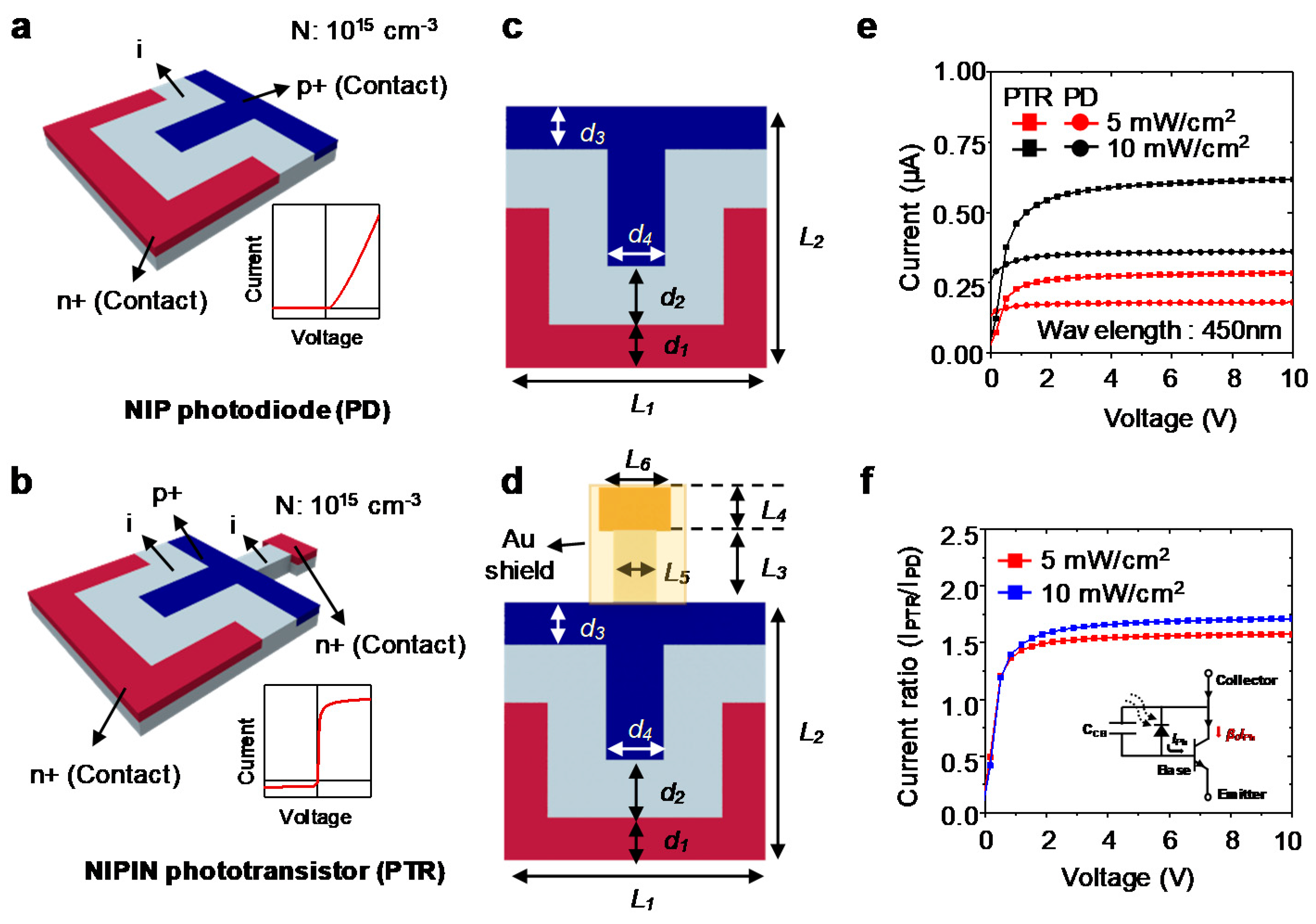
Before starting an in-depth study of the device, it is necessary to compare the NIP PD and NIPIN PTR. First, we used the same geometry of the single PTR cell reported in [2] for our study. For a thorough comparison, we set the same active region and size for the PD and PTR. From the fundamental PTR structure, the NIP PD structure was determined by removing small intrinsic and n+ doping regions, as shown in Figure 1a. Also, for the PTR, we screened a small intrinsic, and n+ doping region using a gold layer for preventing unwanted light absorption in this region [30,31]. The specific geometrical parameters for the NIP photodiode and the NIPIN phototransistor are listed in Table 1. Both devices have a doping depth of 500 nm, and the n+ and p+ regions have a doping concentration of 1015 cm−3, respectively. In the PTR and PD structures, a finger-type doping region was exploited to reduce the loss of the photo-generated carriers using the side depletion region between the n+ region and the p+ region [32]. This also broadens the active region producingphoto-generated carriers, which increases the cell efficiency. For the operation of PD, the n+ and p+ regions are contacted by an Au electrode, whereas the emitter n+ and collector n+ regions are contact areas of the Au electrode and Si in the PTR.
For a comparison of the IV characteristics between both devices, these characteristics were simulated at a light intensity of 5 mW/cm2 and 10 mW/cm2, at a wavelength of 450 nm (Figure 1e). At the same bias point, the phototransistor has a higher photocurrent. Our PTR device is a photo-bipolar junction transistor (BJT) that has a floating base. This floating base and base-collector junction are used as an absorption region for the light. For a photo-BJT in active mode, the holes generated from the absorption region accumulate in the base region. This surplus accumulated charge allows the emitter to inject electrons into the base. Since this mechanism causes an internal gain in the device, the PTR has a higher photocurrent than the PD [33]. Figure 1f shows the difference in I-V performance between the PD and the PTR due to the gain. Because of the gain, the PTR provides a possible solution to the low responsivity of a curved photodetector array owing to the thin film-type structure.
2.2. Thickness Simulation
The thickness of the active cell is a major factor in the performance of a photodetector. The characteristics of a photodetector depend strongly on the wavelength because the depth of penetration in Si varies according to the wavelength [34]. In a lateral phototransistor, carriers can be generated more efficiently at a shorter wavelength because the depletion region in the phototransistor is formed near the surface. Also, the thickness of the cell affects the flexibility of the device. For instance, a 1 μm thick Si has a bending curvature of around 104 m−1, whereas a 10 μm thick Si has a bending curvature of around 103 m−1 [25,26]. In this simulation, the doping concentration at the n+ and p+ regions was 1015 cm−3 and the thicknesses are 1.25 μm, 2.5 μm, 5 μm, and 10 μm, respectively. Figure 2a shows each EQE with different thicknesses of the phototransistor. As expected, the thicker device has a high EQE due to a long penetration depth in Si for such a long wavelength. However, increasing the thickness not only increases the EQE but also the dark current. The dark current is a noise factor in a photodetector because it is generated regardless of the input light. One of the strong sources of the dark current is thermally generated minority carriers within the bulk-Si region [35]. In addition to thermally generated carriers, for a lateral phototransistor fabricated on a bulk Si substrate, the difference in free carrier concentration between the intrinsic bulk-Si region and the depletion region creates a sharp concentration gradient. This discontinuity of the interface between the depletion and intrinsic Si bulk region causes minority carrier diffusion into the depletion region, which contributes to the dark current. For these reasons, the thicker Si PTR has a higher dark current than a thin PTR, as illustrated in Figure 2b.
An important figure of merit for an image sensor is the linear dynamic range (LDR), which determines the sensitivity of an image sensor. The LDR in the image sensor follows the equation below [36].
where Idark is the dark current and IPhoto is the measured photocurrent. Therefore, the ratio of dark current to photo-current should be considered for the use of the image sensor. Figure 2c shows the ratio of dark current to average photo-current with wavelengths of 450, 550, and 650 nm as a function of irradiance. It is seen that the 1.25 μm thick devices have a larger dynamic range than the devices with other thickness values due to the small dark current. Moreover, Figure 2d shows that the Si PTR with a thickness of 1.25 μm has a large dynamic range from the short wavelength range to a long wavelength range. From these results, although the cell should be thin for flexibility, a thin Si PTR can be applied as an image sensor owing to the large dynamic range.
Linear dynamic range = 20Log(IPhoto/Idark) dB
2.3. Doping Concentration Simulation
The doping concentration affects the device performance of a phototransistor. The doping concentration determines the width of the depletion region of the intrinsic region, which affects not only light absorption but also the recombination of minority carriers [34]. This also determines the current gain of the internal BJT [37]. Around the depletion region, the main carriers may diffuse into the relative region and can recombine with the main carriers in the other region. In this process, the generated holes and electrons disappear. In the case of high impurity concentration, the number of main carriers increases, enabling recombination with other carriers in a short distance. In other words, the depletion layer becomes thinner. Otherwise, in a semiconductor junction with a low impurity concentration, the depletion layer is thick because the recombination requires a further distance.
To investigate the effects of doping concentration, several simulations were performed on a device that equally doped p+ and n+ regions with a thickness of 1.25 μm. Figure 3b shows the conduction band at zero bias for a cross section of Figure 3a. The incident light generates electron-hole pairs at the base region, which lowers the conduction band of the base region. This result shows the band profiles of the device become different depending on doping concentrations and light intensities at a wavelength of 450 nm. In the case of low doping concentration (i.e., 1013 cm−3), the conduction band becomes lower as the incident light becomes stronger. Eventually, the conduction band is flattened at irradiance of 10−2 W/cm2. Contrastively, the device with high doping concentration maintains a conduction band relatively well as the incident light becomes stronger. In the conduction band, the devices with higher doping concentrations keeps the band shape well under strong light illuminations.
Based on the theoretical analyses with the conduction band, the tendency of PTR was investigated with respect of light intensity and doping concentration. Figure 3c shows the recombination rate for the cross sections of PTR with different doping concentrations. Heavy doping concentration causes a high recombination rate in the intrinsic region owing to the short effective carrier lifetime [38]. Figure 3d shows the integration of the recombination rate along the X direction for each doping concentration. The device with a doping concentration of 1017 cm−3 demonstrates a higher recombination rate than the other devices; however, it maintains the band shape under strong illumination. The lightly-doped devices no longer show linearity with light intensity over 10−3 W/cm2 because the characteristics of the BJT are lost (Figure 3e). The dynamic range of the device with the heavy doping concentration maintains linearity. The inset in Figure 3e exhibits the I-V characteristics for each doping concentration. Although the I-V characteristic is slightly degraded compared to that with the doping concentration of 1015 cm−3, this subtle degradation in the I-V curve is not imperative to operate as a single cell of PTR array. To investigate a practical case, the I-V curves reflecting the carrier concentration of 1014 cm−3 in the intrinsic region are simulated for the fabrication of PTR (Figure 3f). Considering both linearity and gain for an image sensor, the doping concentration of PTR should be heavier than 1015 cm−3.
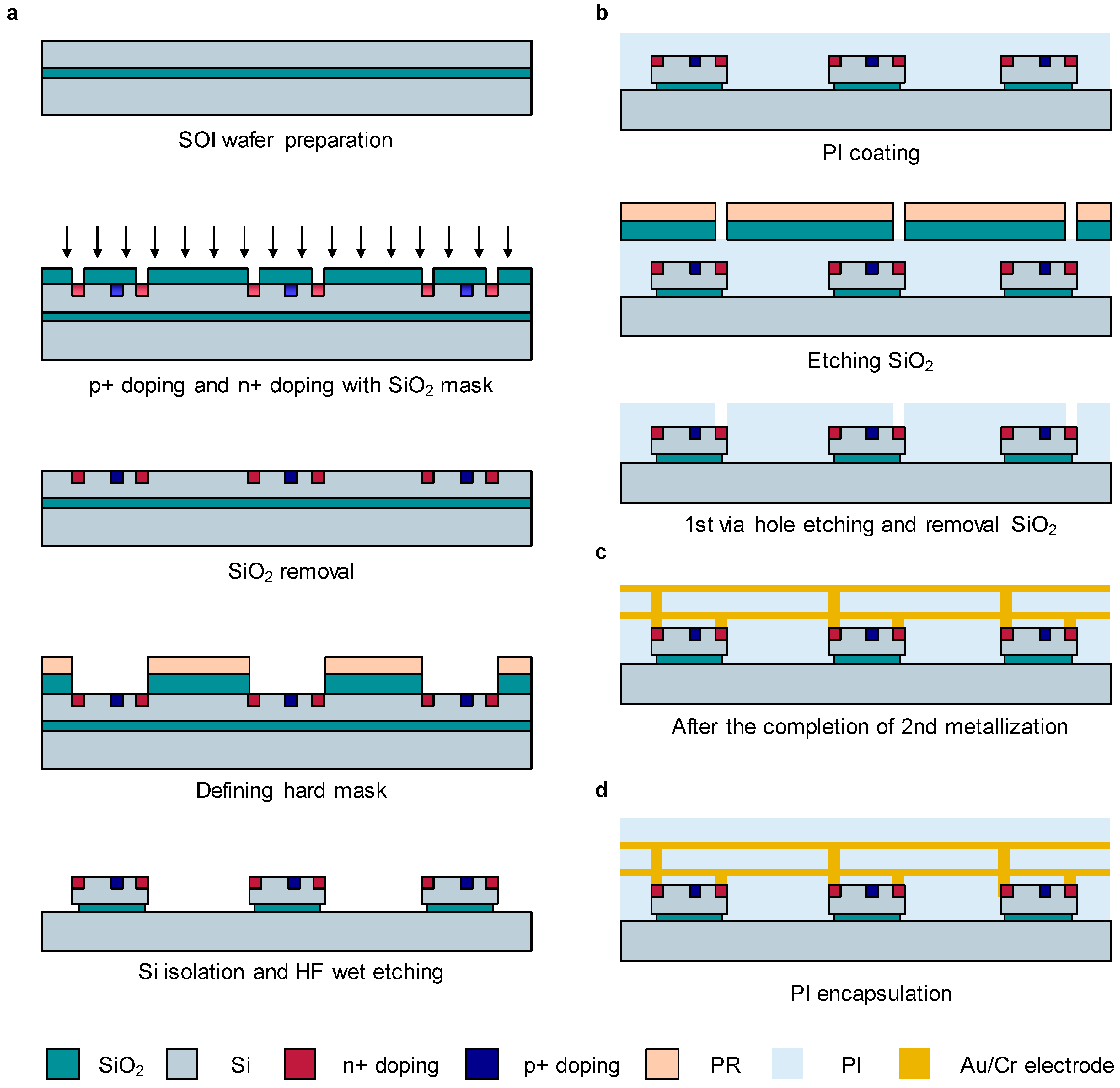
3. Fabrication of Phototransistor and Passive Matrix
The fabrication process of a curved phototransistor array is largely classified into two parts: the manufacture of the PTR and the development of a passive matrix. Figure 4 shows a schematic illustration of the fabrication process for the phototransistor and the wiring of the PTR. We used a silicon on insulator (SOI) wafer with a Si thickness of 1.25 μm, which presented the highest dynamic range, as seen in Figure 2. The thickness of the buried oxide layer is 400 nm. The following steps describe the detailed fabrication process of the phototransistor array.
Step 1: phototransistor pixel defining, as shown in Figure 4a. A SOI wafer is prepared with a cleaning process with acetone, isopropyl alcohol (IPA), and deionized (DI) water. For a doping concentration of 1015 cm−3, first, a SOI (100) wafer with a patterned SiO2 layer is exposed by diffusive boron (PDS BN 1050) at a temperature of 1000 °C for 10 min. Subsequently, phosphorous (PDS PH 1000 N) is diffused on the wafer at a temperature of 1000 °C for 10 min. After n+ and p+ doping, the annealing process is performed to restore crystallinity of Si layer with a temperature of 1000 °C for 20 min. As a hard mask for dry etching, silicon dioxide (SiO2) with a thickness of 600 nm is deposited by plasma-enhanced chemical vapor deposition (PECVD). A photoresist (PR; AZ5214, MicroChemicals, Ulm, Germany) is then spin-coated onto the sample with a speed of 3000 rpm for 30 s. Next, photolithographic patterning of the PR is followed by thermally curing the PR (60 s at 90 °C) to define the area of the phototransistor. Additional thermal curing on the sample is conducted to improve the adhesion between the PR and SiO2 (2 min at 110 °C). Afterward, the hard mask layer, SiO2, is patterned by wet etching with a buffered oxide etchant (BOE) for ~15 s. Next, naked Si is etched by an inductively coupled plasma-reactive ion etcher (ICP-RIE; 4 mTorr, 50 sccm SF6, RF 50 W, ICP 100 W, 6 min) to define the area of the device. Finally, the isolated sample is immersed in hydrogen fluoride (HF) solution for ~2 min 30 s to partly etch the edge of SiO2 under the Si layer.
Step 2: Polyimide (PI; 431176, Sigma-Aldrich, St. Louis, MO, USA) opening for wiring, as shown in Figure 4b. First, liquid-state PI is spin-coated onto the sample at 4000 rpm for 40 s to form a ~1.2 μm-thick PI layer and then cured at 230 °C for 2 h in an oven under a N2 atmosphere. A SiO2 layer with a thickness of 300 nm is deposited by PECVD at a relatively low temperature, 230 °C, to avoid thermal damage on PI. Reacting ion etching (RIE; 30 mTorr, 30 sccm O2, RF 30 W, 25 min) through a photolithographically patterned hard mask SiO2 removed the PI in the open regions. The residual PR and SiO2 layers are then removed by acetone and BOE, respectively.
Step 3: Au/Cr electrode wiring for the passive matrix of phototransistors, as shown in Figure 4c. Before the first metallization, a cleaning process is performed. Cr (~10 nm) is deposited by sputtering followed by Au deposition (~200 nm). The liquid-state PI is spin-coated and thermally cured in the oven. Next, for the second metallization, the same process outlined in Step 2 is performed to open the area for the contact of the electrode.
Step 4: PI encapsulation, as shown in Figure 4d. For protection of the devices, a third PI layer is formed by spin-coating and a thermal curing process.
4. Characterization of PTR Arrays with Passive Matrix Addressing
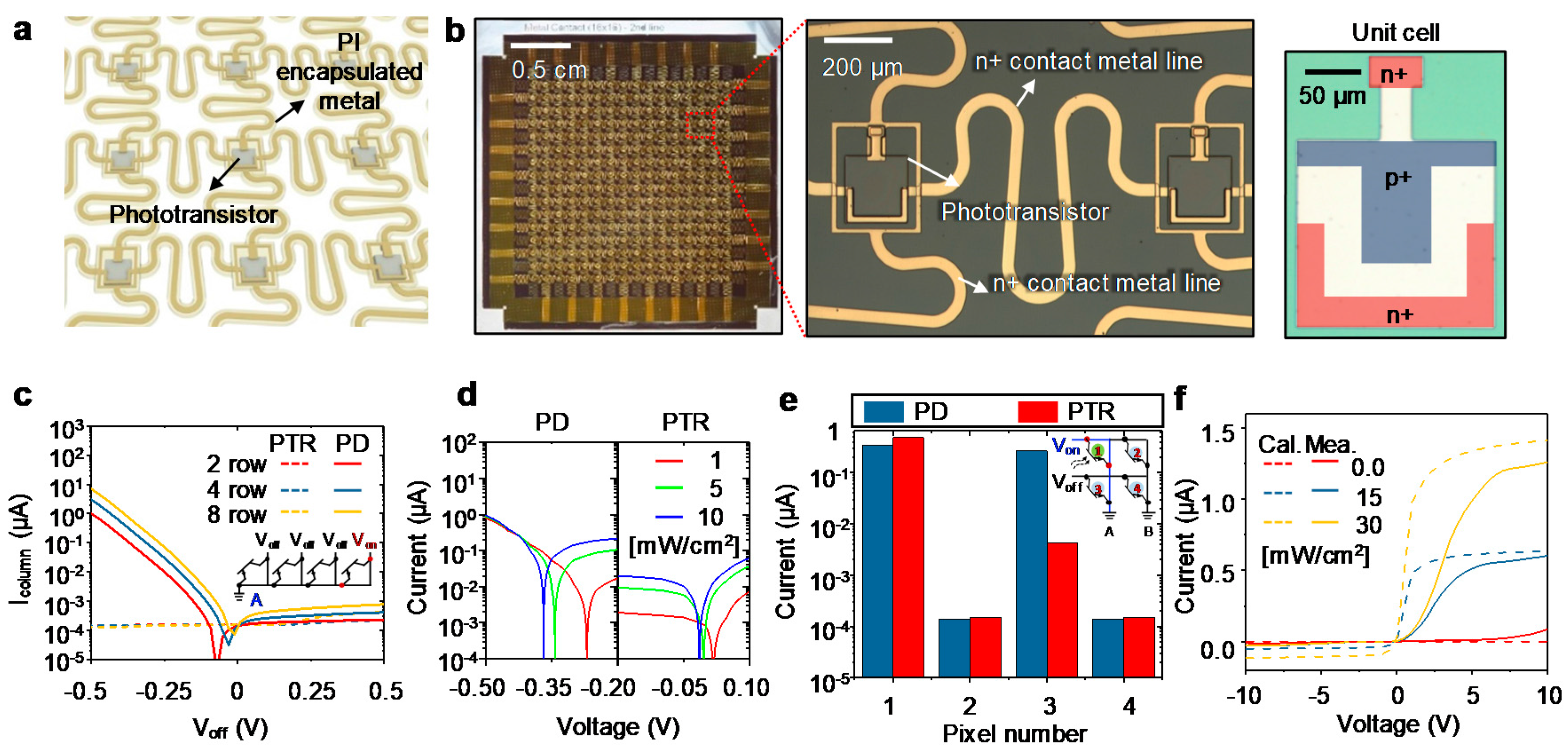
To evaluate the capability of the proposed PTR array, the characteristics of the I-V curve and crosstalk in the array form should be discussed. To this end, we fabricated a PTR array as a passive matrix type. Figure 5a illustrates the scheme of the complete PTR array. Figure 5b shows the completed PTR array consisting of 16 by 16 phototransistors (i.e., the number of pixels is 256), and magnified views after the second metallization. The unit cell in Figure 5b is the status finished up to the HF wet etching step. When a readout circuit senses the photocurrent of a given pixel, a positive voltage is applied to a row electrode on a column electrode. This bias voltage works as a reverse bias to the pixel located at the intersection of the two electrodes and causes current dominated by the photocurrent or dark current of the diode. For this reason, other pixels in the same column contribute to the dark current or photocurrent of the column current. This crosstalk in the passive matrix is defined as follows [39].
where Icolumn is the current generated from the column displayed as the inset of Figure 5c, IL is the photocurrent of the illuminated phototransistor, ID is the dark current of the non-illuminated phototransistor, and N is the number of rows. To select the pixel in the passive matrix, the bias voltage is applied to the addressed pixel against the ground, whereas zero voltage is applied to the non-addressed pixel instead of the bias voltage. However, setting zero voltage to the non-addressed pixel is difficult in a real passive matrix device. In real devices, a small voltage (close to zero) is applied to the non-addressed pixels. To investigate the current of the column, we set the voltages applied to the addressed phototransistor and non-addressed phototransistor as Von and Voff, respectively. As the current from the non-addressed phototransistor is dependent on Voff, the current influenced by Voff is an important factor in array characteristics.
Icolumn = IL,D(on) + (N − 1)IL,D(off)
Figure 5c demonstrates the feature of Icolumn with different numbers of rows (i.e., different N in Equation (2)) for NIP PD and NIPIN PTR in array forms under the dark state. In the case of the NIP PD, the variation of Voff varied significantly as N increases. Since the illumination light is absent, Icolumn is composed of dark current from other pixels, indicating the passive matrix of the PD can suffer from serious noise. Moreover, Vmin, indicating the voltage corrsponding to the minimum point of current, is affected by N, whereas the Icolumn of PTR array is unchanged upon voltage variation from −0.5 to 0.5 V. In addition to the unchanged Vmin point, the NIPIN PTR array is robust to the noise signal from adjacent pixels compared to the NIP PD array.
To reduce crosstalk in a passive matrix, a single pixel should not have variation in the Vmin caused by the external light, because the current of the active pixel sensed by the readout circuit could not be stable. Figure 5d shows the effect of the light intensity on the Vmin of a single PD and the PTR. In the case of the PTR, when the intensity of light changes from 1 mW/cm2 to 10 mW/cm2, Vmin varies by about −0.02 V. On the other hand, in the case of the PD, the difference of Vmin is −0.26 V. For insight into the meaning of Vmin, we compared the current variation at 0 V, 0.2 μA in the PD, and 5 nA in PTR. Therefore, the passive matrix, which consists of PDs, presents substantial noise from the non-addressed pixels in the presence of light owing to the fluctuation of Vmin.
Figure 5e shows the current values of PTR and PD in a two by two passive matrix form. To detect the current in the passive matrix, Von and Voff are applied to the addressed rows and non-addressed rows as 3 V and 0 V, respectively. The current values of each pixel are then read. The first pixels of PTR and PD in column A are illuminated with 10 mW/cm2, as illustrated in the inset of Figure 5e. Other pixels in columns A and B are not illuminated. However, the current value of the third pixel, which is in column A, is higher than the dark current of the second or fourth pixel, which is in column B, because it was the crosstalk of adjacent pixels in the same column. Comparing the third pixels of PD and PTR, the results demonstrate that the PD has a higher dark current than the PTR. From the results in Figure 5c–e, the passive matrix composing the PTR presents many strengths with respect to crosstalk compared to the passive matrix of the PD.
Figure 5f demonstrates the I-V curve of the fabricated PTR array with different illumination intensities: 0, 15, 30 mW/cm2. A xenon lamp with a color temperature of 5800 K (commercial light source SLS401,Thor lab) was utilized as a light source in the measurements. The slope of the curve and the saturated current are different from the calculation results because of differences in the doping profiles (i.e., uniform and Gaussian distributions) and the ideality factor changed by the light intensity [34]. The deviation from the ideality factor and doping profile is acceptable as compared to the ideal case. Also, the tendency of I-V characteristics is akin to each other. Because of this, the simulation results guide the design of PTR for fabrication.
In addition to the electrical performance of the device, the deformability of flexible and/or curved image sensors in array type should be considered. Many other methods for developing the curvilinear shape image sensors based on inorganic materials have been reported (Table 2). Traditionally, a method of bending using a pressure after thinning the thickness of a commercial image sensor has been studied [8,11]. This approach has a strength that the high-resolution imager can be utilized; however, the deformability is seriously restricted by strain. Using inorganic nanomembranes which have flexibility caused by a film-type device is one of the other methods to improve the deformability [40,41,42,43]. However, the 3-dimensional deformation of devices requires stretchability as well. On this basis, the general nanomaterial-based curved/flexible image sensor is difficult to deform into a hemispheric shape. Kirigami- and array-based image sensors can provide high deformability such as a hemispherical shape [1,2,3,17]. However, the kirigami-based image sensor is exactly fabricated to fit with a dome, limiting the curvature variation. Our approach, which is based on array type, shows the highest deformability and radius of curvature. Also, stretchable metal interconnectors between each pixel offer curvature-tunable photodetector [3].
5. Geometry Optimization
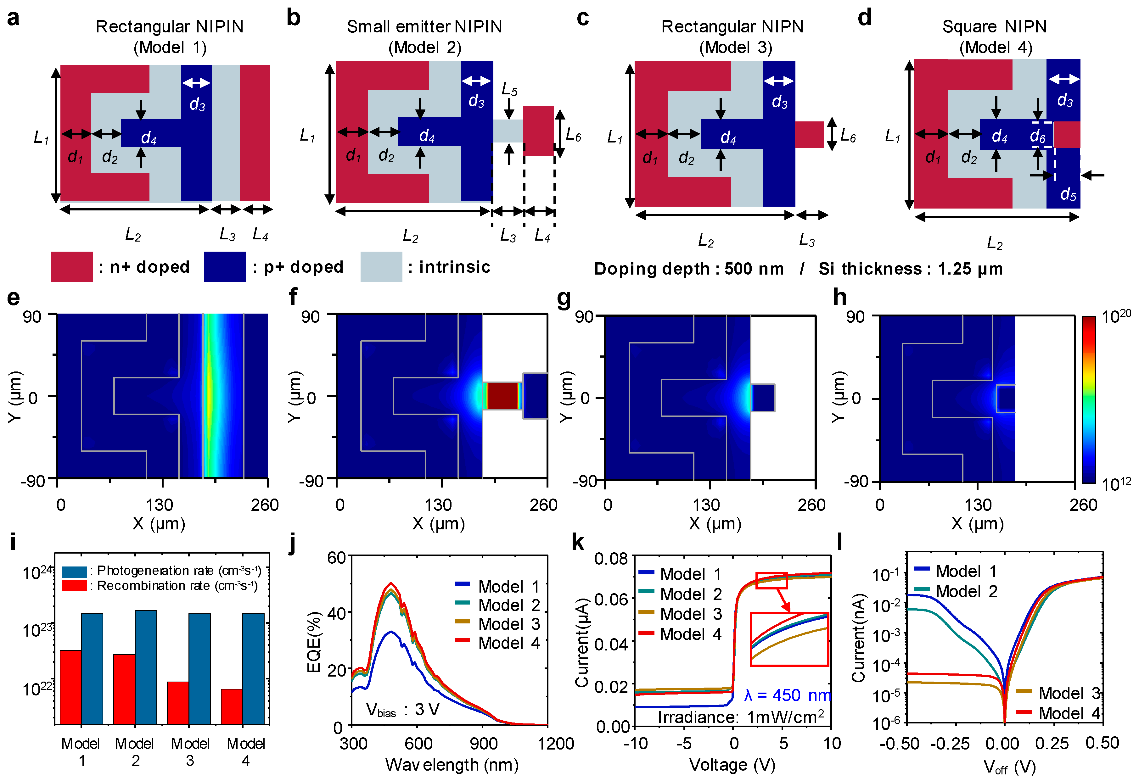
Thus far, we have discussed the advantages and excellence of the PTR as a single cell and even an array type. However, small intrinsic and n+ doping regions in this structure are exposed to the risk of fracture due to a mechanically unstable geometry. Moreover, the small intrinsic region in the PTR is not necessary in principle. Therefore, we designed and simulated four different geometries, including the fundamental structure we have discussed, to find the optimum geometry of the PTR in electrical/mechanical aspects. The detailed geometrical parameters are listed in Table 3. The first design, model 1, is a rectangular NIPIN model, where the intrinsic and n+ doping regions are expanded from the design we have studied (Figure 6a). Model 2 is our basic design, which is effective to reduce the recombination rate from the intrinsic region (Figure 6b). To suppress the recombination rate further, the intrinsic region is removed followed by direct contact with the n+ doping region to the p+ doping region (Figure 6c). In model 4, a n+ doping region is inserted into the p+ doping region, which is the most stable geometry mechanically (Figure 6d).
Figure 6e–h displays the recombination rate in the plane 50 nm from the surface for each model. In models 1 and 2, strong recombination occurs in the intrinsic regions, whereas models 3 and 4, which do not have the intrinsic region, show comparatively weak recombination. Figure 6i presents the total recombination by summation of all recombination rates in the contour plots, and it also gives the total photogeneration rate in the same planes. These results demonstrate the low recombination rates in the designs without intrinsic regions, while similar photogeneration rates are obtained. Model 4 has the highest EQE among all models, as illustrated in Figure 6j. This can be explained by the low recombination rate. Simulations of I-V curves for each model are also conducted, as shown in Figure 6k. In the active range, all devices represent comparable current versus voltage features, but model 1 has a vast amount of current in the range of negative voltage due to the wide intrinsic region. In the array form, the feature of Voff is imperative because it is equivalent to the noise signal to the active cell. From this point of view, the devices without the intrinsic region are appropriate as the pixels of a photodetector array, as demonstrated in Figure 6l. With consideration of mechanical and electrical aspects, model 4 is the most promising cell geometry for the curved photodetector array.
6. Conclusions
In this paper, we investigated a lateral NIPIN phototransistor (PTR) array, which was reported in previous research [2], under different conditions such as thickness and doping concentration. We first compared the NIPIN PTR and PIN photodiode (PD) as a pixel of the curved photodetector array. This comparison showed that the NIPIN PTR can be a solution to address low absorption efficiency of the active cell owing to the film-type device. Also, because the thin active cell has an advantage with respect to the dark current, a large dynamic range can be realized compared to that of a thick Si PTR. Also, we have designed and simulated the optimum geometry of the PTR for a curved photodetector array in both mechanical and electrical aspects. The optimized structure (Model 4) in this paper will be experimentally fabricated and demonstrated as future work. We also fabricated the PTR array to examine the validity of our simulations. In the fabrication process, a silicon on insulator (SOI) wafer with an Si thickness of 1.25 μm was doped by a molecular diffusion process of phosphorous and boron at 1000 °C for 10 min. Subsequently, the annealing treatment was performed at 1000 °C for 20 min. The PTR was fabricated through a series of semiconductor fabrication processes including deposition, photolithographical patterning, and etching.
Thus far, in the field of flexible/wearable electronics, although there has been intensive research on the mechanical/material components of devices, theoretical studies on optimization regarding electronics have not yet been conducted. In this light, the proposed PTR can provide a design rule for high-efficiency Si-based flexible/wearable optoelectronic devices.
Acknowledgments
This work was supported by the National Research Foundation of Korea (NRF) grant funded by the South Korean government (NRF-2017R1D1A1B03028055). This work was also supported by the DGIST R&D Program of Ministry of Science and ICT of Korea (Grant No. 17-DB-02).
Author Contributions
M.S.K. and G.J.L. contributed equally to this work. M.S.K. and H.M.K. performed TCAD simulation and analyzed simulation data. G.J.L. and H.M.K. focused on the measurement setup, device fabrication, and experiment. The manuscript was written through the contribution of G.J.L. and M.S.K. Y.M.S. provided suggestions about the work and helped to modify the manuscript. All authors read and approved the final manuscript.
Conflicts of Interest
The authors declare no conflict of interest.
References
- Ko, H.C.; Stoykovich, M.P.; Song, J.; Malyarchuk, V.; Choi, W.M.; Yu, C.-J.; Geddes, J.B., III; Xiao, J.; Wang, S.; Huang, Y.; et al. A hemispherical electronic eye camera based on compressible silicon optoelectronics. Nature 2008, 454, 748–753. [Google Scholar] [CrossRef] [PubMed]
- Song, Y.M.; Xie, Y.; Malyarchuk, V.; Xiao, J.; Jung, I.; Choi, K.-J.; Liu, Z.; Park, H.; Lu, C.; Kim, R.-H.; et al. Digital cameras with designs inspired by the arthropod eye. Nature 2013, 497, 95–99. [Google Scholar] [CrossRef] [PubMed]
- Jung, I.; Xiao, J.; Malyarchuk, V.; Lu, C.; Li, M.; Liu, Z.; Yoon, J.; Huang, Y.; Rogers, J.A. Dynamically tunable hemispherical electronic eye camera system with adjustable zoom capability. Proc. Natl. Acad. Sci. USA 2011, 108, 1788–1793. [Google Scholar] [CrossRef] [PubMed]
- Floreano, D.; Pericet-Camara, R.; Viollet, S.; Ruffier, F.; Brückner, A.; Leitel, R.; Buss, W.; Menouni, M.; Expert, F.; Juston, R.; et al. Miniature curved artificial compound eyes. Proc. Natl. Acad. Sci. USA 2013, 110, 9267–9272. [Google Scholar] [CrossRef] [PubMed] [Green Version]
- Liu, H.; Huang, Y.; Jiang, H. Artificial eye for scotopic vision with bioinspired all-optical photosensitivity enhancer. Proc. Natl. Acad. Sci. USA 2016, 113, 3982–3985. [Google Scholar] [CrossRef] [PubMed]
- Pang, K.; Fang, F.; Song, L.; Zhang, Y.; Zhang, H. Bionic compound eye for 3D motion detection using an optical freeform surface. J. Opt. Soc. Am. B 2017, 34, B28–B35. [Google Scholar] [CrossRef]
- Lee, G.J.; Nam, W.I.L.; Song, Y.M. Robustness of an artificially tailored fisheye imaging system with a curvilinear image surface. Opt. Laser Technol. 2017, 96, 50–57. [Google Scholar] [CrossRef]
- Dumas, D.; Fendler, M.; Berger, F.; Cloix, B.; Pornin, C.; Baier, N.; Druart, G.; Primot, J.; Le Coarer, E. Infrared camera based on a curved retina. Opt. Lett. 2012, 37, 653–655. [Google Scholar] [CrossRef] [PubMed]
- Dumas, D.; Fendler, M.; Baier, N.; Primot, J.; le Coarer, E. Curved focal plane detector array for wide field cameras. Appl. Opt. 2012, 51, 5419–5424. [Google Scholar] [CrossRef] [PubMed]
- Gregory, J.A.; Smith, A.M.; Pearce, E.C.; Lambour, R.L.; Shah, R.Y.; Clark, H.R.; Warner, K.; Osgood, R.M.; Woods, D.F.; DeCew, A.E. Development and application of spherically curved charge-coupled device imagers. Appl. Opt. 2015, 54, 3072–3082. [Google Scholar] [CrossRef] [PubMed]
- Guenter, B.; Joshi, N.; Stoakley, R.; Keefe, A.; Geary, K.; Freeman, R.; Hundley, J.; Patterson, P.; Hammon, D.; Herrera, G. Highly curved image sensors: A practical approach for improved optical performance. Opt. Express 2017, 25, 13010–13023. [Google Scholar] [CrossRef]
- Xu, X.; Mihnev, M.; Taylor, A.; Forrest, S.R. Organic photodetector arrays with indium tin oxide electrodes patterned using directly transferred metal masks. Appl. Phys. Lett. 2009, 94, 1–3. [Google Scholar] [CrossRef]
- Deng, W.; Zhang, X.; Huang, L.; Xu, X.; Wang, L.; Wang, J.; Shang, Q.; Lee, S.; Jie, J. Aligned Single-Crystalline Perovskite Microwire Arrays for High-Performance Flexible Image Sensors with Long-Term Stability. Adv. Mater. 2016, 28, 2201–2208. [Google Scholar] [CrossRef] [PubMed]
- Liu, X.; Lee, E.K.; Kim, D.Y.; Yu, H.; Oh, J.H. Flexible organic phototransistor array with enhanced responsivity via metal–ligand charge transfer. ACS Appl. Mater. Interfaces 2016, 8, 7291–7299. [Google Scholar] [CrossRef] [PubMed]
- Li, X.; Yu, D.; Chen, J.; Wang, Y.; Cao, F.; Wei, Y.; Wu, Y.; Wang, L.; Zhu, Y.; Sun, Z. Constructing fast carrier tracks into flexible perovskite photodetectors to greatly improve responsivity. ACS Nano 2017, 11, 2015–2023. [Google Scholar] [CrossRef] [PubMed]
- Li, L.; Gu, L.; Lou, Z.; Fan, Z.; Shen, G. ZnO Quantum Dot Decorated Zn2SnO4 Nanowire Heterojunction Photodetectors with Drastic Performance Enhancement and Flexible Ultraviolet Image Sensors. ACS Nano 2017, 11, 4067–4076. [Google Scholar] [CrossRef] [PubMed]
- Wu, T.; Hamann, S.S.; Ceballos, A.C.; Chang, C.E.; Solgaard, O.; Howe, R.T. Design and fabrication of silicon-tessellated structures for monocentric imagers. Microsyst. Nanoeng. 2016, 2, 16019. [Google Scholar] [CrossRef]
- Yoon, J.; Li, L.; Semichaevsky, A.V.; Ryu, J.H.; Johnson, H.T.; Nuzzo, R.G.; Rogers, J.A. Flexible concentrator photovoltaics based on microscale silicon solar cells embedded in luminescent waveguides. Nat. Commun. 2011, 2, 343. [Google Scholar] [CrossRef] [PubMed]
- Lee, S.-M.; Biswas, R.; Li, W.; Kang, D.; Chan, L.; Yoon, J. Printable nanostructured silicon solar cells for high-performance, large-area flexible photovoltaics. ACS Nano 2014, 8, 10507–10516. [Google Scholar] [CrossRef] [PubMed]
- Kang, D.; Gai, B.; Thompson, B.; Lee, S.-M.; Malmstadt, N.; Yoon, J. Flexible Opto-Fluidic Fluorescence Sensors Based on Heterogeneously Integrated Micro-VCSELs and Silicon Photodiodes. ACS Photonics 2016, 3, 912–918. [Google Scholar] [CrossRef]
- Kim, J.; Lee, M.; Shim, H.J.; Ghaffari, R.; Cho, H.R.; Son, D.; Jung, Y.H.; Soh, M.; Choi, C.; Jung, S. Stretchable silicon nanoribbon electronics for skin prosthesis. Nat. Commun. 2014, 5, 5747. [Google Scholar] [CrossRef] [PubMed]
- Song, J.-K.; Son, D.; Kim, J.; Yoo, Y.J.; Lee, G.J.; Wang, L.; Choi, M.K.; Yang, J.; Lee, M.; Do, K.; et al. Wearable force touch sensor array using a flexible and transparent electrode. Adv. Funct. Mater. 2016, 27, 1–9. [Google Scholar] [CrossRef]
- Van den Brand, J.; de Kok, M.; Koetse, M.; Cauwe, M.; Verplancke, R.; Bossuyt, F.; Jablonski, M.; Vanfleteren, J. Flexible and stretchable electronics for wearable health devices. Solid State Electron. 2015, 113, 116–120. [Google Scholar] [CrossRef]
- Yu, K.J.; Kuzum, D.; Hwang, S.-W.; Kim, B.H.; Juul, H.; Kim, N.H.; Won, S.M.; Chiang, K.; Trumpis, M.; Richardson, A.G. Bioresorbable silicon electronics for transient spatiotemporal mapping of electrical activity from the cerebral cortex. Nat. Mater. 2016, 15, 782–791. [Google Scholar] [CrossRef] [PubMed]
- Lu, N. Mechanics, materials, and functionalities of biointegrated electronics. Bridge 2013, 43, 31–38. [Google Scholar]
- Burghartz, J.N.; Appel, W.; Harendt, C.; Rempp, H.; Richter, H.; Zimmermann, M. Ultra-thin chip technology and applications, a new paradigm in silicon technology. Solid State Electron 2010, 54, 818–829. [Google Scholar] [CrossRef]
- Shin, G.; Jung, I.; Malyarchuk, V.; Song, J.; Wang, S.; Ko, H.C.; Huang, Y.; Ha, J.S.; Rogers, J.A. Micromechanics and advanced designs for curved photodetector arrays in hemispherical electronic-eye cameras. Small 2010, 6, 851–856. [Google Scholar] [CrossRef] [PubMed]
- Jung, I.; Shin, G.; Malyarchuk, V.; Ha, J.S.; Rogers, J.A. Paraboloid electronic eye cameras using deformable arrays of photodetectors in hexagonal mesh layouts. Appl. Phys. Lett. 2010, 96, 021110. [Google Scholar] [CrossRef]
- Dang, M.; Yuan, H.-C.; Ma, Z.; Ma, J.; Qin, G. The fabrication and characterization of flexible single-crystalline silicon and germanium p-intrinsic-n photodetectors on plastic substrates. Appl. Phys. Lett. 2017, 110, 253104. [Google Scholar] [CrossRef]
- Chang, J.H.; Vygranenko, Y.; Nathan, A. Two-dimensional a-Si: H based nip sensor array. J. Vac. Sci. Technol. A 2004, 22, 971–974. [Google Scholar] [CrossRef]
- De Cesare, G.; Di Rosa, P.; La Monica, S.; Salotti, R.; Rita, R.; Schirone, L. Addressable Photosensing Elements for 2-Dimensional Image Sensors Using a-Si Alloy PIN Diodes. Mat. Res. Soc. Symp. Proc. 1993, 297. [Google Scholar] [CrossRef]
- Shin, K.-S.; Kim, Y.-H.; Paek, K.-K.; Park, J.-H.; Yang, E.-G.; Kim, T.-S.; Kang, J.-Y.; Ju, B.-K. Characterization of an integrated fluorescence-detection hybrid device with photodiode and organic light-emitting diode. IEEE Electron Device Lett. 2006, 27, 746–748. [Google Scholar] [CrossRef]
- Shive, J. The properties of germanium phototransistors. J. Opt. Soc. Am. 1953, 43, 239–244. [Google Scholar] [CrossRef]
- Sze, S.M. Physics of Semiconductor Devices, 3rd ed.; Wiley: New York, NY, USA, 2006. [Google Scholar]
- Deen, M.J.; Basu, P.K. Silicon Photonics: Fundamentals and Devices; Wiley: New York, NY, USA, 2012. [Google Scholar]
- Gong, X.; Tong, M.; Xia, Y.; Cai, W.; Moon, J.S.; Cao, Y.; Yu, G.; Shieh, C.-L.; Nilsson, B.; Heeger, A.J. High-Detectivity Polymer Photodetectors with Spectral Response from 300 nm to 1450 nm. Science 2009, 325, 1665–1667. [Google Scholar] [CrossRef] [PubMed]
- Shockley, W.; Sparks, M.; Teal, G.K. p−n Junction Transistors. Phys. Rev. 1951, 83, 151–162. [Google Scholar] [CrossRef]
- Schlangenotto, H.; Scheuermann, U.; De Doncker, R. Pin-Diodes. In Semiconductor Power Devices: Physics, Characteristics, Reliability; Springer: Heidelberg/Berlin, Germany, 2010; pp. 159–224. [Google Scholar]
- Braun, D.; Yu, G. Simulations of Passive Matrix Polymer Image Sensors. MRS Proc. 1999, 558. [Google Scholar] [CrossRef]
- Seo, J.-H.; Zhang, K.; Kim, M.; Zhao, D.; Yang, H.; Zhou, W.; Ma, Z. Flexible phototransistors based on single-crystalline silicon nanomembrane. Adv. Opt. Mater. 2015, 4, 120–125. [Google Scholar] [CrossRef]
- Kim, M.; Seo, J.-H.; Yu, Z.; Zhou, W.; Ma, Z. Flexible germanium nanomembrane metal-semiconductor-metal photodiodes. Appl. Phys. Lett. 2016, 109, 051105. [Google Scholar] [CrossRef]
- Fan, D.; Lee, K.; Forrest, S.R. Flexible thin-film InGaAs photodiode focal plane array. ACS Photonics 2016, 3, 670–676. [Google Scholar] [CrossRef]
- Seo, J.-H.; Ling, T.; Gong, S.; Zhou, W.; Ma, A.L.; Guo, L.J.; Ma, Z. Fast flexible transistors with a nanotrench structure. Sci. Rep. 2016, 6, 24771. [Google Scholar] [CrossRef] [PubMed]
Figure 1.
(a,b) 3D schemes of lateral photodiode and phototransistor. Insets show general I-V curves of photodiode and phototransistor, respectively; (c,d) geometrical parameters of lateral photodiode and phototransistor. Detailed information is listed in Table 1; (e) photodiode and phototransistor I-V characteristic with different irradiances at a wavelength of 450 nm; (f) the ratio of I-V curves of the photodiode to phototransistor at intensities of 5 mW/cm2 and 10 mW/cm2. Inset shows an equivalent circuit of phototransistor composed of general photodiode and bipolar junction transistor.

Figure 2.
(a) External quantum efficiency versus wavelength on various thicknesses at bias voltage of 3 V; (b) dark current characteristics of the phototransistor (PTR) as a function of voltage with different thicknesses; (c) plots of the ratio of photocurrent to dark current versus the irradiance of light at 3 V and four different Si thicknesses; (d) spectral characteristic of the ratio of photocurrent to dark current with variation of Si thickness.
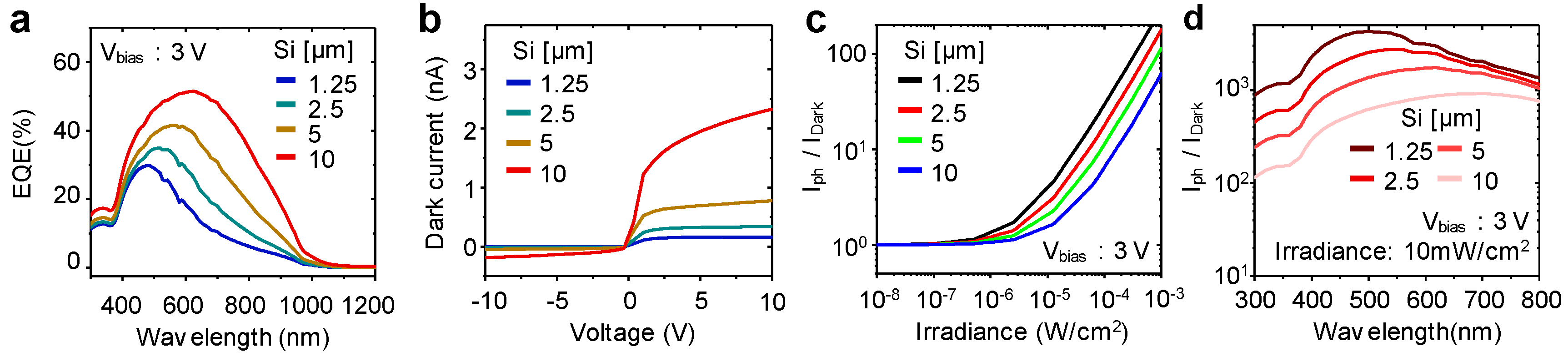
Figure 3.
(a) 3D scheme of lateral phototransistor and cross-sectional view; (b) conduction band profile with different doping concentrations and light intensity along the X direction at the cross-sectional line in Figure 3a; (c) recombination rate with three doping concentrations at the cross-sectional plane; (d) cumulative sum of recombination rate for different doping concentrations along the X direction; (e) photocurrent and dark current ratio for three impurity concentrations as a function of irradiance at a wavelength of 450 nm. The inset presents the I-V characteristics for each concentration at a wavelength of 450 nm and irradiance of 10 mW/cm2; (f) plot of I-V characteristics for inrinsic silicon having carrier concentration of 1014 cm−3 with different doping concentrations at a wavelength of 450 nm and irradiance of 10 mW/cm2.
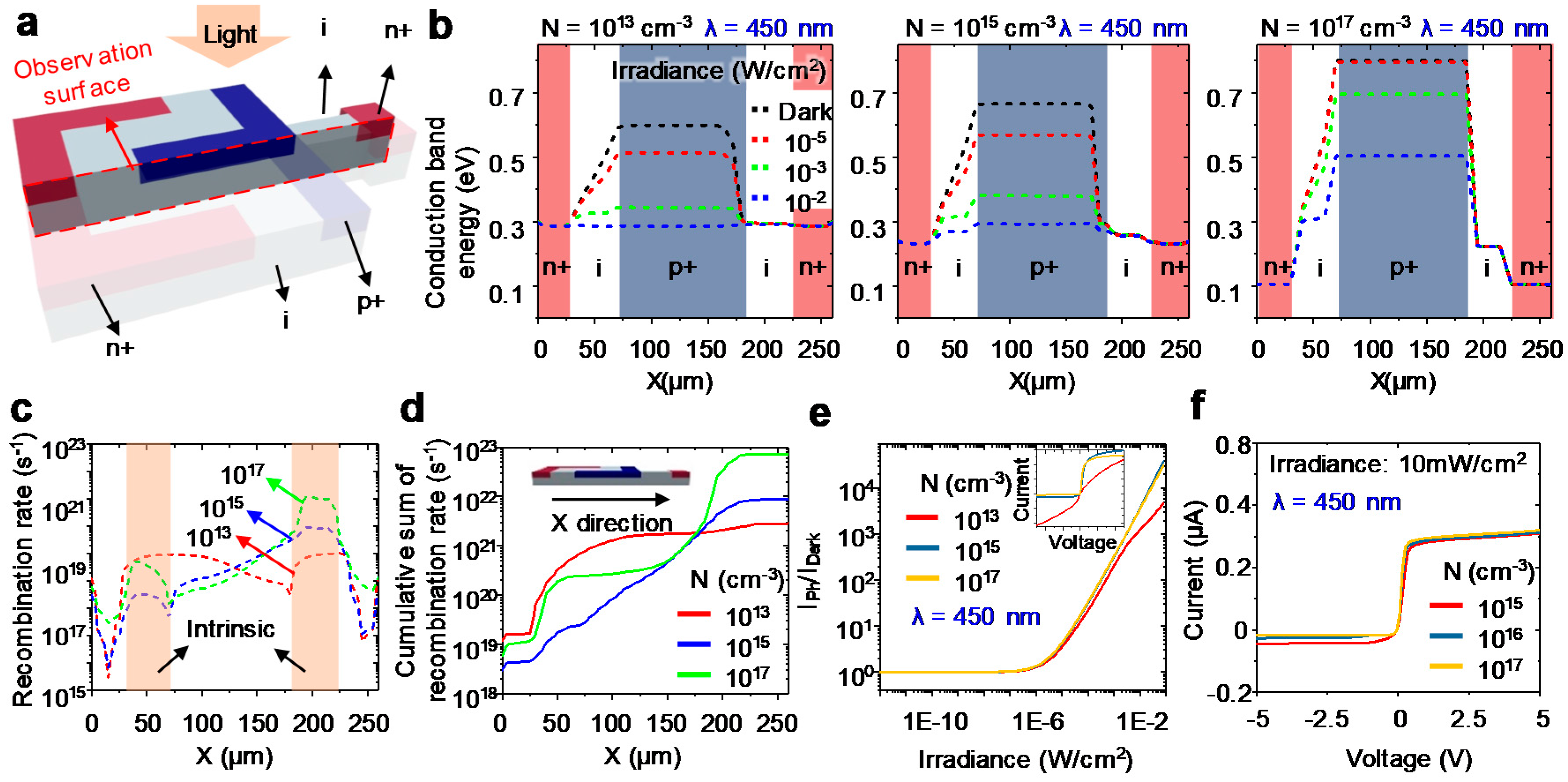
Figure 4.
Schematic illustrations of the fabrication process of the curved phototransistor array. (a) phototransistor devices; (b) etching for metallization process between each pixel; (c) Au/Cr electrode metallization; (d) polyimide (PI) encapsulation.
Figure 4.
Schematic illustrations of the fabrication process of the curved phototransistor array. (a) phototransistor devices; (b) etching for metallization process between each pixel; (c) Au/Cr electrode metallization; (d) polyimide (PI) encapsulation.

Figure 5.
(a) Schematic illustration of phototransistor array; (b) photograph and microscope image of the fabricated device and the picture on the right side is a magnified unit cell. The colored area indicates the doped regions; (c) scheme of phototransistor passive matrix with different numbers of rows. Inset shows the scheme of PTR array with 4 rows; (d) plot of current for single photodiode (PD) and PTR with various irradiances as a function of Voff at a wavelength of 450 nm; (e) Values of current in different phototransistor positions at Voff of 0V applied to the non-addressed rows in column A, as displayed in Figure 5c (Von = 3 V). Inset shows 2 by 2 passive matrix which has addressed and non-addressed pixels; (f) Plot of I-V curve for simulation and experimental measurement of PTR array.

Figure 6.
Four different phototransistors with a Si thickness of 1.25 μm and a doping concentration of 1015 cm−3: (a) rectangular NIPIN model; (b) small emitter NIPIN model; (c) rectangular NIPN model; (d) square NIPN model; (e–h) contour plots, which are positioned at the plane 50 nm from the surface, of recombination rate for each design; (i) total recombination rate and photogeneration rate for each model; (j) EQE for each model; (k) I-V characteristic at the wavelength of 450 nm and irradiance of 1 mW/cm2; (l) dark current characteristic as a function of Voff for each design.

Table 1.
Geometrical parameters for each design (Unit: μm).
| Model | L1 | L2 | L3 | L4 | L5 | L6 | D1 | D2 | D3 | D4 |
|---|---|---|---|---|---|---|---|---|---|---|
| Photodiode | 180 | 180 | 50 | 30 | - | - | 30 | 40 | 30 | 40 |
| Phototransistor | 180 | 180 | 50 | 30 | 30 | 50 | 30 | 40 | 30 | 40 |
Table 2.
Information of flexible/curved image sensors based on inorganic materials.
| Materials | Radius of Curvature | Deformability | Mechanism | Ref. |
|---|---|---|---|---|
| Si | 73 mm | Small | Thinning and bending | [8] |
| Si | ~19 mm | Small | Thinning and bending | [11] |
| Si | >15 mm | Cylindrical shape | Nanomembrane | [40] |
| Ge | 77.5 to 21 mm | Cylindrical shape | Nanomembrane | [41] |
| InGaAs | >2.5 mm | Cylindrical shape | Nanomembrane | [42] |
| Si | 28.5 mm | Cylindrical shape | Nanomembrane | [43] |
| Si | ~10 mm | Almost hemisphere | Photodetector array | [1] |
| Si | >11.4 mm | Almost hemisphere | Photodetector array | [3] |
| Si | ~6.96 mm | Hemisphere | Photodetector array | [2] 1 |
| Si | - | Hemisphere | Kirigami | [17] |
1 The photodetector array is the same structure with this research.
Table 3.
Geometrical parameters for each design (Unit: μm).
| Model | L1 | L2 | L3 | L4 | L5 | L6 | D1 | D2 | D3 | D4 | D5 | D6 |
|---|---|---|---|---|---|---|---|---|---|---|---|---|
| 1 | 180 | 180 | 50 | 30 | - | - | 30 | 40 | 30 | 40 | - | - |
| 2 | 180 | 180 | 50 | 30 | 30 | 50 | 30 | 40 | 30 | 40 | - | - |
| 3 | 180 | 180 | 30 | - | - | 30 | 30 | 40 | 30 | 40 | - | - |
| 4 | 180 | 180 | - | - | - | - | 30 | 40 | 30 | 40 | 25 | 30 |
© 2017 by the authors. Licensee MDPI, Basel, Switzerland. This article is an open access article distributed under the terms and conditions of the Creative Commons Attribution (CC BY) license (http://creativecommons.org/licenses/by/4.0/).
Share and Cite
MDPI and ACS Style
Kim, M.S.; Lee, G.J.; Kim, H.M.; Song, Y.M. Parametric Optimization of Lateral NIPIN Phototransistors for Flexible Image Sensors. Sensors 2017, 17, 1774. https://doi.org/10.3390/s17081774
AMA Style
Kim MS, Lee GJ, Kim HM, Song YM. Parametric Optimization of Lateral NIPIN Phototransistors for Flexible Image Sensors. Sensors. 2017; 17(8):1774. https://doi.org/10.3390/s17081774
Chicago/Turabian StyleKim, Min Seok, Gil Ju Lee, Hyun Myung Kim, and Young Min Song. 2017. "Parametric Optimization of Lateral NIPIN Phototransistors for Flexible Image Sensors" Sensors 17, no. 8: 1774. https://doi.org/10.3390/s17081774
Note that from the first issue of 2016, this journal uses article numbers instead of page numbers. See further details here.