Design Optimization and Fabrication of a Novel Structural SOI Piezoresistive Pressure Sensor with High Accuracy


E.T.S. Ingenieros Industriales, Polytechnical University of Madrid, C/José Gutiérrez Abascal, 2. 28006 Madrid, Spain
*
Author to whom correspondence should be addressed.
Sensors 2018, 18(2), 439; https://doi.org/10.3390/s18020439
Submission received: 9 January 2018
/
Revised: 30 January 2018
/
Accepted: 31 January 2018
/
Published: 2 February 2018
(This article belongs to the Special Issue Sensors for MEMS and Microsystems)
Abstract
:This paper presents a novel structural piezoresistive pressure sensor with four-grooved membrane combined with rood beam to measure low pressure. In this investigation, the design, optimization, fabrication, and measurements of the sensor are involved. By analyzing the stress distribution and deflection of sensitive elements using finite element method, a novel structure featuring high concentrated stress profile (HCSP) and locally stiffened membrane (LSM) is built. Curve fittings of the mechanical stress and deflection based on FEM simulation results are performed to establish the relationship between mechanical performance and structure dimension. A combination of FEM and curve fitting method is carried out to determine the structural dimensions. The optimized sensor chip is fabricated on a SOI wafer by traditional MEMS bulk-micromachining and anodic bonding technology. When the applied pressure is 1 psi, the sensor achieves a sensitivity of 30.9 mV/V/psi, a pressure nonlinearity of 0.21% FSS and an accuracy of 0.30%, and thereby the contradiction between sensitivity and linearity is alleviated. In terms of size, accuracy and high temperature characteristic, the proposed sensor is a proper choice for measuring pressure of less than 1 psi.
Keywords:
piezoresistive pressure sensor; high sensitivity; low pressure nonlinearity error; SOI structure; micro-pressure measurementPACS:
J01011. Introduction
The phenomenon by which the electrical resistance of a material changes in response to mechanical stress is known as piezoresistivity. Piezoresistivity in semiconductor is widely applied in different sensors including pressure sensors, accelerometers, cantilever force sensors, and inertial sensors [1]. Piezoresistive pressure sensors utilize piezoresistive effect as the detection mechanism. A Wheatstone bridge is built through electric connections with four piezoresistors to transduce the resistance change into output voltage when pressure is applied on the membrane surface. Owing to their small scale, easy integration, direct signal transduction mechanism, etc. [2], piezoresistive pressure sensors have been most commonly used in automobile [3], aerospace [4,5] and petrochemical [6] fields for pressure measurements.
For many years in the past, monocrystalline silicon strain gauges have been mainly chosen as the detection elements in pressure sensors. Their main characteristics include good sensitivity, high mechanical stability and batch fabrication capability owing to the single crystal structure [7,8]. For such traditional type of sensors, the p-n junction formed by the resistor with the bulk plays a main role in isolation of the resistors from substrate. However, once the temperature exceeds 125 °C, there exists serious degradation in the performance of the sensor due to leakage currents [9]. To solve this problem, some wide band gap semiconductors such as SiC and diamond have been explored as alternatives, but their microfabrication process is not mature enough [10,11]. Polysilicon can also be a viable candidate at high temperature because of an isolating oxide layer under the polysilicon resistor. However, some undesirable characteristics, such as low sensitivity, high noise, and repeatability problems, limit its further development [12,13].
By considering the working condition, the device should maintain their functionalities even at high temperatures. SOI (silicon on insulator) stands out as the most promising candidate. The fabrication of the SOI wafer has been generically described as the bonded wafer approach. As the name implies, two wafers are bonded together by thermally grown silicon oxide (SiO2) [14]. This structure solves many drawbacks, such as sensibility to radiation, current leakage and instability at high temperature. Thus, SOI allows piezoresistive pressure sensors to work at an operating temperature range up to 300 °C [15,16]. Besides, SOI piezoresistive pressure sensors give the combined advantages of standard silicon technology and isolation of piezoresistors from substrate, which makes SOI one of the best recognized and promoted material for piezoresistive pressure sensors [17].
For conventional structural pressure sensors, the trade-off between sensitivity and linearity is always irreconcilable, especially in the field of low pressure measurements [18]. Since sensitivity is proportional to the ratio (membrane length)/(membrane thickness), namely (L/H). Unfortunately, the nonlinearity increases with this ratio at a faster rate, as the nonlinearity of the pressure-to-stress conversion is proportional to (L/H)4 [19]. However, both sensitivity and linearity are important performance indicators, which may directly determine consumer satisfaction degree and market share. To achieve a higher sensitivity and alleviate the contradiction between the sensitivity and linearity simultaneously, many novel structurally sensitive membranes, such as E-type membrane [20], hollow reinforced membrane [21], circular grooved membrane [22], peninsula structural membrane [23], cross-beam membrane (CBM) [24], beam-membrane-mono-island (BMMI) [25], beam-membrane-dual-island (BMDI) [26], beam-membrane-quad-island (BMQI) [27], etc., were developed in the past decades. By comparing and analyzing such novel structures, it is found they have some common features. Either they create stress concentration regions (SCRs) and localize more strain energy within a relatively narrow space, or they locally stiffen the membrane thereby restricting partially the deformation but not affecting the stress concentration in the sensitive areas. Just because of the formation of stress concentration and locally stiffened membrane, the sensitivity and linearity both achieve a big improvement.
In this paper, a novel structural piezoresistive pressure sensor with four-grooved membrane combined with rood beam was proposed for low pressure measurement (0~1 psi) based on SOI substrate. By choosing SOI as the sensor chip, a good high temperature performance was desired. By introducing the grooves and rood beam to sensitive membrane, a high sensitivity and a low nonlinearity error were anticipated to be achieved simultaneously. To optimize the structural dimensions, the finite element method (FEM) and the nonlinear curve fitting method were implemented. Based on the optimization results, the proposed structure was fabricated as the sensor chip, which was assembled to form a pressure sensor. Finally, experiments were carried out to evaluate the performance.
2. Structure Design and Simulation
2.1. Structure Design
In this paper, a novel structure featuring four-grooved membrane combined with rood beam was designed for the sensor chip to measure low pressure of less than 1 psi. A 4 inch n-type (100) oriented SOI wafer with 30 μm top silicon, 2 μm buried SiO2 layer and 300 μm bottom silicon was chosen as substrate.
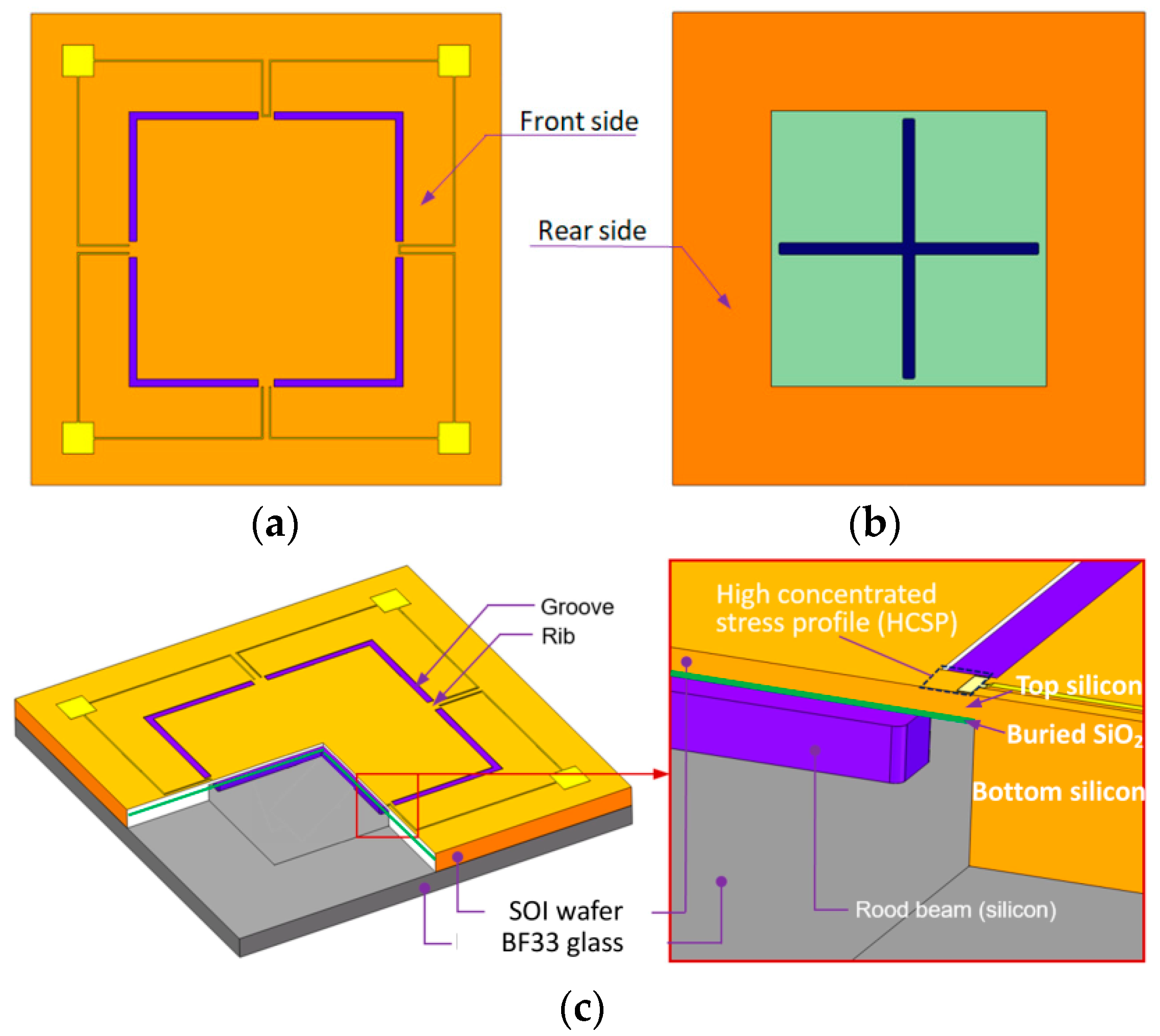
On the front side, there are four bending grooves on the membrane surface as shown in Figure 1a. Moreover, four ribs are located between every two grooves which are just on the top of the gap between each beam and membrane edge. Then, a Wheatstone bridge is built up through electric connections with the four piezoresistors on the surface of the rib regions.
On the rear side, a rood beam structure is placed as shown in Figure 1b. The end of each rood beam is not connected with membrane edge but remains at a distance between them, which can be seen clearly in Figure 1c. Meanwhile, the rib width is equal to the groove width, and the rib length is equal to the rood beam width, which not only simplifies the fabrication processes, but facilitates the dimension variables optimization. By incorporating four grooves and a rood beam into the membrane, a high concentrated stress profile (HCSP) was anticipated to maximize the sensitivity. Meanwhile, a locally stiffened membrane (LSM) structure was anticipated to be generated to decrease the deflection of the plate but not reduce the stress around the HCSP.
2.2. Mechanical Simulation
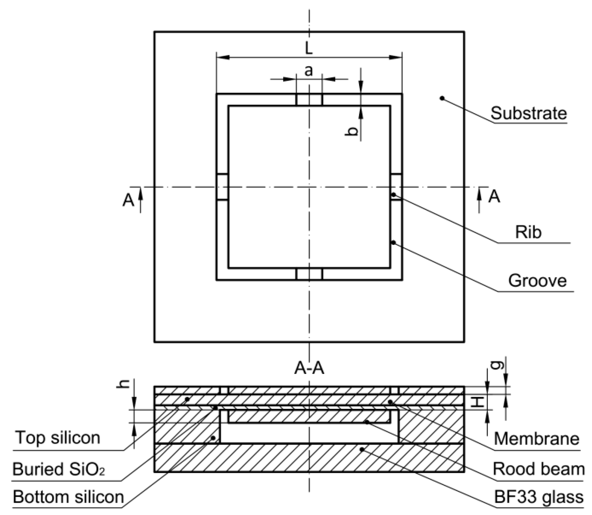
To better display the geometry of the structure, the front view and cross-sectional view along A-A of the proposed chip are presented in Figure 2, marked with structural dimension variables. L is the membrane length, H is the membrane thickness, b is the groove width, g is the groove depth, and a and h are rood beam width and thickness, respectively. Meanwhile, the bonding BF33 glass on the rear side can be found obviously from the cross-sectional view. Based on the previous design experiences [7,9,14], the scope for each structural dimension variable is followed by:
In the scope for each structural dimension variable, take some fixed size as an example. The stress of the proposed membrane is calculated under 1 psi by non-linear static analysis and model analysis using the commercially-available FEM software COMSOL Multiphysics®. Only a quarter of the model is established for the sensitive membrane due to the symmetry as shown in Figure 3a. It can be found that the stress is mainly concentrated at the hinge area which is located at the rib surface, as displayed by the dotted square, which is indicated as HCSP. For P-type [110] oriented piezoresistors, the sensitivity is actually determined by the magnitude of the difference between the transversal stress σx and the longitudinal stress σy, namely, σ = σx − σy. It can be seen that the maximum stress along x-path appears at HCSP, but the stress in other regions of membrane is close to zero, as shown in Figure 3b. It illustrates that the strain energy is strictly limited in a narrow area and the energy is not spread easily outside the HCSP. There is a small distance between the rood beam and edge on the back side of the membrane. This gap is used to form a stiffness mutation, which can further enhance the stress concentration. Then, the resistors can experience more stresses and strains, the sensitivity will be improved again.
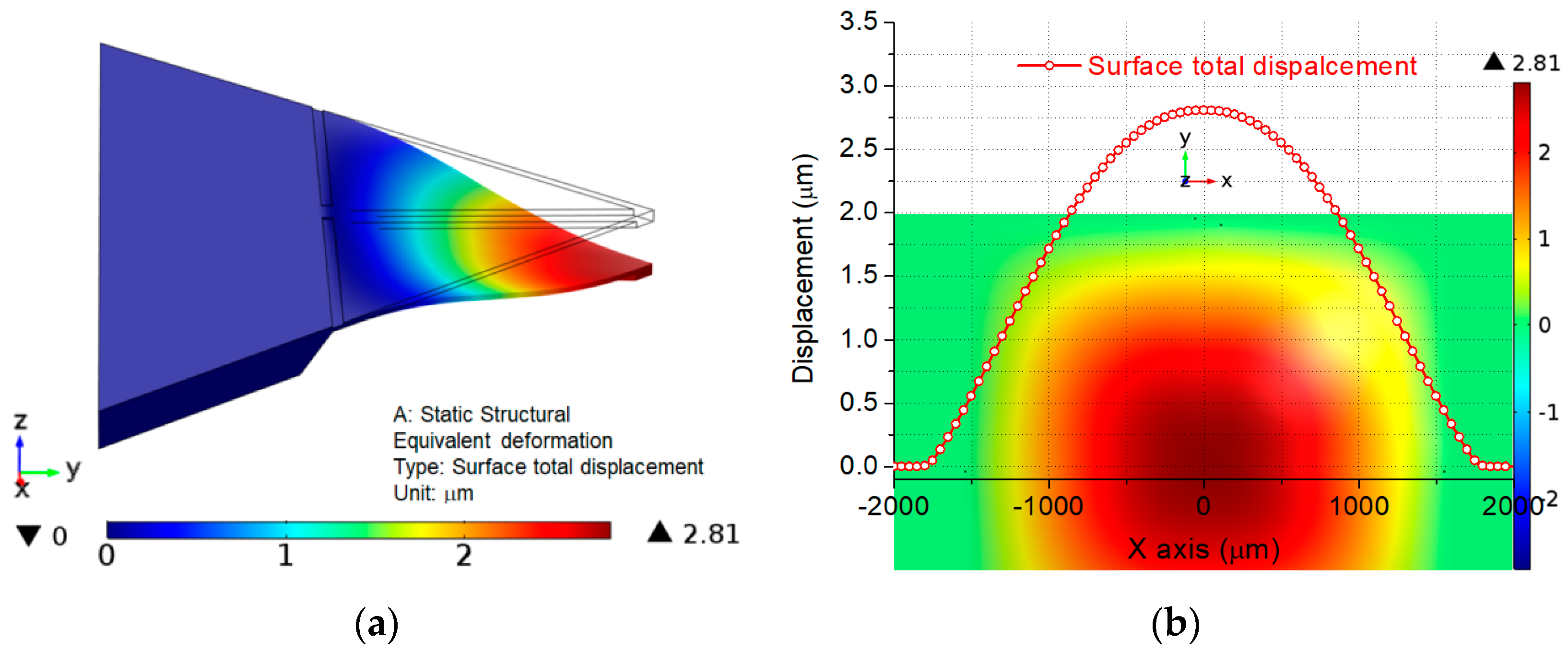
According to the ratio between membrane deformation and thickness, the deflection theory can be divided into small-deflection theory and large-deflection theory. Small-deflection theory is always chosen to describe the principle of the sensor but large-deflection theory is usually adopted to illustrate the phenomenon of nonlinearity error. Once the deflection exceeds the definite value compared to the thickness of the membrane, the large deflection theory works, and, then, linearity between deflection and pressure will change to nonlinearity [28]. Based on the large deflection curve, the relationship between pressure and deflection is no longer linear when the ratio of (membrane deflection)/(membrane thickness) is larger than 0.2 [29]. It indicates the small-deflection theory only works when the deflection is smaller than 1/5 of the membrane thickness. Thus, the maximum deflection should be less than 1/5 of the membrane thickness, which is beneficial for obtaining a low pressure nonlinearity error. The simulation of surface displacement only displays a 1/4 model of the membrane because of the symmetry. The maximum surface displacement appears at the center of the membrane as shown in Figure 4a. The maximum displacement value reaches 2.8 μm, which is almost 1/10 of the membrane thickness (30 μm), as shown in Figure 4b, and totally satisfies the principle of small-deflection theory.
2.3. Geometry Optimization
To determine the geometry of the sensitive membrane, the relationship between the dimension variables and mechanical performance should be discussed. In this section, a combination of FEM simulation and curve fitting method is chosen to deduce the theoretical formulas of the proposed membrane.
Based on the formulas of traditional C-type membrane, the maximum stress and deflection of the membrane are the power functions of each single structural dimension variable [30,31]. In theory, the formulas for the proposed structure should be similar to C-type. Consequently, the functional forms are followed by:
where L, H, h, a, b, and g are the structural dimensions as shown in Figure 2; P and E are the applied pressure and Young’s elastic modulus, respectively; σmax, ωmax and σoverload are the maximum von Mises stress, maximum deflection, and maximum von Mises stress under a fixed pressure (100 psi), respectively; and Q1, Q2, Q3, c1, c2, d1, d2, d3, i1, i2, i3, k1, k2, k3, m1, m2, m3, n1, n2, n3, r1, r2, r3, s1, s2, and s3 are the curve fitting coefficients.
To calculate above coefficients, each single dimension variable should be discussed separately. For instance, when membrane length L is discussed, other variables have to be assumed as constants. The values of these variables are given initially and arbitrarily in the ranges of actual microfabrication. Thus, Equations (1)–(3) can be simplified to:
where Q1l, Q2l and Q3l are the coefficients for the variable L, and other parameters have been mentioned. Since the variation of the membrane length L, a series of σmax, ωmax and σoverload will be obtained by FEM numerical calculation. Then, fitting curves and the coefficients Q1l, Q2l, Q3l, i1, i2, and i3 are obtained by utilizing the software Origin in accordance with simulation results. Then, Equations (4)–(6) are followed by:
Using the same approach, the fitting equations and curves related to other membrane dimensions can also be deduced. Then, equations about membrane thickness H are derived as:
In addition, the equations related to groove width b are shown as:
According to Equation (15), it can be concluded that groove width b has little influence on the σoverload. Moreover, the equations with respect to groove depth g are listed as:
For rood beam width a, the relative equations are followed by:
In the same way, the equations regarding rood beam thickness h are:
Equation (24) reveals that there is tiny impact of the rood beam thickness h on the σoverload. The equations about pressure P are followed by:
From Equations (25) and (26), the stress and deflection of the membrane show linear relationships with the pressure P. Finally, the equations related to Young’s elastic modulus E are expressed as follows:
Equations (27)–(29) not only illustrate that the Young’s elastic modulus E has almost no effect on σmax and σoverload, but also reveal the inverse proportional relationship between E and maximum deflection ωmax. By combining all the equations related to each single variable, the particular equations of Equations (1)–(3) can be determined. Simultaneously, to calculate the constant coefficients Q1, Q2, and Q3, a set of particular solutions are introduced, and thus the relative main equations can be derived as follows:
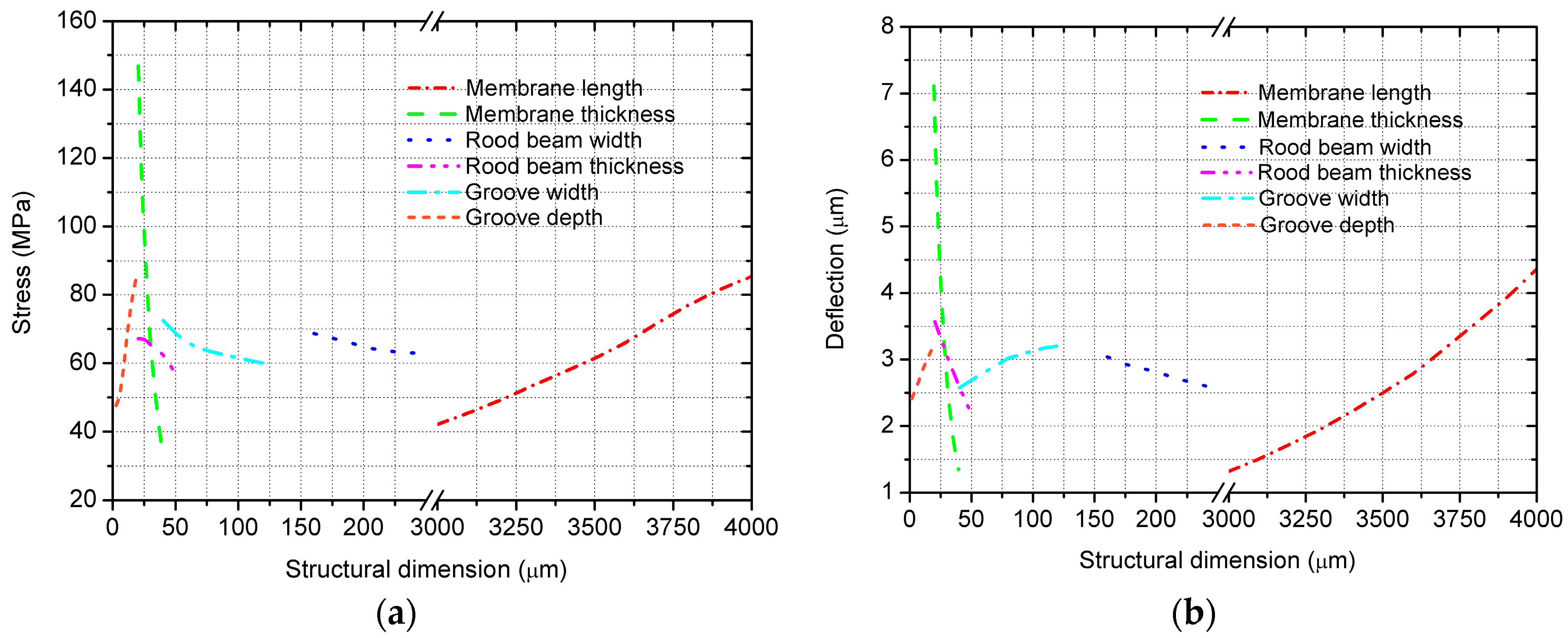
From Equations (30)–(32), it can be found that with the increase of the membrane length L, the maximum stress and deflection, both, experience a rise, namely, improve sensitivity, but worsen linearity. Meanwhile, the impacts for the membrane thickness H, rood beam thickness h, rood beam width a and groove depth g on the sensitivity and linearity are same except groove width b. It is the only variable which is inversely proportional to the stress and directly proportional to the deflection. It means that the sensitivity and linearity can be improved synchronously when the groove width is chosen appropriately. Besides, groove width b and rood beam thickness h have nearly no influences on σoverload.
The impacts of structural dimension variables on the stress and deflection variations are presented in Figure 5a,b. To determine the optimal solution of the nonlinear optimization problem, MATLAB is used. By the fine adjustment of the MATLAB calculated results, a series of structural dimensions are finally determined based on comprehensively regarding the influences on stress and deflection of the membrane as listed in Table 1.
3. Fabrication and Measurements
A 4-inch (100 ± 0.5 mm) n-type SOI wafer oriented in the (100) direction with a resistivity of 10 Ω·cm was chosen as the substrate of the sensor chip. It is 330 ± 5 μm thickness and double sides polished with a total thickness variation of less than 5 μm. The specific fabrication process of the proposed sensor chip is summarized as follows. The first step is to grow SiO2 protective layers on both sides of the wafer by thermal oxidation. A 300 ± 20 nm SiO2 deposition layer is formed using wet oxidation at 1000 °C. Then, lithography is performed on the front side of silicon oxide to pattern the piezoresistors. The front side of wafer is implanted with boron ions (dose 4.86 × 10¹⁴ atoms/cm2, energy 70 keV) and subsequently annealed at 1000 °C for 30 min in N2 ambient for dopant activation. P-type resistors (210 ± 10 Ω/Sq.) and heavy doping of contact regions are formed in the doped region. After that, the low pressure chemical vapor deposition (LPCVD) is adopted to grow the passivation layers of Si3N4 to protect the piezoresistors. Subsequently, the reactive ion etching (RIE) process is used to etch the ohm contact regions between the piezoresistors and the metal lead. Next, Cr/Au (50 nm/200 nm) coatings are deposited and patterned for the purpose of connecting of resistors and forming of bonding pads as presented in Figure 6a. In the following, RIE is applied to create four grooves on the front side, and DRIE is used to form the cavity and rood beam on the rear side. Moreover, it is noteworthy that the rear side etching is processed in two steps. The first step is to etch rood beam patterning by one mask (etching depth was 35 μm). The second step is to form the cavity and rood beam structure simultaneously by another mask. To obtain an absolute pressure reference chamber, the bottom side of the wafer is attached to the BF33 glass by anodic bonding process under vacuum condition (5 × 10⁻⁶ Bar) at 360 °C with an electric field of 600 V (20 min). The photographs of the sensor chip after laser cutting are shown in Figure 6b.
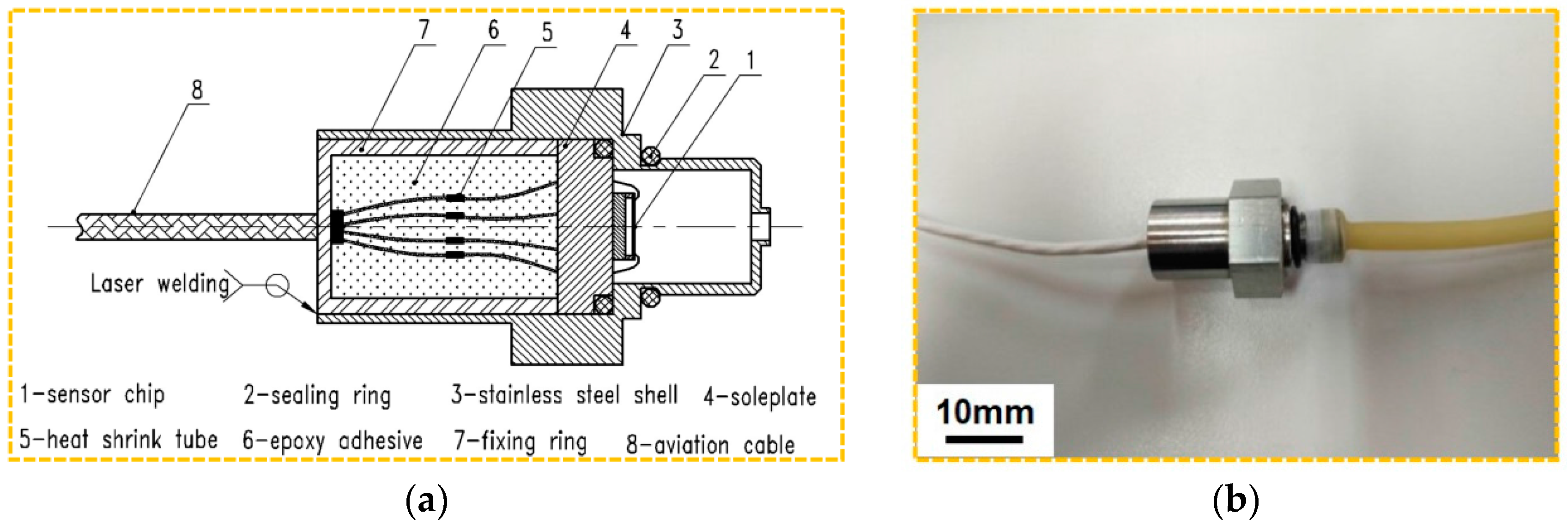
The pressure sensor is assembled with the fabricated sensor chip as shown in Figure 7a. The sensor is mainly constituted by chip, shell, soleplate, aviation cable, etc. The metal material of the external structure is 304 stainless steel which is beneficial to improve the corrosion resistance. To increase the sealing and insulation characteristics of the sensor, the epoxy adhesive (60% ethoxyline resin, 30% quartz powder, 10% dioctyl phthalate) is filled in the shell and solidified for about 24 h at room temperature (25 °C). An aviation cable is used to connect the sensor and the plug, which can resist high temperatures (>200 °C). To protect the welding spot, the fluororubber heat shrink tube is covered at the connection between every two wires. Between the stainless steel shell and fixing ring, laser welding is chosen for connection, which can improve the long term stability and application of the sensor. As a result, the assembled sensor is presented in Figure 7b.
The performances of the sensor are measured and the experimental schematic diagrams for testing are shown in Figure 8. The bridge resistance is measured by a digital multimeter (VC890D). The pressure is from a pressure pump and the pressure value can be adjusted by controlling switch. To ensure the airtightness of the measurement, the joint between the sensor port and connecting tube should be twined several laps using the rubber belt. A constant voltage of 5 V is provided to the Wheatstone bridge of the sensor using a High Current Switching DC Power Supplier (Model BK1694). The output of the sensor at different pressure loads is read by a digital multimeter (FLUKE 8845A). The output voltages at different temperatures are measured in a high and low temperature test chamber (GDC4010) with the working range of −20 to 150 °C. To test the characteristics of the sensor at different temperatures, nine temperature points are tested in the range of −20 to 150 °C: −20 °C, −10 °C, 0 °C, 25 °C, 50 °C, 75 °C, 100 °C, 125 °C and 150 °C. The purpose is to check the temperature characteristic of the device. In the process of high temperature measurement, the test step change of pressure is set as 0.1 psi, namely, a total number of eleven test points is selected. Based on the pressure sensor calibration procedures, the pressure signals increase from low to high until 1 psi, and then decrease from 1 psi to 0. The above process is called “one trip”. For each temperature point, three trips are carried out for a precise measurement. For each test point in each trip, the output data will be not read until the pressure is stable. Finally, the various indicators of the sensor are calculated.
4. Results and Discussion
After assembling the sensor, the first step is to connect the plug and socket to measure the bridge resistance. The resistances of three samples are listed in Table 2. Test results show that the consistency of the resistance is not high enough. This is mainly because the connecting regions between piezoresistors and Cr-Au wires have some different degrees of the defects. Besides, most of the measured resistances are smaller than the designed value 6.7 kΩ. This is due to the errors involved in ion implantation and sputtering processes. The resistance of Device 2 is the closest to the design value, so it is chosen as the sample to be tested at different conditions.
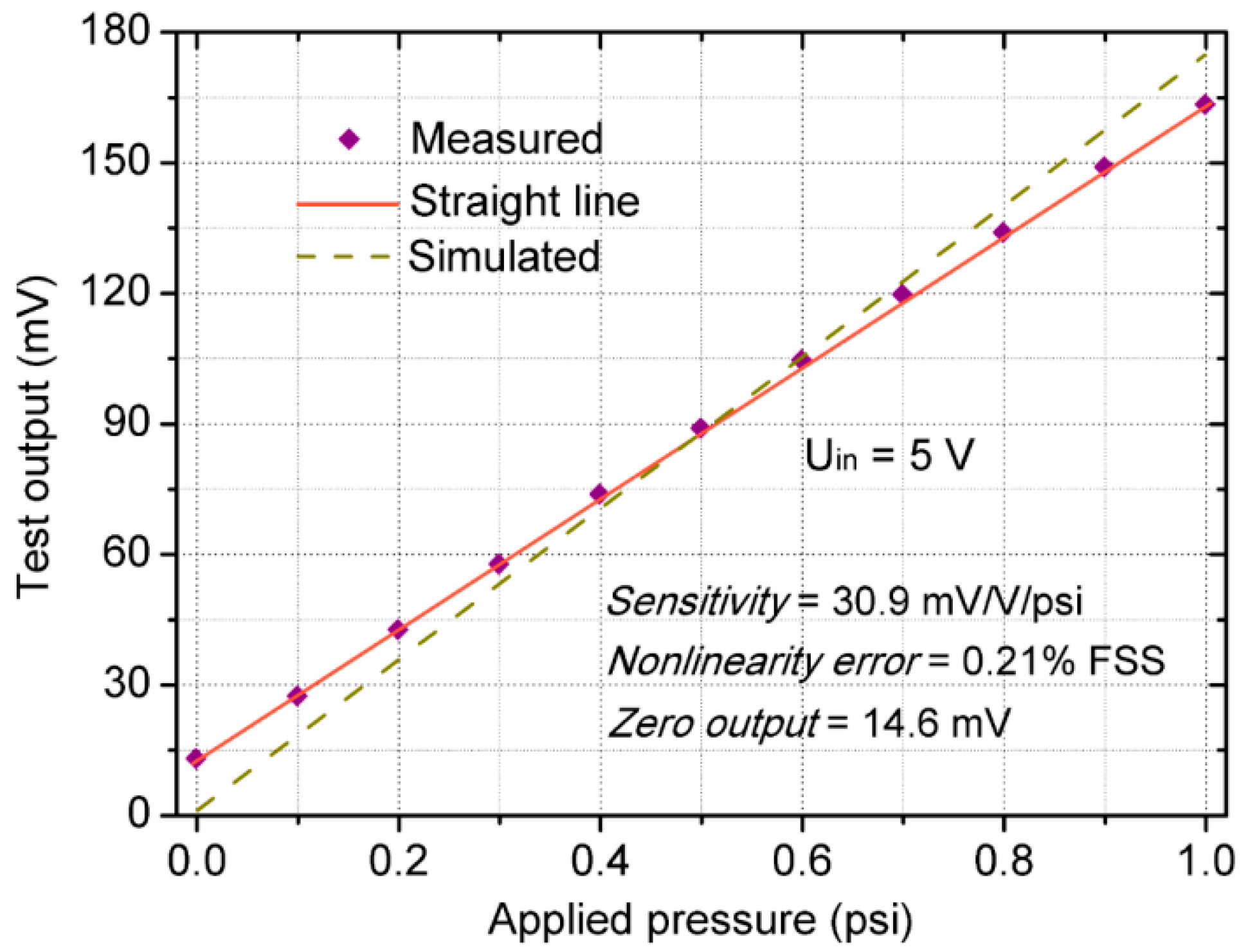
The performance of one pressure sensor is usually evaluated by the static characteristics of technical indicators including full scale output, sensitivity, pressure nonlinearity error, repeatability, hysteresis, zero output, accuracy, etc. [32]. The measured output voltage and pressure nonlinearity error are shown in Figure 9. In this paper, the accuracy is calculated using root of the sum squared to combine nonlinearity, repeatability, and hysteresis into a total accuracy percentage. Finally, the detailed technical data of the sensor at room temperature (25 °C) are listed in Table 3. The results illustrate that the proposed sensor achieves a high sensitivity of 30.9 mV/V/psi and a low nonlinearity error of 0.21% FSS (full scale span). Meanwhile, there is a deviation of 8.4% between the simulated and experimental results. It is illustrated that the estimated data are similar to the actual data, which proves the validity of the simulation and optimization methods.
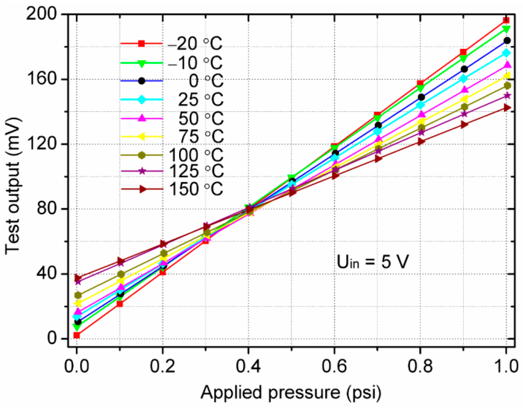
The sensitivity and zero output analyses are the study of change in output voltage with respect to the applied pressure at different temperatures. Figure 10 illustrates the relationship between the output of the sensor and the standard pressure under different temperatures. It can be observed that the lower the temperature is, the larger the output voltage is. It is also observed that the output increases linearly with the applied pressure. However, the output curves of the sensor at different temperatures are not coincident and there are also differences in the zero output voltage as well as the sensitivity, which demonstrates that the proposed sensor has a temperature drift. It is consistent with the conclusion of References [33,34].
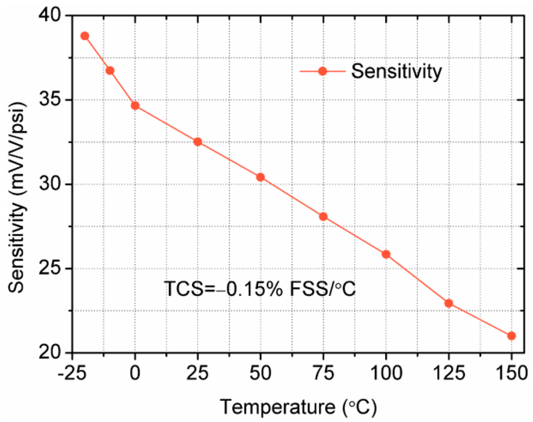
To be more intuitional, Figure 11 displays the sensor’s sensitivity changes with the temperature increasing when the test pressure is 1 psi. The results show that the sensitivity reduces almost by 50% when the temperature increases from −25 °C to 150 °C. This is mainly because the piezoresistive coefficient decreases when the temperature rises. However, the sensitivity is still as high as 21.2 mV/V/psi at 150 °C. The temperature coefficient of sensitivity (TCS) is calculated using the full output at 150 °C and reference temperature 25 °C, where the TCS of the sensor is −0.15% FSS/°C, indicating that the sensitivity of the sensor has a negative temperature coefficient.
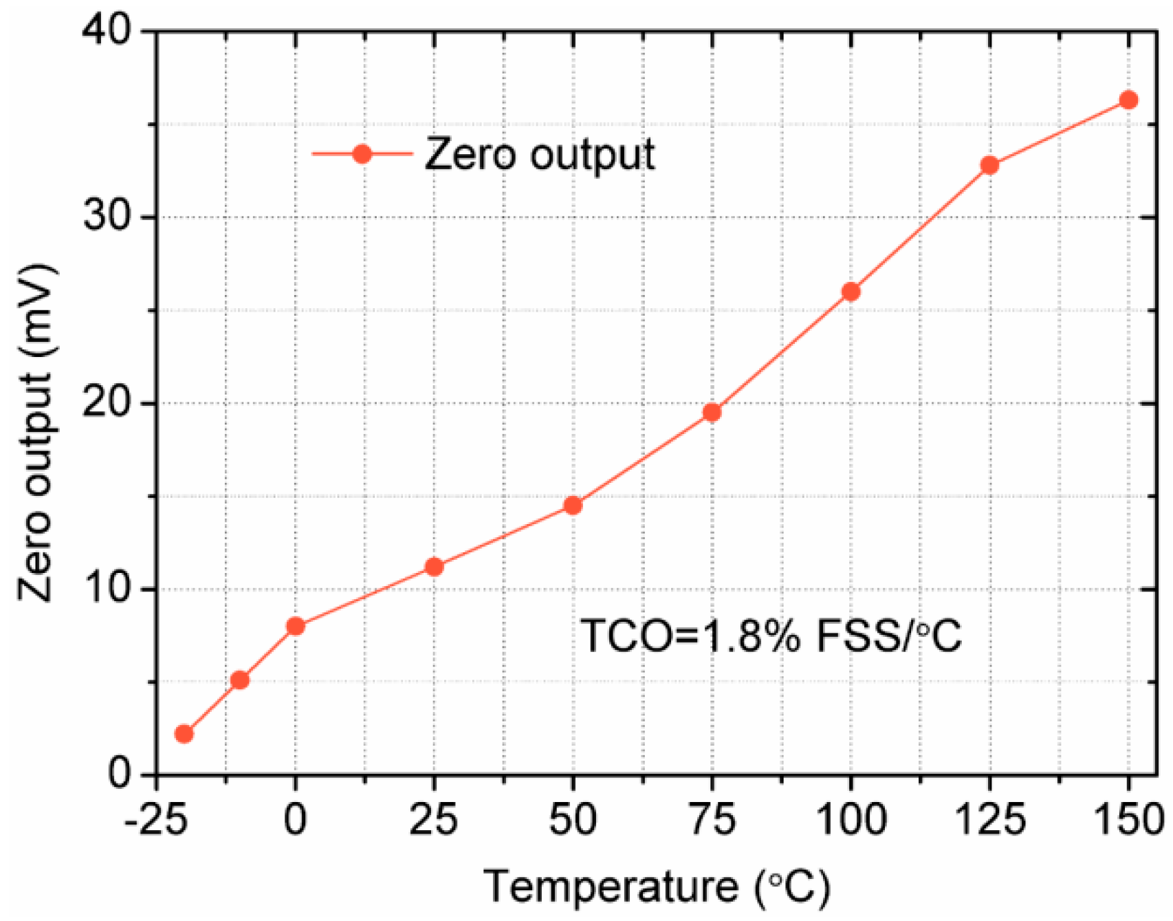
The zero output voltage increases substantially when the temperature is rising, as shown in Figure 12. The zero output comes from two aspects. The first reason is due to some residual stress on the membrane. The second reason is because of the non-uniformity in the doping of the four piezoresistors. The high value of zero output at high temperature may be attributed to the difference in the shapes of piezoresistors experiencing longitudinal and transverse stresses [35]. It is found that the zero output increases 15.5 times when the temperature is changing from −20 °C to 150 °C, which indicates the proposed sensor possesses an obvious temperature-sensitive character. By calculation, the temperature coefficient of voltage offset (TCO) of the sensor is 1.8% FSS/°C.
Generally, two methods are usually adopted to reduce offset voltage. On the one hand, the piezoresistive coefficients are the function of the temperature and doping concentration, namely, π(N,T) = π0 × P(N,T). According to the piezoresistance factor influenced by the temperature and impurity concentration for monocrystalline silicon, a lower doping concentration is commonly needed [36]. On the other hand, the offset voltage can also be decreased by incorporating compensation circuits and signal-conditioning circuits either by using them on the silicon die itself or by employing hybrid components/signal conditioning ICs/resistor.
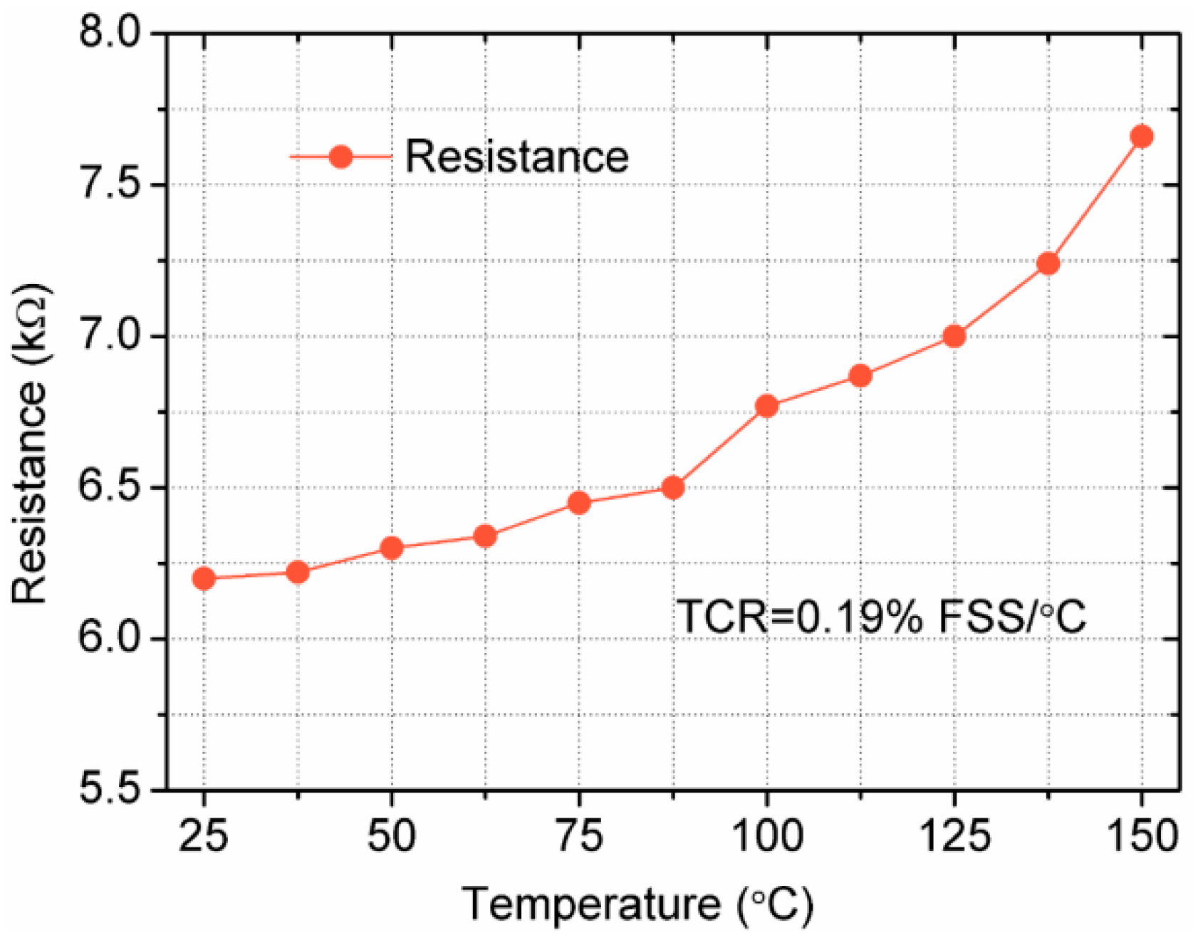
With the temperature increases, the resistance experiences a rise until reaching the largest value at 150 °C, as shown in Figure 13. Commonly, one requirement of analog electronics is the positive temperature coefficient of the sensitivity over the entire temperature range. Thus, the positive temperature coefficient of resistivity (TCR) has to predominate the negative temperature coefficient of the gauge factor [37]. Based on the resistance variation, TCR is calculated as 0.19% FSS/°C.
The proposed sensor demonstrates that it does have the ability to alleviate the contradiction between sensitivity and linearity to realize the micro measurement with high accuracy, as shown in Table 4. Compared with the four other reported sensors, the sensitivity of the proposed sensor is the second largest, which is more than three times larger than that reported in [38]. At the same time, the pressure nonlinearity for the sensor is intermediate among the five types of sensors, unlike [39] where the small pressure nonlinearity is obtained but its sensitivity is too low. Thus, it can be concluded that the proposed sensor achieves a high sensitivity and a low pressure nonlinearity error when compared with the reported sensors. The proposed sensor not only achieves a good performance by nonlinear optimization of the structure, but also obtains a good output characteristic at high temperature using SOI as the substrate. In other words, the sensor in this work is the only candidate that can work in high temperature, when compared to the four other reported devices.
Based on the measurement at different temperatures, the temperature characteristic for the proposed sensor is illustrated. The sensitivity is 21.2 mV/V/psi, the nonlinearity is 0.25% FSS, the repeatability is 0.19% FSS, the hysteresis is 0.13% FSS, and so the accuracy is up to 0.34% FSS. Obviously, the sensor also satisfies the linearity at high temperature. As the temperature is rising, the characteristic has some degradation, but, overall, the change in accuracy is not obvious. The sensor maintains fine characteristic at high temperature. The contrast in accuracy between the proposed sensor and several previously reported sensors is displayed in Table 5. Compared with the other reported sensors, the proposed sensor achieves the best linearity. Moreover, the accuracy for the sensor is intermediate among the four sensors. Therefore, it can be concluded that the proposed sensor achieves a high accuracy at high temperature when it is compared with several reported sensors.
5. Conclusions
In this study, a novel structural piezoresistive pressure sensor was developed by introducing a rood beam into a four-grooved membrane. The proposed structure provided a solution for enhancing sensitivity and linearity simultaneously. To testify the feasibility of the scheme, the proposed model was simulated, optimized, fabricated and measured. Test results illustrated the effectiveness of incorporating grooves and a rood beam to improve accuracy and alleviate the trade-off between sensitivity and linearity. Besides, the fabricated pressure sensor exhibited high linearity and accuracy at high temperature. Thus, in terms of micro size, accuracy and high temperature characteristic, the proposed structure was a good candidate for measuring low pressure in the range of 0–1 psi under 150 °C.
Acknowledgments
The work was supported by the China Scholarship Council (CSC) for studying abroad (201508320275) and Erasmus+ project (2015-1-ES01-KA107-015460). We would also like to thank for the help in microfabrication the Key Laboratory of Micro/Nano Systems for Aerospace, Northwestern Polytechnical University and Suzhou Institute of Nano-Tech and Nano-Bionics (SINANO), Chinese Academy of Sciences.
Author Contributions
The work in this paper was a collaboration of all authors. Chuang Li carried out the design, FEM analysis and fabrications process, as well as the wrote the manuscript. Francisco Cordovilla designed and performed the simulation process. R. Jagdheesh gave valuable suggestions for the discussion part and helped with the revision of the manuscript. José L. Ocaña conceived and designed the model, and guided the optimization of parameters and the article structure.
Conflicts of Interest
The authors declare no conflict of interest.
References
- Barlian, A.A.; Park, W.T.; Mallon, J.R.; Rastegar, A.J.; Pruitt, B.L. Review: Semiconductor piezoresistance for microsystems. Proc. IEEE 2009, 97, 513–552. [Google Scholar] [CrossRef] [PubMed]
- Khodasevych, I.; Parmar, S.; Troynikov, O. Flexible sensors for pressure therapy: Effect of substrate curvature and stiffness on sensor performance. Sensors 2017, 17, 2399. [Google Scholar] [CrossRef] [PubMed]
- Gradolph, C.; Friedberger, A.; Müller, G.; Wilde, J. Impact of high-g and high vibration environments on piezoresistive pressure sensor performance. Sens. Actuators A Phys. 2009, 150, 69–77. [Google Scholar] [CrossRef]
- Moghaddam, M.K.; Breede, A.; Brauner, C.; Lang, W. Embedding piezoresistive pressure sensors to obtain online pressure profiles inside fiber composite laminates. Sensors 2015, 15, 7499–7511. [Google Scholar] [CrossRef] [PubMed]
- Zhou, G.; Zhao, Y.; Guo, F.; Xu, W. A smart high accuracy silicon piezoresistive pressure sensor temperature compensation system. Sensors 2014, 14, 12174–12190. [Google Scholar] [CrossRef] [PubMed]
- Niu, Z.; Zhao, Y.; Tian, B. Design optimization of high pressure and high temperature piezoresistive pressure sensor for high sensitivity. Rev. Sci. Instrum. 2014, 85, 015001. [Google Scholar] [CrossRef] [PubMed]
- Tian, B.; Zhao, Y.; Jiang, Z.; Zhang, L.; Liao, N.; Liu, Y.; Meng, C. Fabrication and structural design of micro pressure sensors for Tire Pressure Measurement Systems (TPMS). Sensors 2009, 9, 1382–1393. [Google Scholar] [CrossRef] [PubMed]
- Li, X.; Liu, Q.; Pang, S.; Xu, K.; Tang, H.; Sun, C. High-temperature piezoresistive pressure sensor based on implantation of oxygen into silicon wafer. Sens. Actuators A Phys. 2012, 179, 277–282. [Google Scholar] [CrossRef]
- Zhao, Y.L.; Zhao, L.B.; Jiang, Z.D. High temperature and frequency pressure sensor based on silicon-on-insulator layers. Meas. Sci. Technol. 2006, 17, 519–523. [Google Scholar] [CrossRef]
- Fragaa, M.A.; Furlan, H.; Massia, M.; Oliveiraa, I.C.; Koberstein, L.L. Fabrication and characterization of a SiC/SiO2/Si piezoresistive pressure sensor. Procedia Eng. 2010, 5, 609–612. [Google Scholar] [CrossRef]
- Kulha, P.; Babchenko, O.; Kromka, A.; Husak, M.; Haenen, K. Design and fabrication of piezoresistive strain gauges based on nanocrystalline diamond layers. Vacuum 2012, 86, 689–692. [Google Scholar] [CrossRef]
- Shi, C.; Liu, X.; Chuai, R. Piezoresistive sensitivity, linearity and resistance time drift of polysilicon nanofilms with different deposition temperatures. Sensors 2009, 9, 1141–1166. [Google Scholar] [CrossRef] [PubMed]
- Singh, K.; Joyce, R.; Varghese, S.; Akhtar, J. Fabrication of electron beam physical vapor deposited polysilicon piezoresistive MEMS pressure sensor. Sens. Actuators A Phys. 2015, 223, 151–158. [Google Scholar] [CrossRef]
- Zhao, X.; Li, D.; Yu, Y.; Wen, D. Temperature characteristics research of SOI pressure sensor based on asymmetric base region transistor. J. Semicond. 2017, 38, 074008. [Google Scholar] [CrossRef]
- Yao, Z.; Liang, T.; Jia, P.; Hong, Y.; Qi, L.; Lei, C.; Zhang, B.; Xiong, J. A high-temperature piezoresistive pressure sensor with an integrated signal-conditioning circuit. Sensors 2016, 16, 913. [Google Scholar] [CrossRef] [PubMed]
- Giuliani, A.; Drera, L.; Arancio, D.; Mukhopadhyay, B.; Ngo, H.D. SOI-based, high reliable pressure sensor with floating concept for high temperature applications. Procedia Eng. 2014, 87, 720–723. [Google Scholar] [CrossRef]
- Tu, C.; Lee, J.E.Y. Ambient temperature and bias conditions induced frequency drifts in an uncompensated SOI piezoresistive resonator. Sens. Actuators A Phys. 2013, 202, 140–146. [Google Scholar] [CrossRef]
- Thanh-Vinh, N.; Binh-Khiem, N.; Takahashi, H.; Matsumoto, K.; Shimoyama, I. High-sensitivity triaxial tactile sensor with elastic microstructures pressing on piezoresistive cantilevers. Sens. Actuators A Phys. 2014, 215, 167–175. [Google Scholar] [CrossRef]
- Marco, S.; Samitier, J.; Ruiz, O.; Morante, J.R.; Esteve, J. High-performance piezoresistive pressure sensors for biomedical applications using very thin structured membranes. Meas. Sci. Technol. 1996, 7, 1195–1203. [Google Scholar] [CrossRef]
- Shimazoe, M.; Matsuoka, Y.; Yasukawa, A.; Tanabe, M. A special silicon diaphragm pressure sensor with high output and high accuracy. Sens. Actuators A Phys. 1981, 2, 275–282. [Google Scholar] [CrossRef]
- Kinnell, P.K.; King, J.; Lester, M.; Craddock, R. A hollow stiffening structure for low-pressure sensors. Sens. Actuators A Phys. 2010, 160, 35–41. [Google Scholar] [CrossRef]
- Zhang, S.; Wang, T.; Lou, L.; Tsang, W.M.; Sawada, R.; Kwong, D.L.; Lee, C. Annularly grooved diaphragm pressure sensor with embedded silicon nanowires for low pressure application. J. Microelectromech. Syst. 2014, 23, 1396–1407. [Google Scholar] [CrossRef]
- Huang, X.; Zhang, D. A high sensitivity and high linearity pressure sensor based on a peninsula-structured diaphragm for low-pressure ranges. Sens. Actuators A Phys. 2014, 216, 176–189. [Google Scholar] [CrossRef]
- Tian, B.; Zhao, Y.; Jiang, Z.; Hu, B. The design and analysis of beam-membrane structure sensors for micro-pressure measurement. Rev. Sci. Instrum. 2012, 83, 045003. [Google Scholar] [CrossRef] [PubMed]
- Yu, Z.; Zhao, Y.; Sun, L.; Tian, B.; Jiang, Z. Incorporation of beams into bossed diaphragm for a high sensitivity and overload micro pressure sensor. Rev. Sci. Instrum. 2013, 84, 015004. [Google Scholar] [CrossRef] [PubMed]
- Meng, X.; Zhao, Y. The design and optimization of a highly sensitive and overload-resistant piezoresistive pressure sensor. Sensors 2016, 16, 348. [Google Scholar] [CrossRef] [PubMed]
- Yu, H.; Huang, J. Design and Application of a High Sensitivity Piezoresistive Pressure Sensor for Low Pressure Conditions. Sensors 2015, 15, 22692–22704. [Google Scholar] [CrossRef] [PubMed]
- Lin, L.; Chu, H.C.; Lu, Y.W. Simulation program for the sensitivity and linearity of piezoresistive pressure sensors. J. Microelectromech. Syst. 1999, 8, 514–522. [Google Scholar] [CrossRef]
- Yang, J. A harsh environment wireless pressure sensing solution utilizing high temperature electronics. Sensors 2013, 13, 2719–2734. [Google Scholar] [CrossRef] [PubMed]
- Yu, Z.; Zhao, Y.; Li, L.; Tian, B.; Li, C. Geometry optimization for micro-pressure sensor considering dynamic interference. Rev. Sci. Instrum. 2014, 85, 095002. [Google Scholar] [CrossRef] [PubMed]
- Yu, Z.; Zhao, Y.; Li, L.; Li, C.; Liu, Y.; Tian, B. Realization of a micro pressure sensor with high sensitivity and overload by introducing beams and Islands. Microsyst. Technol. 2015, 21, 739–747. [Google Scholar] [CrossRef]
- Kumar, S.S.; Pant, B.D. Design principles and considerations for the “ideal” silicon piezoresistive pressure sensor: A focused review. Microsyst. Technol. 2014, 20, 1213–1247. [Google Scholar] [CrossRef]
- Song, J.W.; Lee, J.S.; An, J.E.; Park, C.G. Design of a MEMS piezoresistive differential pressure sensor with small thermal hysteresis for air data modules. Rev. Sci. Instrum. 2015, 86, 065003. [Google Scholar] [CrossRef] [PubMed]
- Zhang, J.; Zhao, Y.; Ge, Y.; Li, M.; Yang, L.; Mao, X. Design optimization and fabrication of high-sensitivity SOI pressure sensors with high signal-to-noise ratios based on silicon nanowire piezoresistors. Micromachines 2016, 7, 187. [Google Scholar] [CrossRef]
- Chou, T.L.; Chu, C.H.; Lin, C.T.; Chiang, K.N. Sensitivity analysis of packaging effect of silicon-based piezoresistive pressure sensor. Sens. Actuators A Phys. 2009, 152, 29–38. [Google Scholar] [CrossRef]
- Bao, M. Analysis and Design Principles of MEMS Devices; Elsevier Science: Amsterdam, The Netherlands, 2005; pp. 247–303. [Google Scholar]
- Ngo, H.D.; Mukhopadhyay, B.; Ehrmann, O.; Lang, K.D. Advanced liquid-free, piezoresistive, soi-based pressure sensors for measurements in harsh environments. Sensors 2015, 15, 20305–20315. [Google Scholar] [CrossRef] [PubMed]
- Tian, B.; Zhao, Y.; Jiang, Z. The novel structural design for pressure sensors. Sens. Rev. 2010, 30, 305–313. [Google Scholar] [CrossRef]
- Sandmaier, H.; Kuhl, K. A Square-Diaphragm Piezoresistive Pressure Sensor with a Rectangular Central Boss for Low-Pressure Ranges. IEEE Trans. Electron Devices 1993, 40, 1754–1759. [Google Scholar] [CrossRef]
- Li, C.; Cordovilla, F.; Ocaña, J.L. Design optimization and fabrication of a novel structural piezoresistive pressure sensor for micro-pressure measurement. Solid-State Electron. 2018, 139, 39–47. [Google Scholar] [CrossRef]
- Xu, T.; Zhao, L.; Jiang, Z.; Guo, X.; Ding, J.; Xiang, W.; Zhao, Y. A high sensitive pressure sensor with the novel bossed diaphragm combined with peninsula-island structure. Sens. Actuators A Phys. 2016, 244, 66–76. [Google Scholar] [CrossRef]
- Zhao, L.; Xu, T.; Hebibul, R.; Jiang, Z.; Ding, J.; Peng, N.; Guo, X.; Xu, Y.; Wang, H.; Zhao, Y. A bossed diaphragm piezoresistive pressure sensor with a peninsula-island structure for the ultra-low-pressure range with high sensitivity. Meas. Sci. Technol. 2016, 27, 124012. [Google Scholar] [CrossRef]
- Tian, B.; Liu, H.; Yang, N.; Zhao, Y. Note: High temperature pressure sensor for petroleum well based on silicon over insulator. Rev. Sci. Instrum. 2015, 86, 126103. [Google Scholar] [CrossRef] [PubMed]
Figure 1.
Sketch of the proposed membrane: (a) front view; (b) rear view; and (c) partial section view and detailed structure around the rib place.
Figure 1.
Sketch of the proposed membrane: (a) front view; (b) rear view; and (c) partial section view and detailed structure around the rib place.

Figure 2.
Front view and cross-sectional view for the proposed structure.

Figure 3.
Stress distributions for the proposed membrane: (a) high concentrated stress profile on the 1/4 model of the membrane; and (b) stress difference variation along x-path.
Figure 3.
Stress distributions for the proposed membrane: (a) high concentrated stress profile on the 1/4 model of the membrane; and (b) stress difference variation along x-path.

Figure 4.
Surface total displacement for the proposed membrane: (a) displacement on the 1/4 model of the membrane; and (b) displacement variation along x-path.
Figure 4.
Surface total displacement for the proposed membrane: (a) displacement on the 1/4 model of the membrane; and (b) displacement variation along x-path.

Figure 5.
Mechanical performance variations versus the structural dimension variables: (a) stress variation; and (b) deflection variation.
Figure 5.
Mechanical performance variations versus the structural dimension variables: (a) stress variation; and (b) deflection variation.

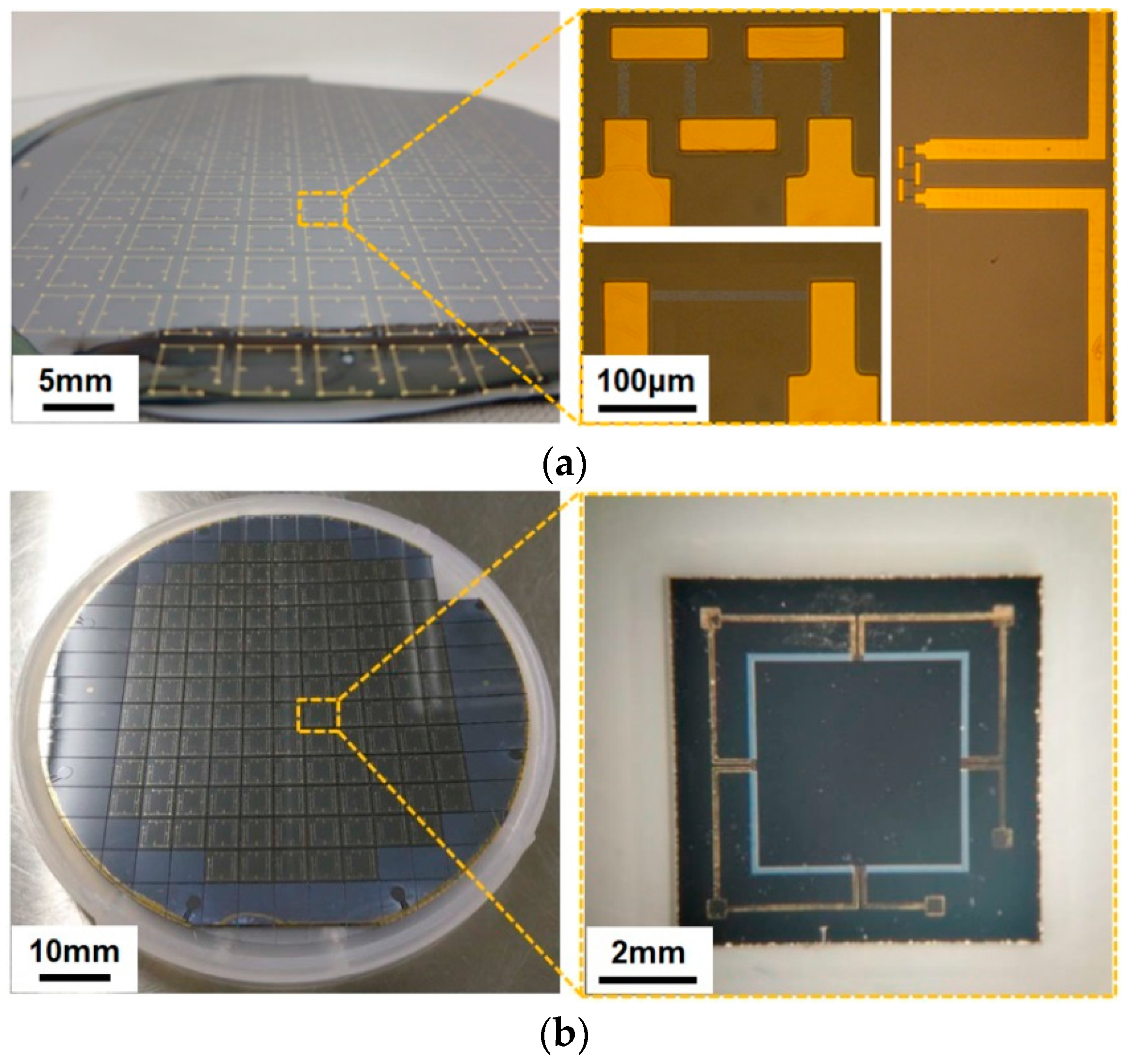
Figure 6.
Photographs of the proposed sensor chip: (a) front side of the wafer after metallization and its two different pattern piezoresistors and (b) photographs of the sensor chip after laser cutting.
Figure 6.
Photographs of the proposed sensor chip: (a) front side of the wafer after metallization and its two different pattern piezoresistors and (b) photographs of the sensor chip after laser cutting.

Figure 7.
Schematic diagram of the assembling: (a) interconnecting structure; and (b) assembled sensor.
Figure 7.
Schematic diagram of the assembling: (a) interconnecting structure; and (b) assembled sensor.

Figure 8.
Experimental schematic diagrams for the proposed sensor: (a) test diagram for bridge resistance; (b) test diagram for output voltage at room temperature (25 °C); and (c) test diagram at different temperatures.
Figure 8.
Experimental schematic diagrams for the proposed sensor: (a) test diagram for bridge resistance; (b) test diagram for output voltage at room temperature (25 °C); and (c) test diagram at different temperatures.


Figure 9.
Output voltage of the sensor versus applied pressure.

Figure 10.
Sensor input–output curves at different temperatures.

Figure 11.
Curve of the sensitivity variation at different temperatures under 1 psi.

Figure 12.
Zero output of the sensor at different temperatures.

Figure 13.
Curve of the resistance variation at different temperatures.


Table 1.
Optimized dimensions of the proposed membrane.
| Parameters | L | H | h | a | b | g |
|---|---|---|---|---|---|---|
| Dimension (μm) | 3600 | 30 | 35 | 200 | 60 | 10 |
Table 2.
Test results of the Wheatstone bridge resistance.
| Sample | R1 (kΩ) | R2 (kΩ) | R3 (kΩ) | R4 (kΩ) |
|---|---|---|---|---|
| Device 1 | 5.123 | 4.866 | 5.469 | 4.773 |
| Device 2 | 6.678 | 6.125 | 6.904 | 6.439 |
| Device 3 | 5.562 | 5.245 | 5.417 | 5.183 |
Table 3.
Technical data of the sensor at the room temperature.
| Parameter | Value | Parameter | Value |
|---|---|---|---|
| Input voltage (V) | 5 | Repeatability (%FSS) | 0.17 |
| Resistance (kΩ) | 6.7 | Hysteresis (%FSS) | 0.12 |
| Zero output (mV) | 14.6 | Accuracy (%FSS) | 0.30 |
| Full range output (mV) | 169.1 | TCS (%FSS/°C) | −0.15 |
| Sensitivity (mV/V/psi) | 30.9 | TCO (%FSS/°C) | 1.8 |
| Pressure nonlinearity (% FSS) | 0.21 | TCR (%FSS/°C) | 0.19 |
Table 4.
Comparison in performance with other pressure sensors at room temperature.
| Sensor | Sensitivity (mV/V/psi) | Pressure Nonlinearity (% FSS) | Accuracy (% FSS) | Full Range Pressure (kPa) |
|---|---|---|---|---|
| Proposed sensor | 30.9 | 0.21 | 0.30 | 6.894 |
| Sensor in [38] | 10.1 | 0.19 | 0.24 | 10 |
| Sensor in [39] | 12.1 | 0.05 | 0.68 | 10 |
| Sensor in [23] | 25.4 | 0.36 | - | 5 |
| Sensor in [40] | 32.1 | 0.25 | 0.34 | 5 |
Table 5.
Comparison in accuracy with other pressure sensors at high temperature.
| Sensor | Pressure Nonlinearity (% FSS) | Repeatability (% FSS) | Hysteresis (% FSS) | Accuracy (% FSS) | Temperature (°C) |
|---|---|---|---|---|---|
| Proposed sensor | 0.25 | 0.19 | 0.14 | 0.34 | 150 |
| Sensor in [41,42] | 0.33 | 0.22 | 0.13 | 0.72 | 60 |
| Sensor in [43] | 0.26 | 0.11 | 0.11 | 0.3 | 200 |
| Sensor in [6] | 0.3 | 0.16 | 0.14 | 0.48 | 200 |
© 2018 by the authors. Licensee MDPI, Basel, Switzerland. This article is an open access article distributed under the terms and conditions of the Creative Commons Attribution (CC BY) license (http://creativecommons.org/licenses/by/4.0/).
Share and Cite
MDPI and ACS Style
Li, C.; Cordovilla, F.; Jagdheesh, R.; Ocaña, J.L. Design Optimization and Fabrication of a Novel Structural SOI Piezoresistive Pressure Sensor with High Accuracy. Sensors 2018, 18, 439. https://doi.org/10.3390/s18020439
AMA Style
Li C, Cordovilla F, Jagdheesh R, Ocaña JL. Design Optimization and Fabrication of a Novel Structural SOI Piezoresistive Pressure Sensor with High Accuracy. Sensors. 2018; 18(2):439. https://doi.org/10.3390/s18020439
Chicago/Turabian StyleLi, Chuang, Francisco Cordovilla, R. Jagdheesh, and José L. Ocaña. 2018. "Design Optimization and Fabrication of a Novel Structural SOI Piezoresistive Pressure Sensor with High Accuracy" Sensors 18, no. 2: 439. https://doi.org/10.3390/s18020439
Note that from the first issue of 2016, this journal uses article numbers instead of page numbers. See further details here.