γ-radiation Sensor Using Optical and Electrical Properties of Manganese Phthalocyanine (MnPc) Thick Film

Department Electronics and Computer Engineering, University of Limerick, Plassey Technological Park, Limerick, Co. Limerick, Ireland
*
Author to whom correspondence should be addressed.
Sensors 2002, 2(5), 174-184; https://doi.org/10.3390/s20500174
Submission received: 16 April 2002
/
Accepted: 10 May 2002
/
Published: 12 May 2002
Abstract
:Manganese phthaloyanine polymer thick films were fabricated using screen-printing techniques. The optical parameters were obtained from the analysis of the absorption spectra over a wavelength range of 385-900nm. The d.c. electrical measurements were carried out in a range of 0-30 volts. The effects of γ-radiation on the optical and the electrical properties were investigated for dosimetry applications. The optical energy band gaps of these films showed a decrease in their values with the increase in the radiation dose. The electronic transition has changed from direct allowed for the as-printed films (unexposed to γ-rays) to indirect allowed for the irradiated samples. Both the as-printed and irradiated Ag/MnPc/Ag devices demonstrated a Schottky conduction mechanism. Both the absorbance and the capacitance of the MnPc thick films displayed a highly consistent linear response to γ-ray exposure.
Introduction
Metal-substituted and metal-free phthalocyanine polymers have recently attracted considerable interest due to their high thermal and chemical stability [1, 2, 3, 4, 5, 6, 7, 8, 9]. The most attractive property of the phthalocyanines is their similarity in structure to the two most important biological molecules; chlorophyll and haemoglobin [10]. Phthalocyanines have been widely used as gas sensors, optical logic displays, solar cells and colour filters [12, 13]. The aim of this paper is to report the changes in both the optical and electrical properties of screen-printed MnPc thick films under the influence of γ-irradiation and the suitability of these devices for dosimetry applications.
It is well-known that the exposure of solid materials to γ-rays induces structural defects known as colour centres. The presence of such colour centres in a thick film matrix gives rise to changes in both the optical and electrical properties of the material, which can be utilised to assess the radiation dose absorbed [14, 15, 16, 17, 18, 19].
Results and Discussion
Effects of γ-Rays on the Abosrption Bands in the UV-Visible region
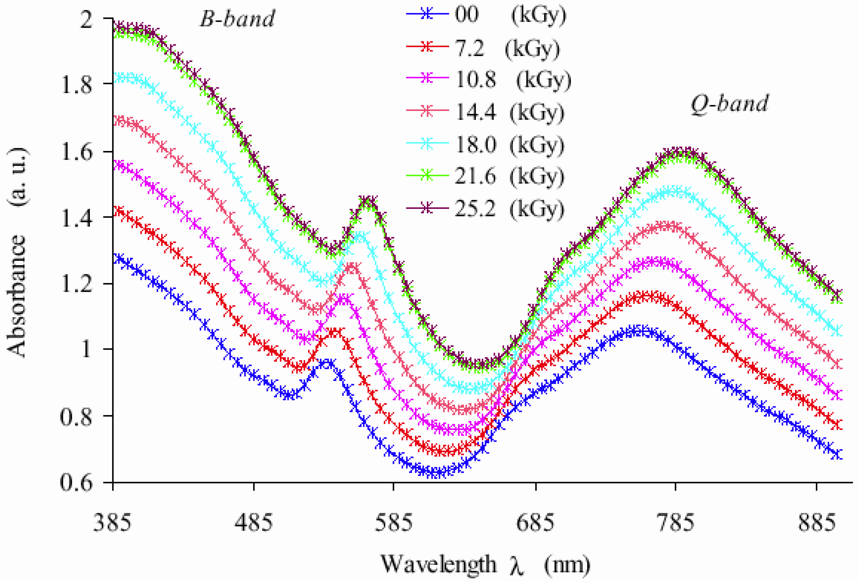
Several absorbance spectra for MnPc thick films exposed to various irradiation doses are illustrated in Figure 1. The lower spectrum is that of the as-printed sample and the upper six spectra are for those exposed to different doses of γ-rays. It was observed that the increase in γ-radiation dose caused an increase in the optical density and also a shift in the spectrum towards higher wavelengths. For instance, when the as-printed MnPc thick films were exposed to a dose of 25 kGy, the following changes were observed:
- 1)
- The centre of the B-band shifted from 385 nm to 396 nm while the absorbance is increased from 2.45 to 3.29.
- 2)
- The Q-band also displayed a similar shift from 756 nm to 786 nm with an increase in absorbance from 1.06 to 1.60.
Further exposure to γ-rays resulted in an even higher absorbance and a greater shift in the UV/Visible spectrum up to a dose of 28 kGy, at which saturation point was reached.
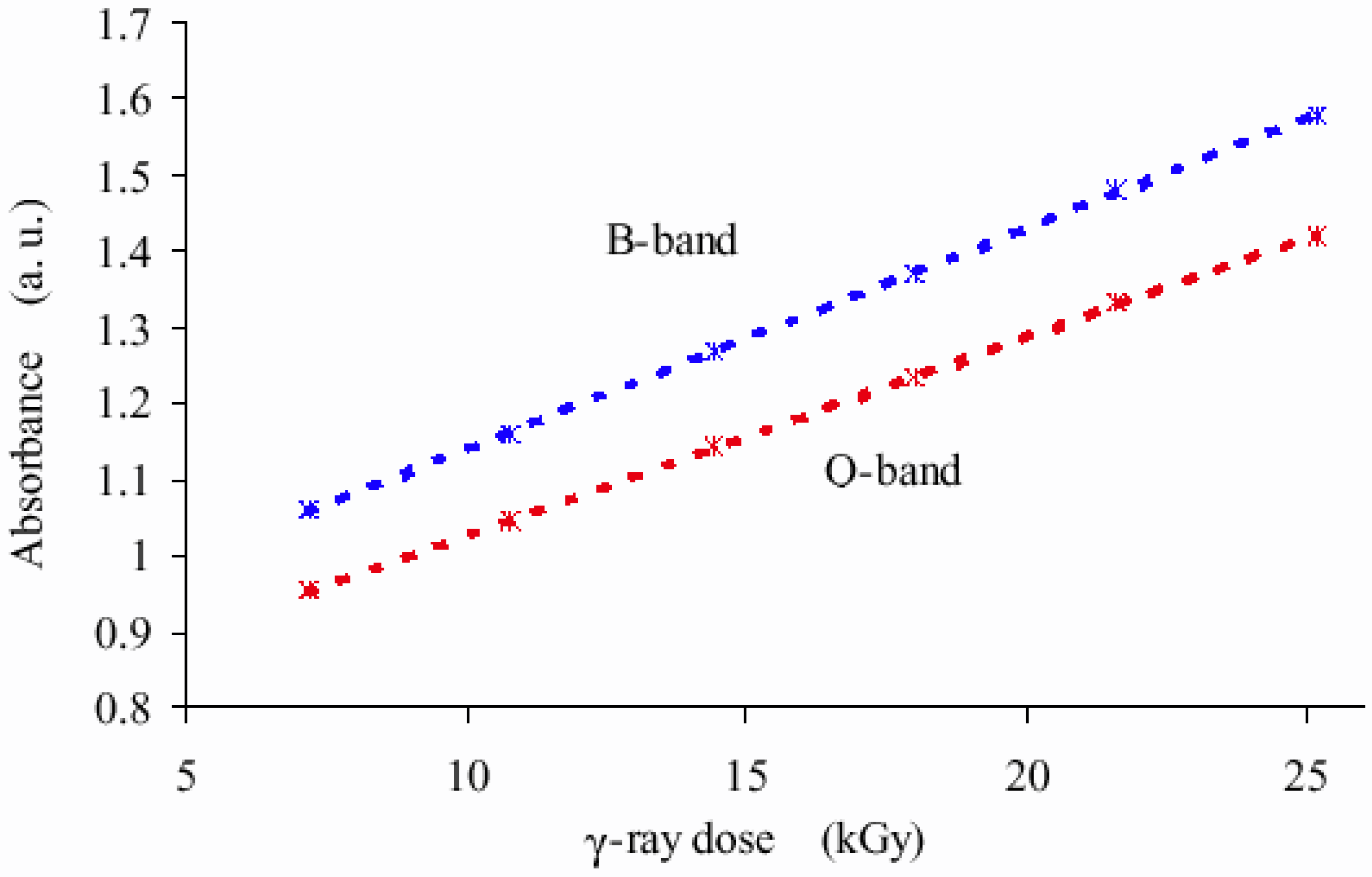
The absorbance of both the B and Q bands increased linearly when exposed to γ-ray doses in the range between 7 kGy - 25 kGy in steps of 3.6 kGy (Figure 2).
Figure 1.
MnPc absorbance spectra display an increase in the absorbance as the γ-ray dose increases. There exists a shift to higher wavelengths as the radiation dose is increased.
Figure 1.
MnPc absorbance spectra display an increase in the absorbance as the γ-ray dose increases. There exists a shift to higher wavelengths as the radiation dose is increased.

Figure 2.
Both B-band and Q-band displayed a linear increase in absorbance in a dose range of 7– 25 kGy.
Figure 2.
Both B-band and Q-band displayed a linear increase in absorbance in a dose range of 7– 25 kGy.

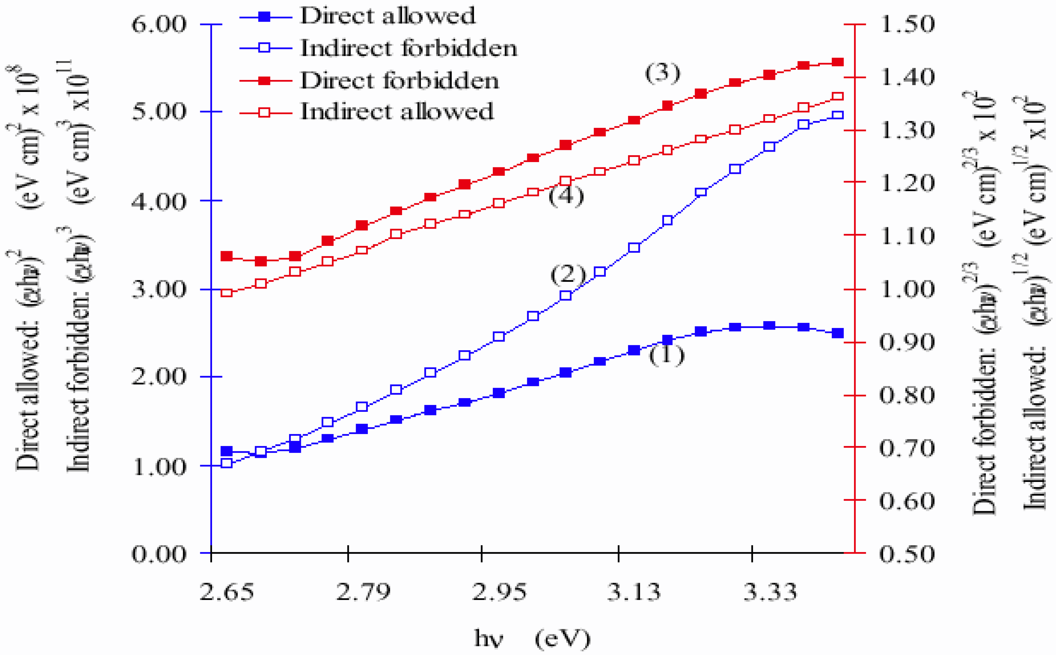
Figure 3.
The transitions of the as-printed MnPc thick films. The best straight line is revealed by curve (1) indicating a direct allowed transition.
Figure 3.
The transitions of the as-printed MnPc thick films. The best straight line is revealed by curve (1) indicating a direct allowed transition.

Effects of γ-rays on the Optical Transitions
Figure 3 represent plots of the four possible optically induced electronic transitions for the manganese-phthalocyanine polymer thick film; a) direct allowed transition, b) indirect allowed transition, c) direct forbidden transition and d) indirect forbidden transition. These transitions were obtained by analysing the absorption edge of the B-band in view of the models proposed by Mott and Davis [20]:
a(ν) hν = B (hν - Eopt)m
Where,α(ν) = 2.303 A/d (A is the absorbance and d is the film thickness), h: Plank’s constant, ν: the frequency of the incident photons, B: constant obtained from the slope of the (αhν) m versus hν (Figure 3 & Figure 4), Eopt: optical energy band gap and m = 1/2, 3/2, 2 or 1/3 for direct allowed, direct forbidden, indirect allowed and indirect forbidden transitions respectively.
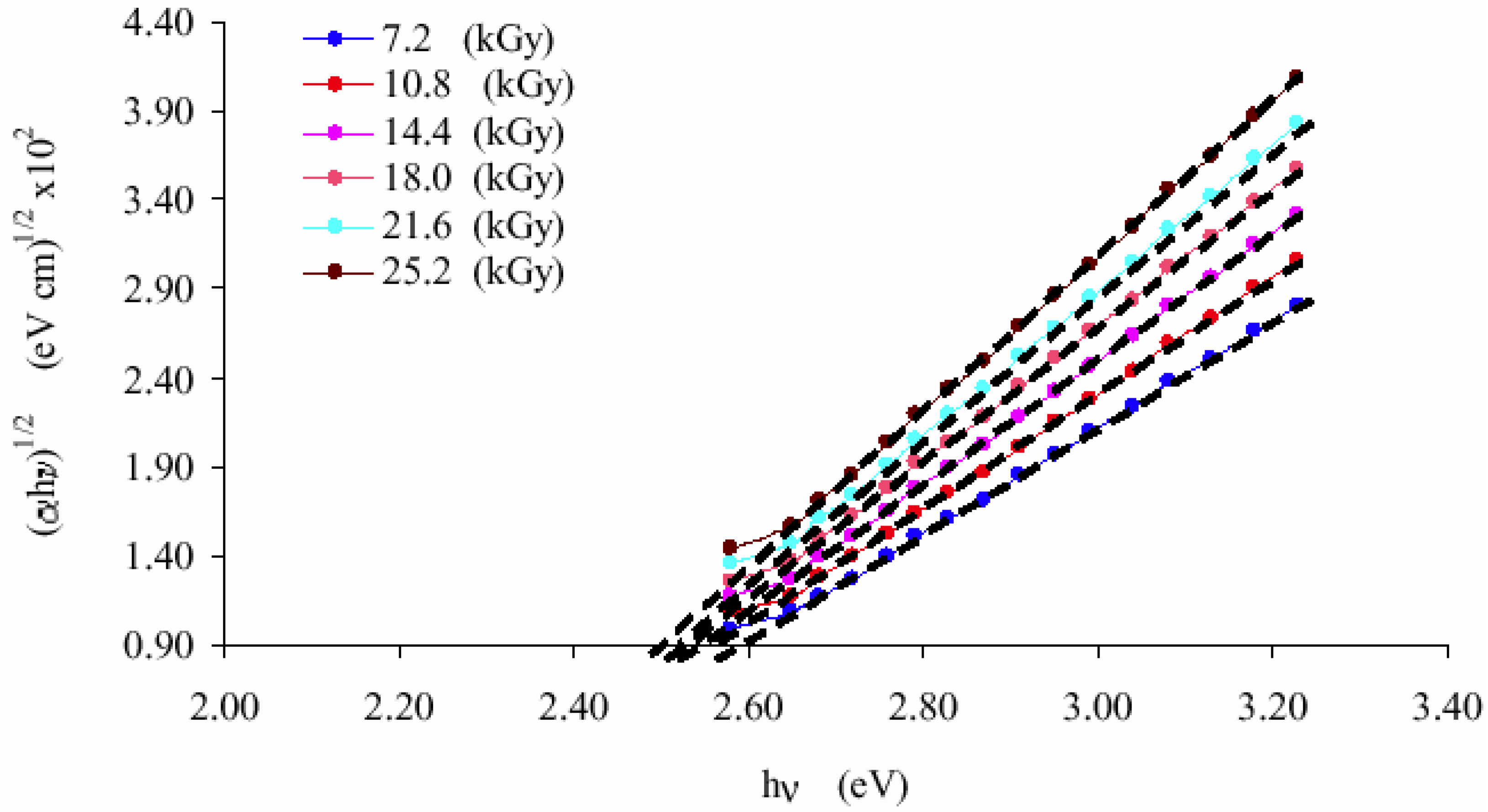
Figure 4.
The effects of γ-rays on the electronic transition of MnPc thick films: The best straight line is revealed by curve (4) indicating a indirect allowed transition.
Figure 4.
The effects of γ-rays on the electronic transition of MnPc thick films: The best straight line is revealed by curve (4) indicating a indirect allowed transition.

In Figure 3, the only satisfactory straight line fit for (αhν)2 as a function of hν is displayed by curve (1). This indicates that the direct allowed transition is the predominant transition for the as-printed MnPc thick films. A similar result has been reported for thin film structures by Rajeh and Menon [4]. However, the indirect electronic transition has been established for the irradiated samples as shown by curve (4) of Figure 4. The change in type of the electronic transitions may be attributed to the increase in the density of traps caused by the exposure to γ-rays, which in turn, increased the disorder. Such increase in structural disorder is indicated by the increase in the width of the tail of the localised states (Ee) from 0.50 eV for the as-printed thick film to 0.55, 0.62, 0.73, 0.78, 0.88 and 0.98 eV when exposed to doses of 7.2, 10.8, 14.4, 18.0, 21.6 and 25.2 kGy respectively.
Effects of γ-rays on the Absorption Edge
The energy values of the optical band gap for MnPc thick films were calculated by assuming the direct allowed transition for the as-printed thick films (m = ½) and indirect allowed transition for the irradiated samples (m=2). Therefore, equation (1) was modified to the forms below:
a(ν) · hν = B · (hν- Eopt)1/2
a(ν) · hν = B · (hν- Eopt)2
The energy value of the absorption edge for the as-printed MnPc thick films was ~ 2.59 eV, which is much lower than the values of 3.14-3.25 eV reported for thin films by Rjesh and Menon [4]. The large difference in energy was attributed to the effect of film thickness on the optical band gap by Ismail etal [21], when investigating various compositions of SiO/Nb2O5 and Nb2O5. They observed that the energy of the optical band gap decreased as the film thickness was increased.
Figure 5 shows plots of (αhν) 2 versus hν for as-printed and irradiated films. It is evident from the curves that the values of the optical band gap has decreased from 2.59 eV for as-printed MnPc to 2.49 eV for films exposed to γ-ray dose of 25.2 kGy. This was attributed to the increase in the disorder caused by the presence of structural defects, which is known to increase the width of the localised states, thus reduce the value of the optical gap [3, 20, 21].
Figure 5.
The extrapolations of straight lines for which (αhν)1/2 = 0.0 display the radiation induced decrease in the optical band gap.
Figure 5.
The extrapolations of straight lines for which (αhν)1/2 = 0.0 display the radiation induced decrease in the optical band gap.

Effects of γ-Rays on the Conduction Mechanism of MnPc Thick Films
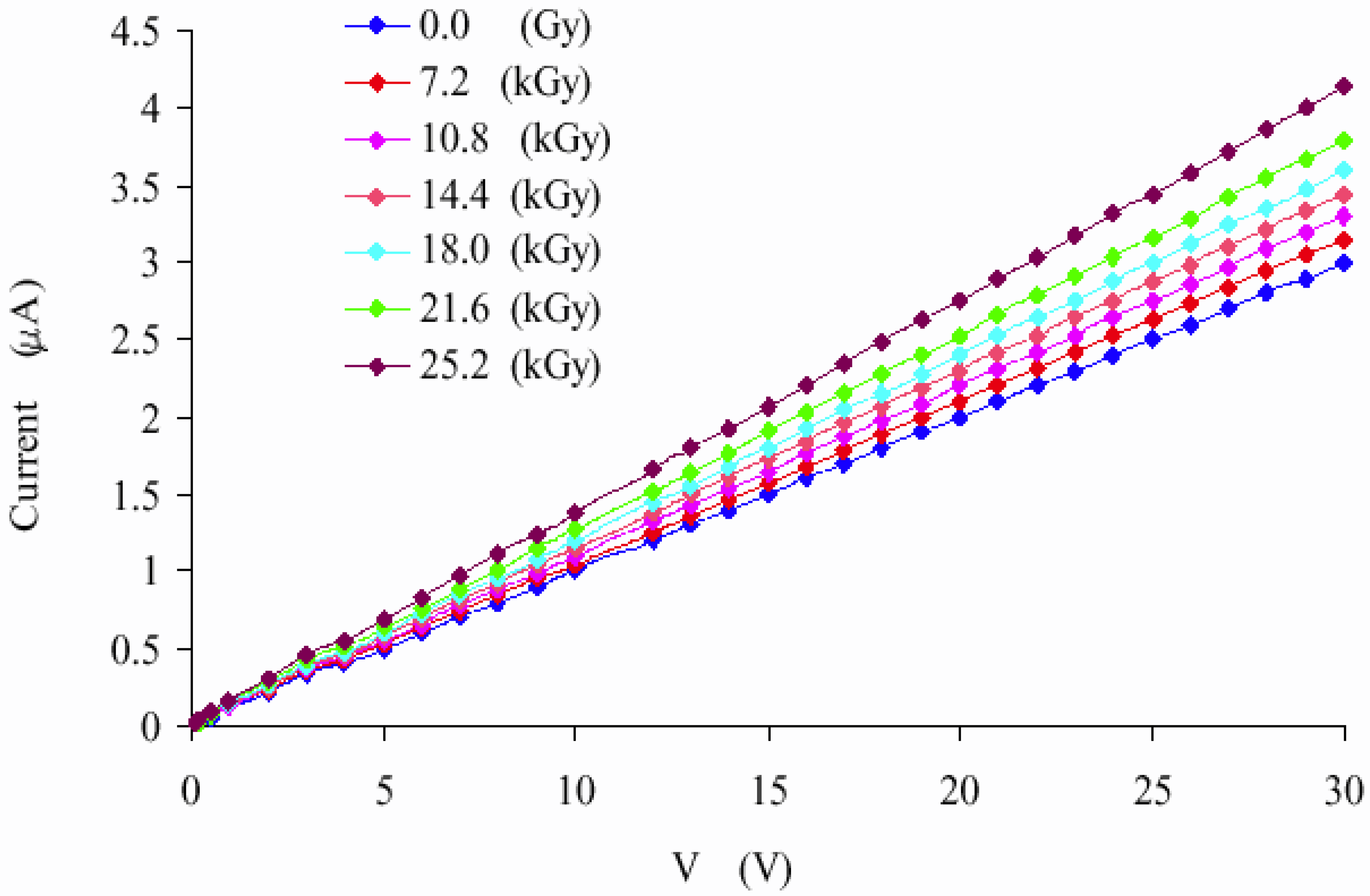
The current-voltage (I-V) characteristics are shown in Figure 6 for MnPc thick film exposed to γ-ray doses ranging from 7 to 25 kGy. There is only one distinct region throughout a voltage range of 0-30 volts for each characteristic curve: at both low and high voltages the slope of I versus V plot was much less than unity indicating the absence of the power-law dependence and the presence of the electrode to bulk-limited effect in the Ag/MnPc contact.
Figure 6.
The I-V characteristics curves display a linear relationship indicting bulk-limited conduction mechanism for the as-printed and irradiated thick films.
Figure 6.
The I-V characteristics curves display a linear relationship indicting bulk-limited conduction mechanism for the as-printed and irradiated thick films.

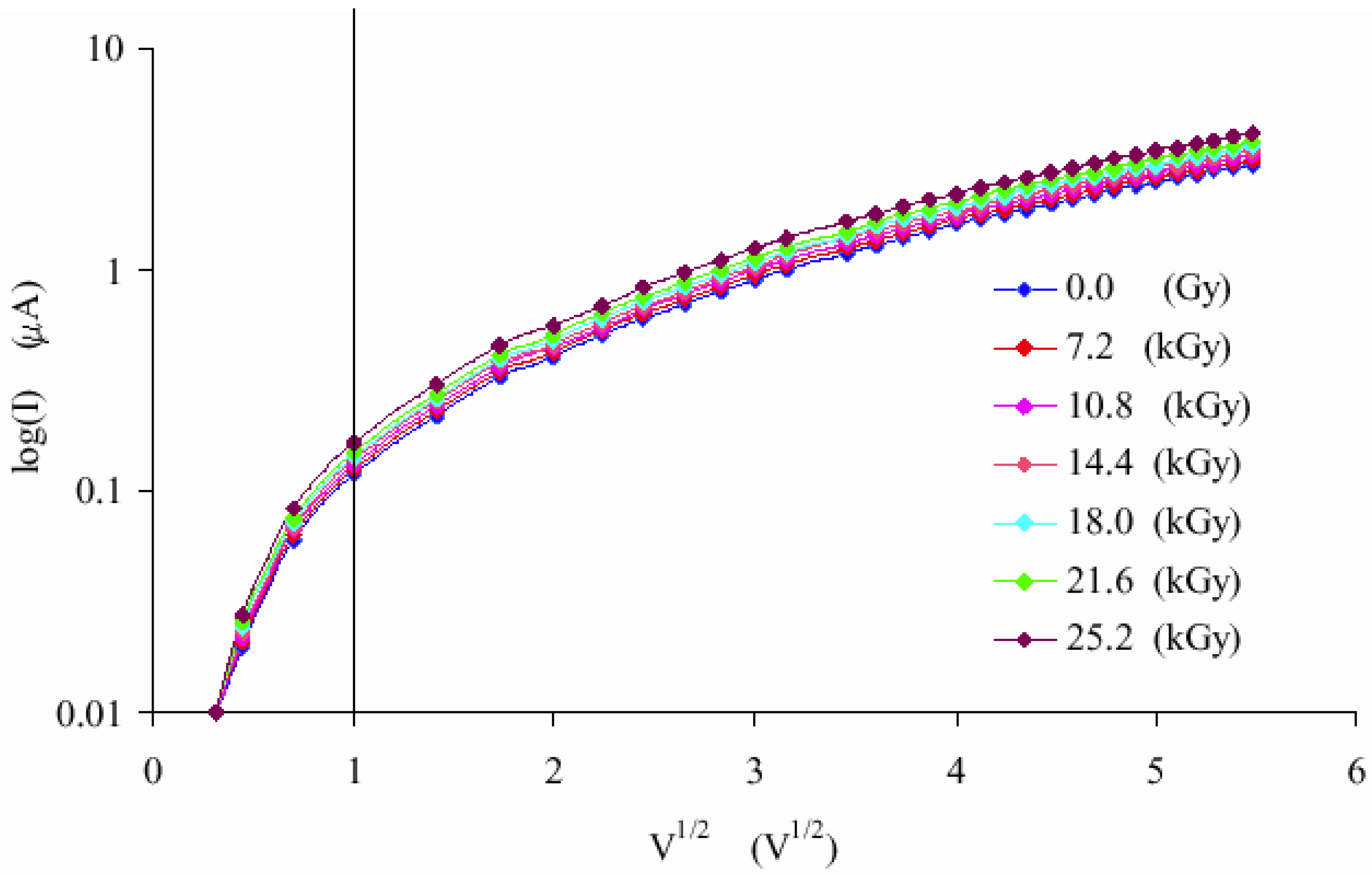
Further analysis is provided by Figure 7, where plots of log(I) versus V1/2 characteristics are displayed. There are two distinct regions for each curve: at voltages lower than 1 volt the current is thickness-independent and rises sharply displaying the electrode-limited region. However, at voltages higher than 1 volt the electron transport is bulk-limited and the effect of MnPc thickness is manifested by the insignificant increase in the current. The bulk-limited conduction mechanism is governed by the following equation:
![Sensors 02 00174 i001]() where, Ic: the circulating current, E: the applied electric field, k: Bolzmann’s constant, T: the absolute temperature (K), β: the high field-lowering coefficient.
where, Ic: the circulating current, E: the applied electric field, k: Bolzmann’s constant, T: the absolute temperature (K), β: the high field-lowering coefficient.

It is also experimentally possible to distinguish between both types of the bulk-limited conduction mechanism: Poole-Frenkel and Richardson-Schottky conductions using the relative permittivity values. The permittivity values listed in Table 1 for the MnPc films, were obtained from both direct measurement using an impedance analyser (HP 4277A LCZ-meter) and estimated by using the high-field lowering coefficients (β) as follows:
![Sensors 02 00174 i002]() where,∈o: Free space permittivity, ∈r: Material’s relative permittivity, e: Electronic charge in coulombs and m = 1 for Poole-Frenkel or m = 4 for the Schottky conduction mechanism [20].
where,∈o: Free space permittivity, ∈r: Material’s relative permittivity, e: Electronic charge in coulombs and m = 1 for Poole-Frenkel or m = 4 for the Schottky conduction mechanism [20].

Figure 7.
log(I) versus V1/4 for MnPc thick film: all films show electrode-limited at low voltages and bulk-limited at high voltages.
Figure 7.
log(I) versus V1/4 for MnPc thick film: all films show electrode-limited at low voltages and bulk-limited at high voltages.

The relative permittivity values listed in Table 1, namely, columns (1) and (3) are within the range of (2.4-5.1) as reported by several workers for phthalocyanine thin film materials [13, 22, 23, 24, 25]. Both columns are highly consistent indicating the predominance of Schottky conduction mechanism for the Ag/MnPc interface.

Table 1.
Comparison of the measured and calculated permittivity values to reveal the type of condition mechanism.
| γ-Ray Exposure Dose (kGy) | High-Field Lowering Coefficient β×10-5 (eV V-1/2cm1/2) | Relative Permittivity | ||
|---|---|---|---|---|
| Measured LCZ-meter (1) | Poole-Frenkel Effect (2) | Schottky Emission (3) | ||
| 0.0 | 70 | 2.5 | 12.36 | 2.6 |
| 7.2 | 75 | 2.8 | 11.57 | 3.11 |
| 10.8 | 78 | 3.2 | 10.83 | 3.3 |
| 14.4 | 84 | 3.6 | 10.23 | 3.5 |
| 18.0 | 89 | 3.9 | 9.49 | 3.8 |
| 21.6 | 95 | 4.2 | 9.13 | 4.05 |
| 25.2 | 101 | 4.6 | 8.52 | 4.44 |
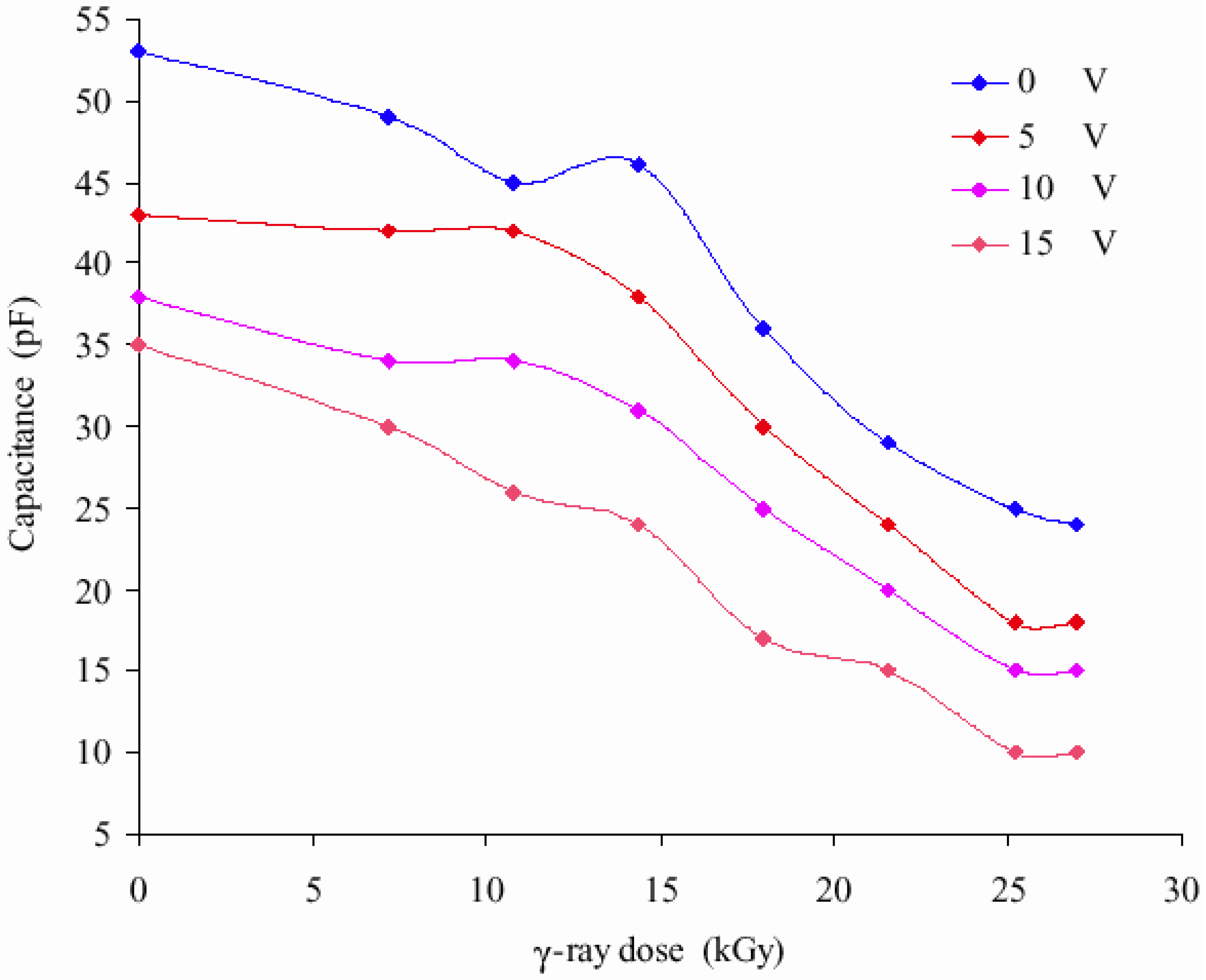
Effect of γ-Rays on the Capacitance of MnPc Thick Films
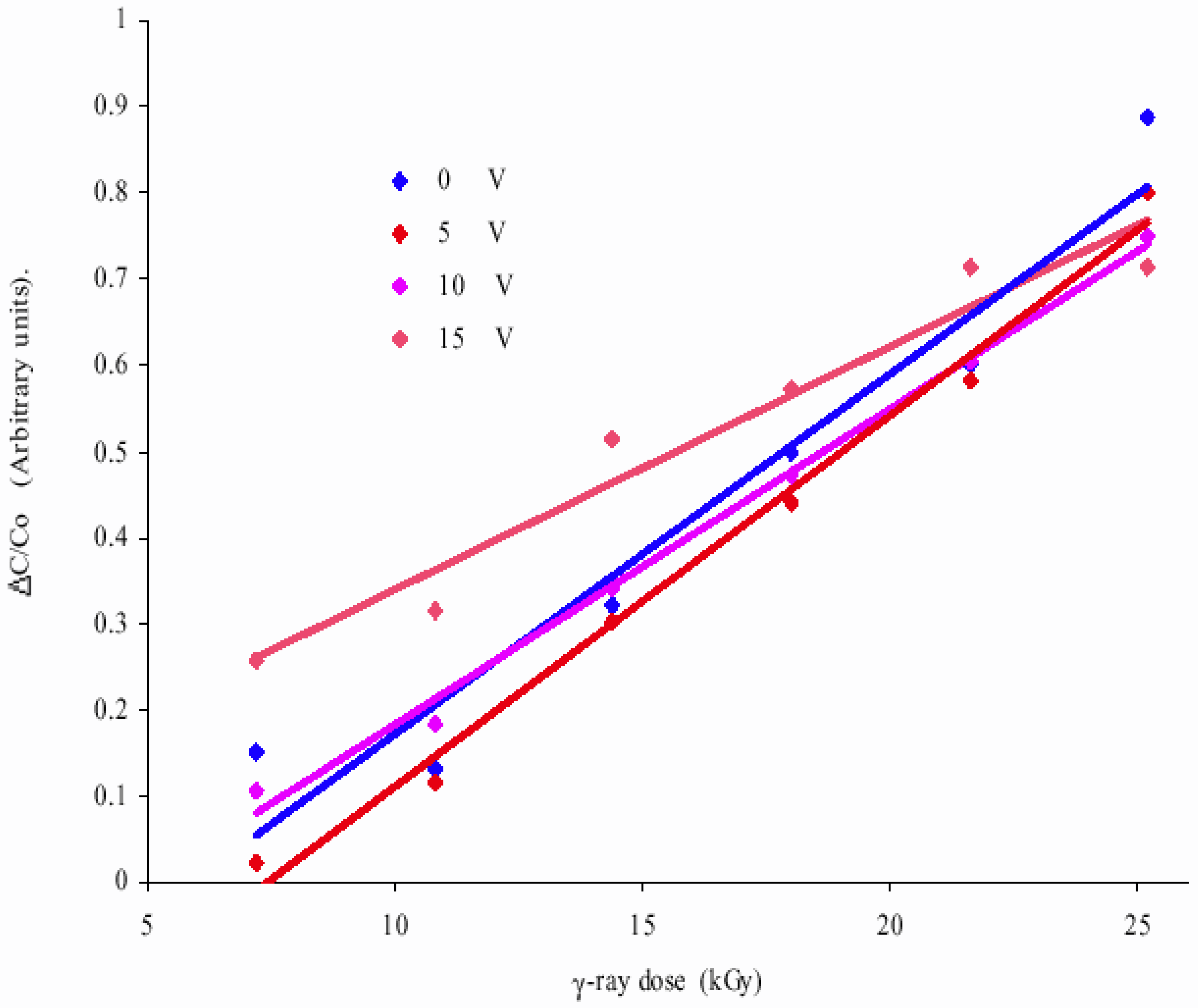
The effects of γ-radiation on the capacitance (C) of Ag/MnPc/Ag devices under different voltages is presented in Figure 8. The samples showed no significant changes when they were exposed to γ-ray dose below 7.2 kGy. However, when the dose was increased, the capacitances of the MnPc samples were decreased. Further exposure to γ-radiation led to a continuous decrease in capacitance values until reaching saturation dose beyond 25.2 kGy. In Figure 9, linear relationships between the ΔC/Co and γ-ray dose (D) are shown for different working voltages where ΔC/Co = (Co − C)/C. In addition, continuous linear changes in the capacitance of the Ag/MnPc/Ag were recorded for γ-ray dose exposure ranging within 7.2-25 kGy suggesting the suitability of using screen-printed MnPc thick films for high dose dosimeters.
Figure 8.
The decrease in the capacitance as with the increase in γ-ray dose.

The MnPc polymer thick films are comparable in properties and dosimetry range to the thin dyed-plastic dosimeter investigated by Abdel-Rehim etal [26]. The advantage of MnPc thick film over the thin dyed-plastic is that the former is a heat stable upto temperature of 200 °C (the melting point of the binding polymer) while the latter is unstable at a temperature of 60 °C or higher.
Figure 9.
Linear relationships between ΔC/Co and γ-ray dose at different voltages.

Experimental
Capacitive devices were fabricated using polymer thick-film technology. The dielectric layer consisted of a polymer paste, which was made from 90% MnPc and 10% Polyvinyl Butyral (PVB) by weight, with Butyl Carbitol (Diethylenglycol-monobutylether) being the main solvent. Conductive DuPont 4929 silver was used as contacts on both sides of the dielectric layers of MnPc thick film. All layers were printed using a DEK 1202 automatic screen printer with a 325-mesh stainless steel screen at an angle of 45° to the frame. Thicker films having a thickness of 60 μm were fabricated for the Ag/NiPc/Ag devices by successively printing layers of MnPc paste on top of each other. Each printed layer was dried in a curing oven. This thickness was verified by following a standard procedure using an optical microscope [27].
Several Ag/MnPc/Ag devices were fabricated in an MIM (Metal-Insulator-Metal) structure with an active area of 1.0 cm x 1.0 cm. Simple ohmic circuit was constructed for measurements of I-V characteristics. An impedance analyser (HP 4277A LCZ-meter) was used to measure the capacitance of both as-deposited and irradiated devices under an excitation frequency of 500 Hz.
In the case of optical measurements a thickness of 15μm was sufficient. The UV/Visible spectra were recorded for the as-printed and irradiated samples at room temperature using a Varian DMS-100S UV-visible spectrometer. The samples were independently exposed to doses of γ-radiation (7.2-25.2 kGy) from a 137Cs source at a dose rate of 6.0 Gy/min.
Conclusion
The optical and electrical properties of screen-printed Manganese-Phthalocyanine thick films were investigated before and after exposure to γ-radiation, to explore the possibility of their use in dosimetry applications. A satisfactory straight line fit was shown by (αhν) 2 as a function of hν for the as-printed MnPc thick films, which indicated the predominance of a direct allowed transition within the band gap. The (αhν) 1/2 versus hν revealed the best straight line for the irradiated samples indicating the predominance of the indirect allowed transition. In addition, continuous linear changes in both the optical absorbance and the capacitance of the Ag/MnPc/Ag were recorded for γ-ray dose exposure ranging within 7.2-25 kGy suggesting the suitability of sreen-printed MnPc thick films for dosimetry applications.
References and Notes
- Arshak, A.; Zleetni, S.M.; Arshak, K.I.; Harris, J. Proc. IEEE-NANO 2001, Maui, Hawaii, USA, 28-30 October, 2001; pp. 238–243.
- Arshak, A.; Zleetni, S.M.; Arshak, K.I.; Harris, J. Proc. IEEE-23rd International Conference on Microelectronics, Nis, Yugoslavia, 12-15 May 2002.
- Arshak, A.; Zleetni, S.M.; Arshak, K.I.; Harris, J. Proc. IEEE-23rd International Conference on Microelectronics, Nis, Yugoslavia, 12-15 May 2002.
- Rajesh, K.R.; Menon, C.S. Materials Letters 2001, 51, 266–269.
- Gravano, S.; Hassan, A.K.; Gould, R.D. Int. J. Electronics 1991, 70, 477–484.
- Amer, N.; Gould, R.D.; Saleh, A.M. Vacuum 1998, 50, 53–56.
- Guttman, F.; Lyons, L.E. Organic Semiconductor; A.Kriegers: Malabar, 1981. [Google Scholar]
- Leznoff, C.C.; Lever, A.B.P. Phthalocyanines: Properties and Applications; 3; VCH: New York, 1993. [Google Scholar]
- Ambily, S.; Menon, C.S. Thin Solid Films 1999, 247, 284–288.
- Nalwa, H.S.; Kakuta, A. Thin Solid Films 1995, 254, 218–223.
- Hassan, A.K.; Gould, R.D. Int. J. Electronics 1990, 69, 11–17. [CrossRef]
- Hoshi, H.; Dann, H.; Marayama, Y. J. Appl. Phys. 1990, 67, 1845–1849. [CrossRef]
- Gould, R.D. 1985, 125, 63–69.
- Christman, J.R. Fundamentals of Solid State Physics; John Wiley & Sons: New York, 1988. [Google Scholar]
- Knoll, G. Radiation Detection and Measurement; 2nd ed; John Wiley & Sons: New York, 1989. [Google Scholar]
- Holmes-Siedle, A.; Adams, L. Handbook of Radiation Effects; Oxford University Press: Oxford, U.K., 1994. [Google Scholar]
- Dearnaley, G.; Northrop, D.C. Semiconductor Counters for Nuclear Radiations; E. & F. N. Spon Ltd.: London, U.K., 1966. [Google Scholar]
- Evans, R.D. The Atomic Nucleus; Robert E. Krieger Publications. Co.: Malabar, Florida, USA, 1955. [Google Scholar]
- Krane, S.K. Introductory Nuclear Physics; John Wiley & sons: New York, 1988. [Google Scholar]
- Mott, N F.; Davis, E.A. Electronic Process in Non-crystalline Materials; 2nd ed; Clarendon Press: Oxford, UK, 1979. [Google Scholar]
- Al-Ismail, J.S.A.Y.; Arshak, K.; Hogarth, C.A. Phys. Stat. Sol. (A) 1985, 89, 363–374.
- Sussman, A. J. Appl. Phys. 1967, 38, 2738–2748.
- Hamann, C. Phys. Status Solidi 1968, 26, 311–318.
- Gould, R.D. J. Phys. D: Appl. Phys. 1986, 9, 1785–1790.
- Delcote, G.M.; Fillard, J.P.; Marco, F.J. Solid State Commun. 1964, 2, 373–376.
- Abdel-Rehim, F.; Ebraheem, S.; Wei-Zhen, Ba.; Mclaughlin, W.L. Appl. Radiat. Isot. 1992, 43, 1503–1510.
- Prudenziati, M. (Ed.) Handbook of Sensors and Actuators: Thick Film Sensors; Elsevier Science B. V.: Amsterdam, The Netherlands, 1994.
- Sample Availability: Available from the authors.
© 2002 by MDPI (http://www.mdpi.net). Reproduction is permitted for noncommercial purposes.
Share and Cite
MDPI and ACS Style
Arshak, A.; Zleetni, S.; Arshak, K. γ-radiation Sensor Using Optical and Electrical Properties of Manganese Phthalocyanine (MnPc) Thick Film. Sensors 2002, 2, 174-184. https://doi.org/10.3390/s20500174
AMA Style
Arshak A, Zleetni S, Arshak K. γ-radiation Sensor Using Optical and Electrical Properties of Manganese Phthalocyanine (MnPc) Thick Film. Sensors. 2002; 2(5):174-184. https://doi.org/10.3390/s20500174
Chicago/Turabian StyleArshak, A., S. Zleetni, and K. Arshak. 2002. "γ-radiation Sensor Using Optical and Electrical Properties of Manganese Phthalocyanine (MnPc) Thick Film" Sensors 2, no. 5: 174-184. https://doi.org/10.3390/s20500174