Fabrication of Thin-Film LAPS with Amorphous Silicon
by
Tatsuo Yoshinobu
1,*, 
Michael J. Schöning
2,3,
Friedhelm Finger
4,
Werner Moritz
5 and
Hiroshi Iwasaki
1 1
ISIR, Osaka University, 8-1 Mihogaoka, Ibaraki, Osaka 567-0047, Japan
2
University of Applied Sciences, Aachen (Division Jülich), Laboratory for Chemical Sensors and Biosensors, Ginsterweg 1, D-52428, Jülich, Germany
3
ISG-2, Research Centre Jülich, 52425 Jülich, Germany
4
IPV, Research Centre Jülich, 52425 Jülich, Germany
5
Humboldt University Berlin, Brook-Taylor-Str. 2, 12489 Berlin, Germany
*
Author to whom correspondence should be addressed.
Sensors 2004, 4(10), 163-169; https://doi.org/10.3390/s41000163
Submission received: 9 August 2004
/
Accepted: 27 August 2004
/
Published: 30 October 2004
Abstract
:To improve the spatial resolution of the light-addressable potentiometric sensor (LAPS), it is necessary to reduce the thickness of the semiconductor layer, which, however, causes a problem of the mechanical strength of the sensor plate. In this study, a thin-film LAPS was fabricated with amorphous silicon (a-Si) deposited on a transparent glass substrate. The current-voltage characteristics and pH sensitivity of the fabricated a-Si LAPS were investigated.
Introduction
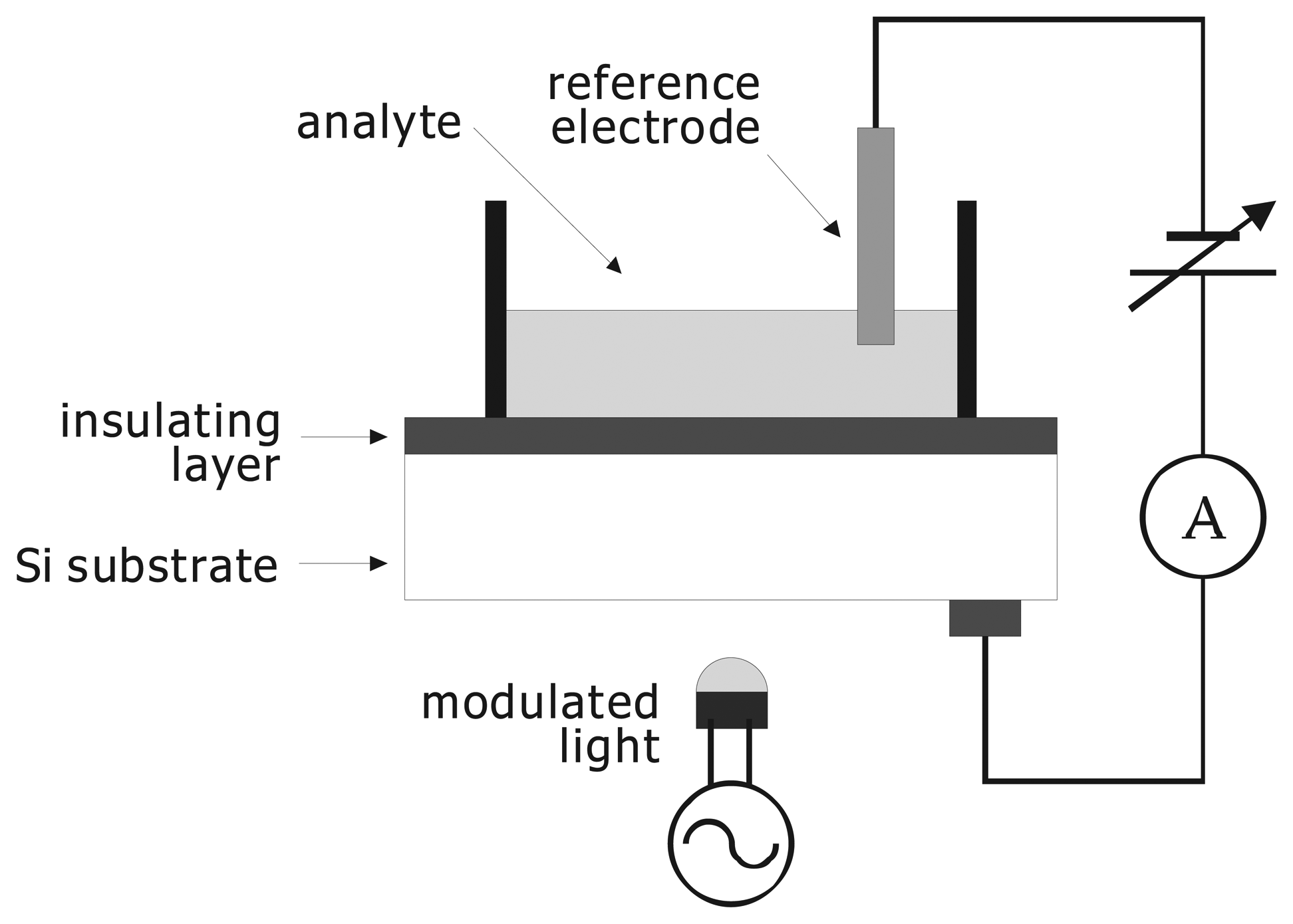
The light-addressable potentiometric sensor (LAPS) [1,2] is a semiconductor-based chemical sensor with an electrolyte-insulator-semiconductor (EIS) structure as shown in Fig. 1. The principle of the LAPS is similar to that of the EIS capacitance sensor, in which the capacitance of the EIS system is measured to determine the ion concentration of the solution. In the case of the EIS capacitance sensor, however, the obtained value of the ion concentration is an average over the whole sensing surface in contact with the solution [3,4]. In contrast, the LAPS measurement is spatially resolved. The measured area on the sensing surface is defined by illumination, which generates the ac photocurrent to be measured.
Because of this “light-addressability”, LAPS can be used as a basis of an integrated multisensor [5], in which more than one measuring point on the sensing surface is individually accessed by the light. The LAPS is also a basis of the chemical imaging [6,7], in which a focused laser beam scans the sensing area to visualize the two-dimensional distribution of the ion concentration.
The spatial resolution of the LAPS is an important factor for both the multisensor application and for the chemical imaging application. It limits the density of measuring points on the multisensor surface and the smallest size of structures that can be visualized by the chemical imaging sensor. It has been demonstrated both experimentally and theoretically [8-10] that the spatial resolution is determined by the beam size and the lateral diffusion of photocarriers in the semiconductor substrate. With appropriate focusing optics, the beam size can be reduced down to the scale of 1 μm or the wavelength of the light. The lateral diffusion is determined by the thickness of the semiconductor layer as well as by the material parameters such as the diffusion length of minority carries and the absorption coefficient of the light.
Within the last years, several attempts have been made to improve the spatial resolution of the LAPS and the chemical imaging sensor by thinning the Si substrate [9], using a silicon-on-insulator (SOI) substrate [11] and using a GaAs substrate [12].
In this study, a thin-film LAPS was fabricated with amorphous silicon (a-Si) deposited on a transparent glass substrate. Instead of thinning the sensor plate, the thickness of the semiconductor layer can be defined by the deposition rate and deposition time from the gaseous phase. Recently, a-Si has been successfully applied to other chemical sensors, which are based on field-effect structures [13-17]. In the case of an a-Si ion-sensitive field-effect transistor (a-ISFET), pH sensitivities of 48 mV/pH [13] and 46 mV/pH [14] are reported. With a K+ ion-sensitive thin-film transistor (ISTFT) with a valinomycin-doped PVC membrane, a K+ sensitivity of 63 mV/pK is reported. Because of the feasibility of large-area thin films and the availability of the mature technologies, a-Si is expected to be an ideal material for a high-resolution LAPS.
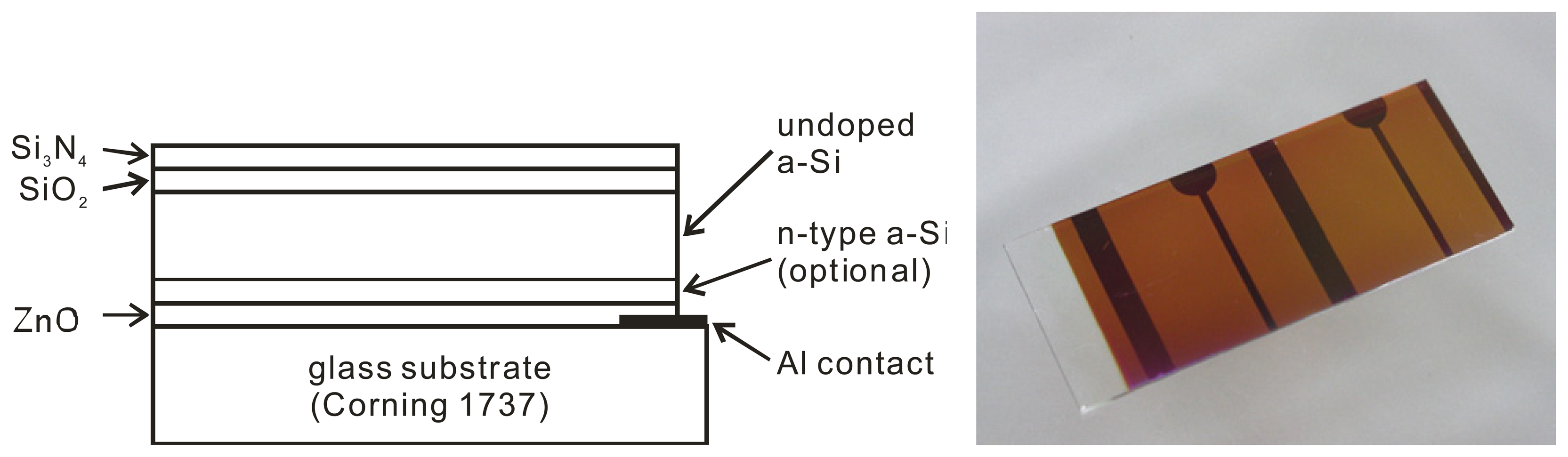
Preparation of a-Si LAPS
Figure 2 shows the layer structure of the fabricated a-Si LAPS device. Two different structures of the a-Si LAPS have been prepared:
- glass/ZnO/n-type a-Si/undoped a-Si/SiO2/Si3N4 (type I),
- glass/ZnO/undoped a-Si/SiO2/Si3N4 (type II).
For each structure (type I, type II), three samples with different thickness of the undoped a-Si layer (0.4, 0.7 and 1.2 μm) have been prepared. The a-Si thin films have been fabricated by the conventional glow discharge method on Corning 1737 glass substrates with 500 nm of Al grids and 700 nm of transparent ZnO layer as the backside contact. The deposition parameters for the n-type a-Si layer (optional) and the undoped a-Si layer are summarized in Table 1. Phosphine (PH3) was used for the n-type doping.
After the deposition of the a-Si layer(s), the insulating layers of SiO2 and Si3N4 were prepared by the plasma-enhanced chemical vapor deposition (PECVD) method. The thickness of the SiO2 and Si3N4 layer has been 30 nm and 50 nm, respectively. Prior to the measurement, the pH-sensitive surface of Si3N4 was activated by a short dip in dilute HF (1%, for 10 sec.).
Characteristics of a-Si LAPS
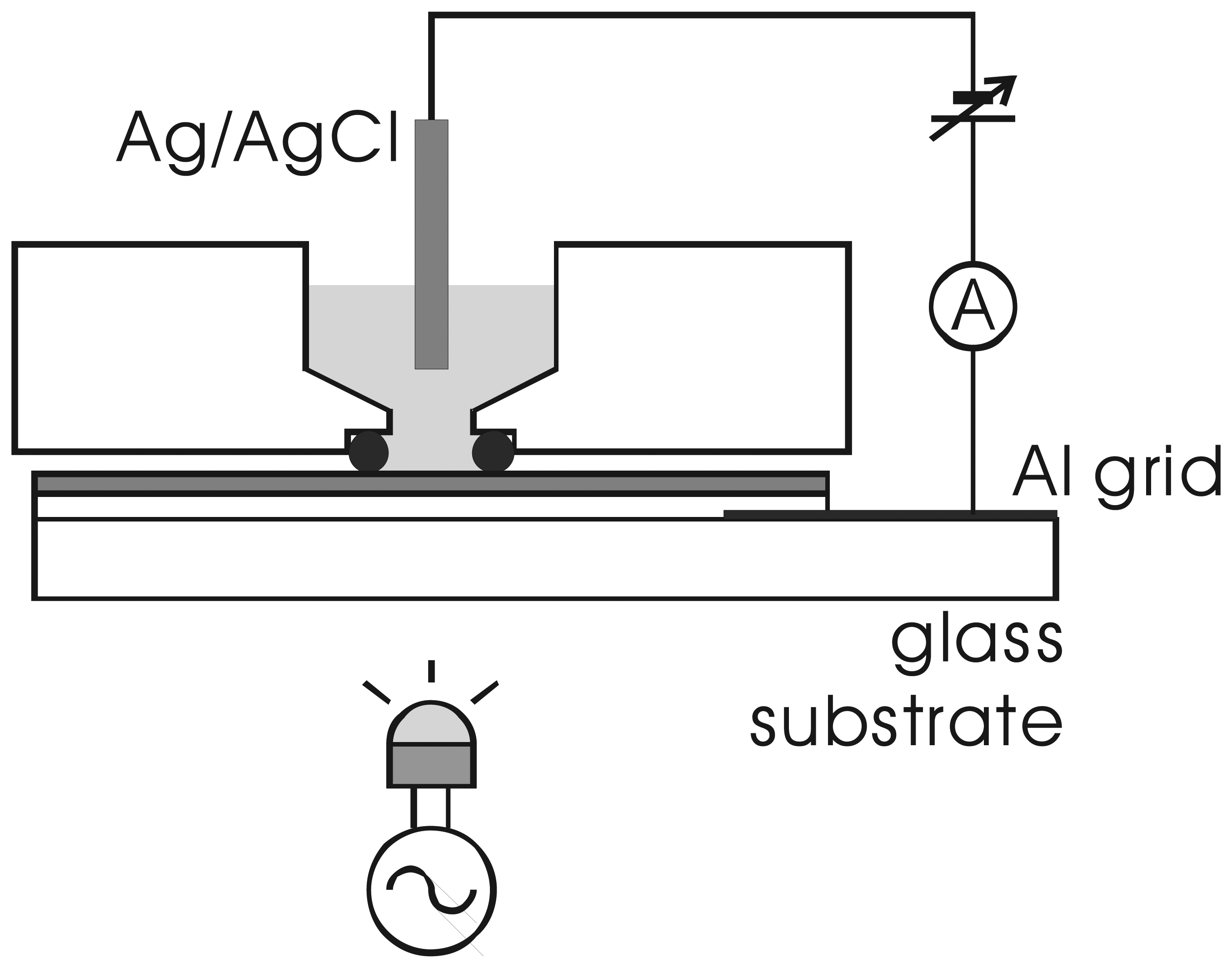
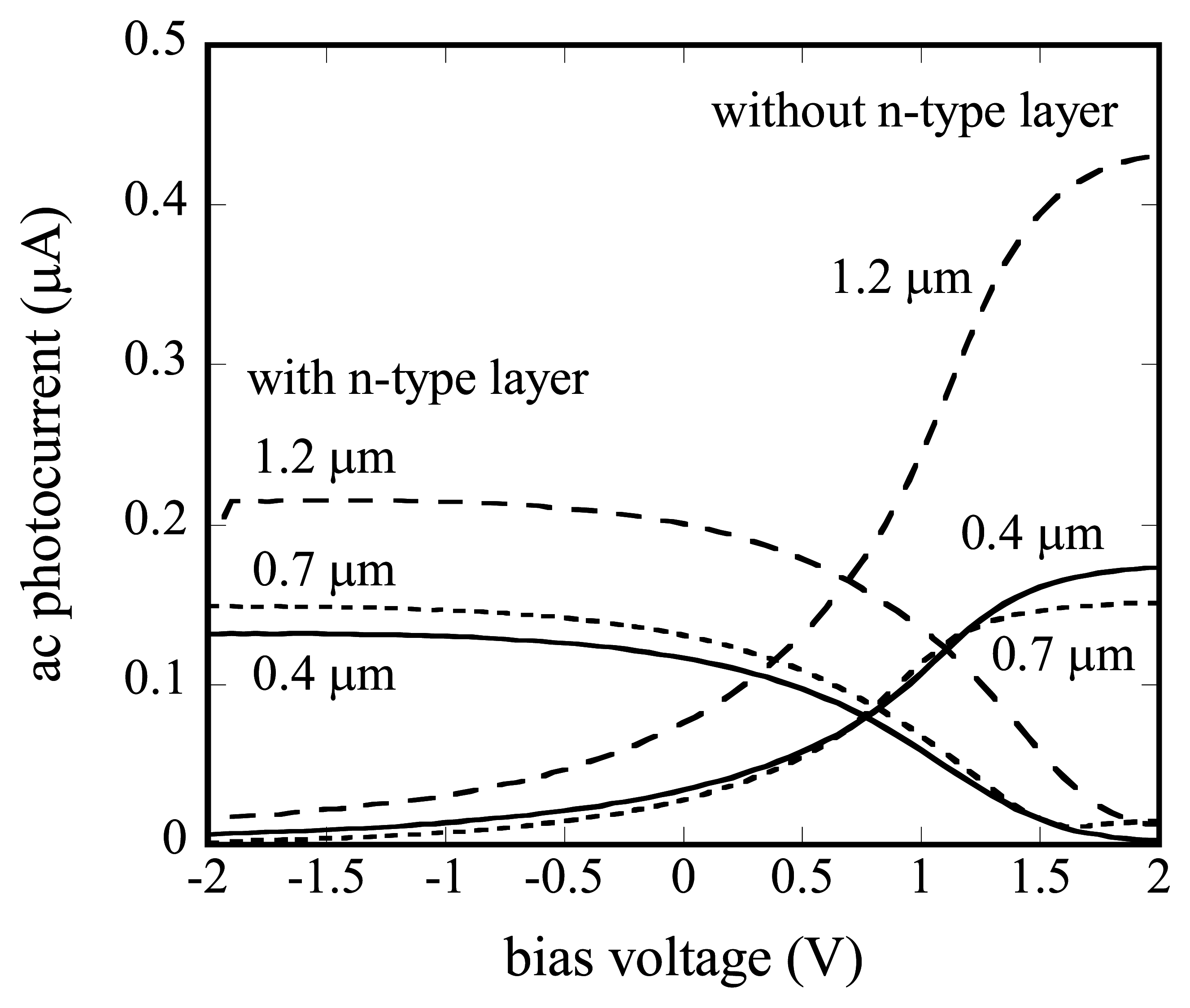
The current-voltage characteristics of the fabricated sensors were measured in a cell shown in Fig. 3. The measured area on the sensor surface was defined by the O-ring with an inner diameter of about 8 mm. Figure 4 shows the current-voltage characteristics of the a-Si LAPS with (type I) and without (type II) the n-type layer for a pH7 buffer solution (Titrisol, Merck). In this experiment, the bias voltage is defined as the voltage applied to the solution with respect to the Al grid on the glass substrate.
For the a-Si LAPS with the n-type layer (type I), the obtained curves are similar to those of a conventional n-type LAPS. In the present case, the photocarriers (electrons and holes) are separated by the electric field in the undoped layer, whereas the separation of photocarriers in a conventional LAPS is limited only inside the depletion layer. For the a-Si LAPS without the n-type layer (type II), the polarity of the curve was opposite.
As for the dependence on the thickness of the semiconductor layer, the photocurrent increases as the undoped a-Si layer becomes thicker. This can be explained as a result of the increased absorption of the light. On the other hand, in the case of a conventional LAPS, which has a relatively thicker substrate, the light is totally absorbed within the semiconductor layer and the generation of photocarriers is no more dependent on the thickness of the substrate. In this case, the photocurrent decreases as the Si substrate becomes thicker, due to recombination of minority carriers in the substrate.
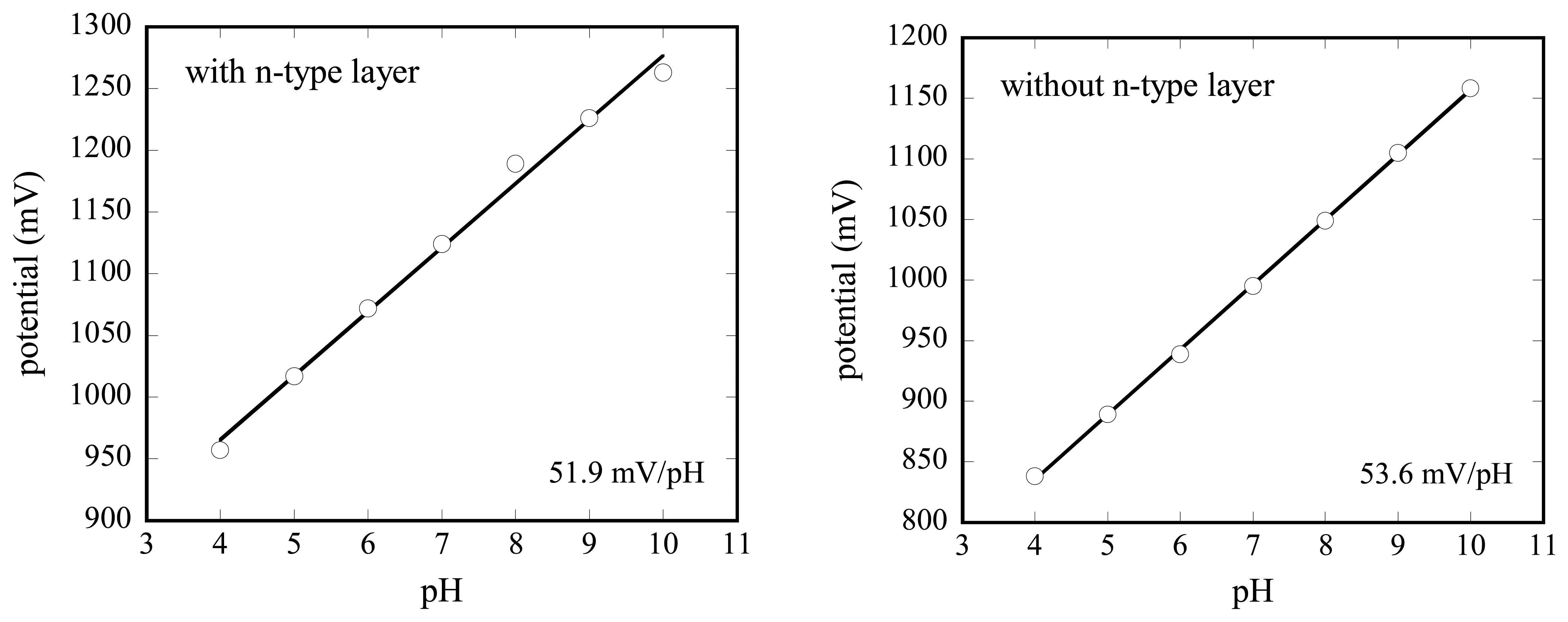
Figure 5 shows the response of the a-Si LAPS with 0.4 μm of undoped a-Si layer to different pH values. In both cases, with (type I) and without (type II) the n-type layer, the current-voltage curve shifts along the voltage axis depending on the pH value from 4 to 10. A linear relationship between the respective pH value and the bias voltage was observed for all sensors, independent of the thickness of the a-Si layer (0.4 μm / 0.7 μm / 1.2 μm).
To calculate the pH sensitivity, the bias voltage corresponding to the inflection point of each curve in Fig. 5 was calculated and plotted versus the pH value in Fig. 6. For the a-Si LAPS with the layer thickness of 0.4 μm, the pH sensitivity is calculated to be about 52 (type I) and 54 mV/pH (type II), respectively. Similar values were obtained also for the a-Si LAPS with the layer thickness of 0.7 μm and 1.2 μm. These sensitivity values correspond very well to those, described in literature for Si3N4 as pH-sensitive material, also deposited by means of the PECVD process [18].
The results indicate the possibility of a-Si as a semiconductor material for thin-film LAPS. In addition to the high spatial resolution, the feasibility of large-area sensors and the low fabrication cost are advantages of a-Si LAPS. It would be necessary, however, to test other aspects of the sensor such as hysteresis and durability, to check the spatial resolution by means of a focused laser beam, and to evaluate the usability of the a-Si LAPS in practical applications.
Summary
In this study, a-Si LAPS has been fabricated on a transparent glass substrate. Two different structures: glass/ZnO/n-type a-Si/undoped a-Si/SiO2/Si3N4 (type I) and glass/ZnO/undoped a-Si/ SiO2/Si3N4 (type II) were compared. The former structure of LAPS showed current-voltage characteristics similar to those of LAPS with n-type semiconductor, while the latter showed an opposite polarity. The a-Si LAPS possesses a nearly-Nernstian pH sensitivity, defined by the PECVD Si3N4 layer on top of the sensor structure. In addition to the high spatial resolution of thin-film LAPS, a-Si is also advantageous for its flexibility of application, as it can be easily deposited on a glass substrate; for example, a-Si LAPS may be integrated as a sensing element in μ-TAS or lab-on-a-chip devices [19].
Acknowledgments
This work was partially supported by the Ministry of Education, Culture, Sports, Science and Technology of Japan (Grant-in-Aid for Scientific Research) and also by the Ministry for Science and Research of Nordrhine-Westfalia, Germany.
References
- Hafeman, D.G.; Wallace, J.P.; McConnell, H.M. Light-addressable potentiometric sensor for biochemical systems. Science 1988, 240, 1182. [Google Scholar]
- Owicki, J.C.; Bousse, L.J.; Hafeman, D.G.; Kirk, G.L.; Olson, J.D.; Garret, W.H.; Wallace, J.P. The light-addressable potentiometric sensor: Principles and biological applications. Annu. Rev. Biophys. Biomol. Struct. 1994, 23, 87. [Google Scholar]
- Poghossian, A.; Thust, M.; Schroth, P.; Steffen, A.; Lüth, H.; Schöning, M.J. Penicillin detection by means of silicon-based field-effect structures. Sensors and Materials 2001, 13, 207. [Google Scholar]
- Poghossian, A.; Yoshinobu, T.; Simonis, A.; Ecken, H.; Lüth, H.; Schöning, M.J. Penicillin detection by means of field-effect based sensors: EnFET, capacitive EIS sensor or LAPS? Sensors and Actuators B 2001, 78, 237. [Google Scholar]
- Shimizu, M.; Kanai, Y.; Uchida, H.; Katsube, T. Integrated biosensor employing a surface photovoltage technique. Sensors and Actuators B 1994, 20, 187. [Google Scholar]
- Lunsström, I.; Erlandsson, R.; Frykman, U.; Hedborg, E.; Spetz, A.; Sundgren, H.; Welin, S.; Winquist, F. Artificial ‘olfactory’ images from a chemical sensor using a light-pulse technique. Nature 1991, 352, 47. [Google Scholar]
- Nakao, M.; Yoshinobu, T.; Iwasaki, H. Scanning-laser-beam semiconductor pH-imaging sensor. Sensors and Actuators B 1994, 20, 119. [Google Scholar]
- Satore, M.; Adami, M.; Nicolini, C.; Bousse, L.; Mostarshed, S.; Hafeman, D. Minority carrier diffusion length effects on light-addressable potentiometric sensor (LAPS) devices. Sensors and Actuators A 1992, 32, 431. [Google Scholar]
- Nakao, M.; Yoshinobu, T.; Iwasaki, H. Improvement of spatial resolution of a laser-scanning pH-imaging sensor. Jpn. J. Appl. Phys. 1994, 33, L394. [Google Scholar]
- George, M.; Parak, W.J.; Gerhardt, I.; Moritz, W.; Kaesen, F.; Geiger, H.; Eisele, I.; Gaub, H.E. Investigation of the spatial resolution of the light-addressable potentiometric sensor. Sensors and Actuators A 2000, 86, 187. [Google Scholar]
- Ito, Y. High-spatial resolution LAPS. Sensors and Actuators B 1998, 52, 107. [Google Scholar]
- Moritz, W.; Gerhardt, I.; Roden, D.; Xu, M.; Krause, S. Photocurrent measurements for laterally resolved interface characterization. Fresenius J. Anal. Chem. 2000, 367, 329. [Google Scholar]
- Tamiya, E.; Seki, A.; Karube, I.; Gotoh, M.; Shimizu, I. Hypoxanthine sensor based on an amorphous silicon field-effect transistor. Analytica Chimica Acta 1988, 215, 301. [Google Scholar]
- Gotoh, M.; Oda, S.; Shimizu, I.; Seki, A.; Tamiya, E.; Karube, I. Construction of amorphous silicon ISFET. Sensors and Actuators 1989, 16, 55. [Google Scholar]
- Mariucci, L.; Fortunato, G.; Pecora, A.; Bearzotti, A.; Carelli, P.; Leoni, R. Hydrogenated amorphous silicon technology for chemically sensitive thin-film transistors. Sensors and Actuators B 1992, 6, 29. [Google Scholar]
- Fortunato, E.; Malik, A.; Sêco, A.; Ferreira, I.; Martins, R. Amorphous silicon sensors: from photo to chemical detection. J. Non-Cryst. Solids 1998, 227-230, 1349. [Google Scholar]
- Fortunato, E.; Malik, A.; Martins, R. Amorphous silicon thin films applied to photochemical sensors. Vacuum 1999, 52, 41. [Google Scholar]
- Schöning, M.J.; Steffen, A.; Sauke, M.; Kordos, P.; Lüth, H.; Zundel, A.; Müller-Veggian, M. Improved pH sensitivity of PECVD silicon nitride as gate material for ion-sensitive field-effect transistors (ISFETs). SEE Proc. 3rd European Conf. Sensors for the Environment, Grenoble; 1995; p. 55. [Google Scholar]
- Yoshinobu, T.; Ui, Y.; Iwasaki, H.; Näther, N.; Schöning, M.J.; Koudelka-Hep, M. Application of the light-addressable potentiometric sensor to microfluidic devices. 18th European Conf. on SolidState Transducers (Eurosensors XVIII), Rome, 12.-15. Sept. Techn. Digest. 2004; pp. 350–351. [Google Scholar]
Figure 1.
Schematic of the light-addressable potentiometric sensor (LAPS).

Figure 2.
Layer structure (left) and appearance (right) of the a-Si LAPS.

Figure 3.
Measurement cell for the a-Si LAPS.

Figure 4.
Current-voltage characteristics of the a-Si LAPS.

Figure 5.
Current-voltage characteristics of a-Si LAPS with (type I, left) and without (type II, right) n-type layer for different pH values.
Figure 5.
Current-voltage characteristics of a-Si LAPS with (type I, left) and without (type II, right) n-type layer for different pH values.

Figure 6.
Calibration plots of a-Si LAPS with (type I, left) and without (type II, right) n-type layer.
Figure 6.
Calibration plots of a-Si LAPS with (type I, left) and without (type II, right) n-type layer.


| layer | substrate temperature (°C) | RF power (W) | total pressure (mTorr) | SiH4 flow rate (sccm) | 2% PH3/SiH4 flow rate (sccm) |
|---|---|---|---|---|---|
| undoped | 280 | 2.4 | 700 | 40 | 0 |
| n-type | 280 | 4.0 | 500 | 25 | 60 |
© 2004 by MDPI ( http://www.mdpi.net). Reproduction is permitted for non-commercial purposes.
Share and Cite
MDPI and ACS Style
Yoshinobu, T.; Schöning, M.J.; Finger, F.; Moritz, W.; Iwasaki, H. Fabrication of Thin-Film LAPS with Amorphous Silicon. Sensors 2004, 4, 163-169. https://doi.org/10.3390/s41000163
AMA Style
Yoshinobu T, Schöning MJ, Finger F, Moritz W, Iwasaki H. Fabrication of Thin-Film LAPS with Amorphous Silicon. Sensors. 2004; 4(10):163-169. https://doi.org/10.3390/s41000163
Chicago/Turabian StyleYoshinobu, Tatsuo, Michael J. Schöning, Friedhelm Finger, Werner Moritz, and Hiroshi Iwasaki. 2004. "Fabrication of Thin-Film LAPS with Amorphous Silicon" Sensors 4, no. 10: 163-169. https://doi.org/10.3390/s41000163