Introduction
Materials that exhibit ultrafast response to the incoming light signal in picosecond to nanosecond time scale are of current interest in optical sensors, optoelectronics and nonlinear optics (NLO) due to their potential application in ultrafast optical switching and passive optical device applications. Large response signal ratio to the incoming light has been sought in material research for practical device applications. A significant progress was recently achieved with the development of nanotechnology and the material fabrication refinement as well. Materials showing ultrafast response due to their ultrafast phase transition caused by laser excitation were identified a few years ago [
1,
2]. A number of oxides categorized as Mott insulators known to exhibit insulator-to-metal transition upon heating over the transition point have been extensively studied. Most notably, vanadium dioxide VO
2 (T
M = 341 K) shows an increase of conductivity by a factor of greater than 10
4 in the case of T > T
M. It was of technological interest as its transition point occurs at the readily accessible temperature of 68 °C which can be easily approached by physical heating, or heat deposition. Till recently, this material was found to exhibit an extremely fast phase change under ultrafast laser excitation. Accordingly, it results in generation of a significantly large optical response [
3].
For traditional semiconductors the small and indirect band gap of crystalline silicon (c-Si) yields an extremely low light emitting efficiency. In contrast, crystalline nanoparticle Si enriched SiO
2 obtained by electrochemical etching or by sputtering deposition yields highly efficient photoluminescence and large nonlinear optical response when UV excitation was employed. Therefore, this type of nanocomposite materials become attractive with potential application for UV sensors. The investigation of luminescence and time-resolved emission shows that the c-Si nanoparticles are distributed in SiO
2 matrix with an average size of the nanoparticles being around 2.2 nm [
4-
6]. The valence band (VB) to conduction band (CB) energy gap was determined to be ∼ 2.7 eV. c-Si nanoparticles show extremely strong instantaneous response (IR) signal with the response time as short as the femtosecond laser pulse width, followed by a slow response (SR) signal lasting for a few nanoseconds. The observed responses were found to be associated with the charge carriers in CB. In the case when sample containing europium ion dopant the SR waqs foun d to be altered, showing the response increased into subnanosecond region. These observed behaviors manifest that this material possesses a potential application for ultrafast optical switching. In this work, Eu was incorporated into c-Si nanoparticles embedded SiO
2 thin film by doping, and serves as a structure probe. Trivalent europium ion has a
f6 electron configuration, and exhibits strong emission in visible region of 0.5 - 75 µm, depending on excitation wavelength. The
f -
f transition from excited state
5D
0 to the multiplets of ground state
7F
j can usually give a set of well-defined emission peaks. In c-Si-rich SiO
2 matrix the
5D
0 level lies above the shallow center and 2.14 eV from the ground state
7F
0. Upon laser excitation the charge carriers produced in conduction band (CB) will eventually be trapped at some center, thus we anticipate observing the consequent energy transfer which is directly from CB to Eu.
Material Preparation
VO2 films were grown by reactive PLD on fused quartz substrates. A metallic vanadium target was used, which was rotated during laser ablation to avoid crater formation. A Lambda Physik 110 excimer (KrF, 248 nm emission) laser was used for ablation. Background pressure in the chamber was 10-6 Torr. with Argon and oxygen gases. Argon and oxygen gases were admitted into the chamber by separate controllers on O2/Ar flow rate which was between 0.3 to 1.5 sccm (standard cubic centermeter per minute). Total deposition time for each of the samples was 40 minutes and the film thickness is estimated to be 0.5 μm each. After film growth, all samples appeared smooth. The sample grown with the highest oxygen flow appears brownish or bronze and the sample grown with little oxygen flow looks dark grey. Further heat treatment was not taken for these samples.
The samples of nanoparticle c-Si/SiO2; Eu-doped SiO2 and Eu doped c-Si/SiO2 were prepared by 12 hours sputtering deposition on quartz substrates. The plates holding the samples and the target materials reached temperatures in the vicinity of 110ºC. The target voltage was 1100V with a 0.12A plate current. The target to substrate distance was about 5 cm. This produced a gradient in the Si concentration along the sample from one to another position. The largest portion of the target was a 13.2cm diameter disk of SiO2 (except for the Eu2O3 with Si sample, in which case it was a disk of Si). When including Si in the samples (for the nanoparticles) a Si rectangle with a size of 3.00cm by 2.30cm was placed on the board of SiO2 disk. The 14cm × 1cm × 0.1cm rectangular quartz substrate was placed with one end above the Si rectangle and oriented almost along the diameter of the SiO2 disk. The target to substrate distance was about 5cm. This produced a gradient in the Si concentration along the sample. Eu dopant was introduced by placing Eu2O3 pellet close to the substrate. The Eu2O3 pellet was a half-circle placed with its 1cm diameter perpendicular to the length of the substrate. For different samples, the pellet's position was varied from being next to the Si rectangle, to beneath approximately halfway along the substrate, to a bit beyond the substrate on the side opposite to the Si rectangle. By this way, the variation of Si-Eu combination proportions was detected along the length of samples. The Eu2O3 / SiO2 sample had the pellet near the center. The Eu2O3 / Si sample had it near to one edge of the sample. The samples were marked lengthwise for identifications. The samples obtained were annealed at 700°C, except for pure Si with SiO2, which was annealed at 1100°C. Annealing took place in a cell filled with pure N2 or Ar to prevent oxygen from entering.
Sample Examination
For PLD-VO2 thin films the examination using an optical microscope showed micron-sized particles apparently due to target ejecta, but their number was relatively small, considering the fact that a metallic target was employed for the PLD process. X-ray diffraction scans of all samples show a very broad diffraction peak under 2θ = 25E, corresponding to amorphous material. But since the substrate is amorphous this is not conclusive. In addition, samples showed a single sharp reflection at around 28E, close to the (011) peak for monoclinic VO2, which is by far the most intense peak for this material (see, for example, PDF file 82-0661). It is likely that there is amorphous material in these samples, along with crystalline VO2.
The thermochromic effect due to semiconductor-to-metallic phase transition (PT), such as resistivity, optical transmission and optical reflectivity versus temperature was examined on all VO2 thin films samples. Reversible structural change with typical hysteresis curves at a transition point of 68 - 70°C was observed, but the change in percentage of resistivity and transmission was not as great as observed in VO2 single crystal. It indicates that the existing PLD-VO2 thin film has relatively loose structure. Furthermore, the sample prepared with little oxygen flow showed weak thermochromic effect because oxygen supplied was very limited during the film growth so that it contains mostly metallic vanadium and less VO2. Optical transmission was measured at various temperatures ranging from room temperature to 120°C. At room temperature the transmission is 36% at 1.25 µm. The transmission starts to decrease at ∼ 60 °C when the sample was in the sequence to increase temperature. Post the semiconductor-to-metal phase transition temperature of 68 °C, it reaches the minimum value of 4% at ∼ 70 °C and remains constant with further increasing temperature. On the reverse cooling process, the transmission gradually increases when passing through the PT point. It exhibits a typical hysteresis of optical transmission around 68 °C PT point while vanadium dioxide shows a change of metallic tetragonal rutile structure to/from a monoclinic phase.
The electric resistivity was measured using a four-point probe from 25°C to 120°C. At room temperature all VO2 thin films show a large resistivity as a typical insulator. At the PT point of 68 - 70°C however, the resistivity dropped down to as low as ∼3×10⁻² ohm-cm, close to a metal. Yet the measurement indicates that the existing PLD-VO2 thin films have relatively loose structure, as mentioned above, which exhibit relatively insignificant thermochromic effect due to PT.
For c-Si/SiO2 samples, Eu3+-SiO2 sample is transparent and colorless, but Eu3+-/Si sample looks like Si, and the Si/SiO2 sample is caramel like at the Si rich portion. It is getting lighter in color until about three centimeters from the Si side. It is almost transparent and finally completely transparent at the Si poor side. The Eu2O3/Si/SiO2 samples are the same as the Si/SiO2 samples except that in the vicinity of where the Eu pellet had been the Si caramel color (when present) gave way to transparency. If this bleaching effect was due to Eu2O3 donating some of its oxygen atoms to Si, the oxidizing of Si would have to be accompanied by a change in the Eu bonding. In Eu2O3 we have Eu(III) present. Upon donating the oxygen it could become Eu(II), which is also a relatively stable valence state for Eu.
Optical Sensing and UV-induced Photoluminescence
As for potential application used for optical sensor, both VO2 thin films and nanocomposite crystal-Si enriched SiO2 thin films were studied by optical absorption measurement, steady photoluminescence (PL) and dynamic PL measurements. The ultrafast optical response function was measured using time resolved holography in a degenerate-four-wave-mixing (DFWM) configuration.
Optical Sensitivity in the UV Region
Both PLD-VO
2 and c-Si/SiO
2 thin films are sensitive to the UV radiation. For VO
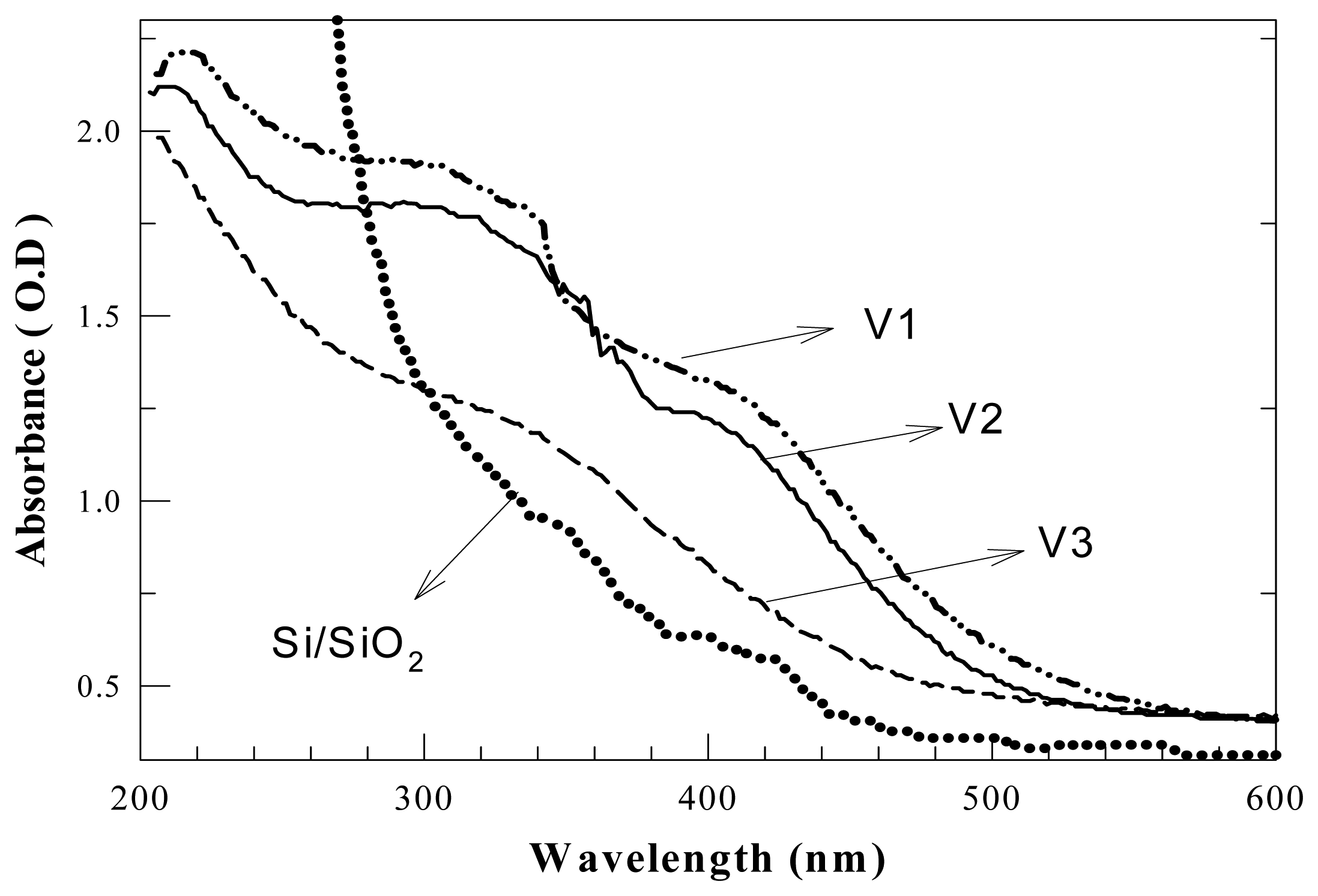
2 sample however, the sensitivity as well as the absorption profile depend on the oxygen flow during growth process. As shown in
Fig.1, from curve V1 to V3 the absorption varies with oxygen flow rate decreased. In general, vanadium may exist as V
0(metallic), V
2+, V
3+, V
4+ and V
5+. V3 sample prepared with minimum amount of oxygen contains mostly metallic vanadium. The absorption curve only shows a shoulder at ∼320 nm with absorbance of 1.4 OD, corresponding to the cut-of-edge of quartz silica (CT band). For V1 sample, it was prepared with moderately higher oxygen flow than V2 sample, and it has higher UV absorbance. X-ray diffraction shows a distinct peak at around 28E (011) for monoclinic VO
2. The test on thermochromic effect also showed a better thermochromic effect. It is interesting to note that there are distinguishable double bands observable at 340 nm and 420 nm respectively. Presumably they are associated with Jahn-Teller splitting of the
d orbital of V
4+ ions in distorted octahedral site with
Δ estimated to be 26,300 cm
−1. It indicates that the oxygen deficiency was still expected during V1 sample growth, so that some V
4+ might be present in the film as interstitial ions.
c-Si/SiO
2 thin films show a high sensitivity to UV light. The cut-of-edge is around 280 nm with the absorbance higher than 2.5 OD. It is corresponding to the optical transition from valence band (VB) of the nanocrystal Si to the conduction band (CB) with the bandgap in average of 2.7 eV [
4].
UV-induced Photoluminescence
Photoluminescence (PL) measurement for VO2 thin films was carried out using pulsed Nd:YAG lase operating at 355 nm. A broadband emission with the band maximum at ∼ 590 nm was observed. This emission can be assigned to 2T2- 2A2 transition of V4+ (3d1). The photoluminescence decay shows a lifetime of about 3 μs. In addition to 355 nm excitation, the PL was also examined at 532 nm excitation. It was found to be very sensitive to the excitation intensity, and was believed to be two-photon absorption (TPA) in nature. Using CW light source a similar PL pattern was also obtained. Therefore the VO2 thin film samples are sensitive only to the UV region.
The PL of c-Si/SiO
2 samples were also examined with the interest in steady photoemission behavior as well as in dynamical processes of excited state upon laser excitation. In order to obtain information of energy gap and excited state dynamics, Eu
3+ ions were introduced as the sensitive probe. The steady PL was measured using a CW Ar
+ laser operated at UV 458 nm as well as at 488 nm. As discussed above that the sample was very sensitive to UV light, the strong PL with a band maximum at ∼ 590 nm was observed.
Fig.2 shows a characteristic Eu
3+ emission peak at 625 nm overlapped with the broadband emission from c-Si/SiO
2. Using pulsed Nd:YAG laser (pulse duration 30 ps) operated at 355, or at 532 nm by two-photon absorptiuon (TPA), all PL components from different origin were identified.
Photoluminescence From Eu3+-Prob
Trivalent Eu
3+ ions doped solid state materials have always received special interest among those incorporating with rare-earth ions. This is due to the sensitive Eu
3+ ions, which can be used as a structure probe. In this study we observed strong coupling between Eu
3+ and nanocrystal-Si, which results in immediate capture of photogenerated charge carriers in conduction band of c-Si by trivalent europium Eu
3+ ions. Accordingly, transient valence switching from trivalent Eu
3+ to divalent Eu
2+ occurred in the process of charge transfer. The excitation of created Eu
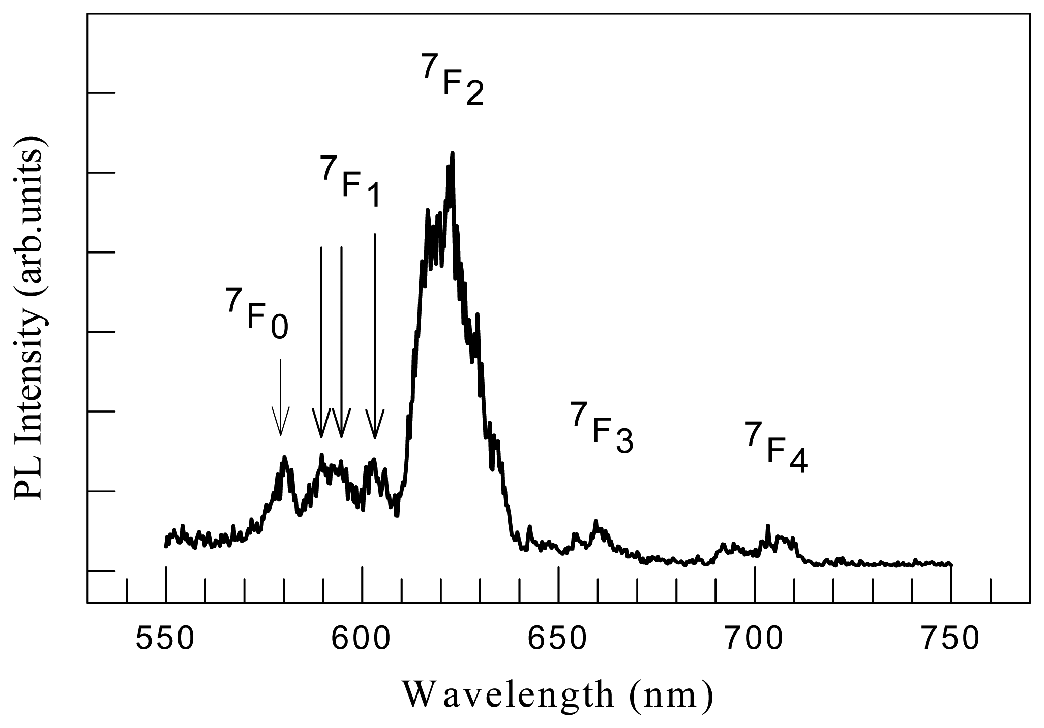
2+ ions was through TPA, giving a broad luminescence with a band maximum at ∼560 nm. A set of Eu
3+ emission was identified by observing a group of well separated peaks using time-resolved technique in the region between 570nm and 720nm. As shown in
Fig.3 those are radiative transitions from metastable
5D
0 level to ground state
7F
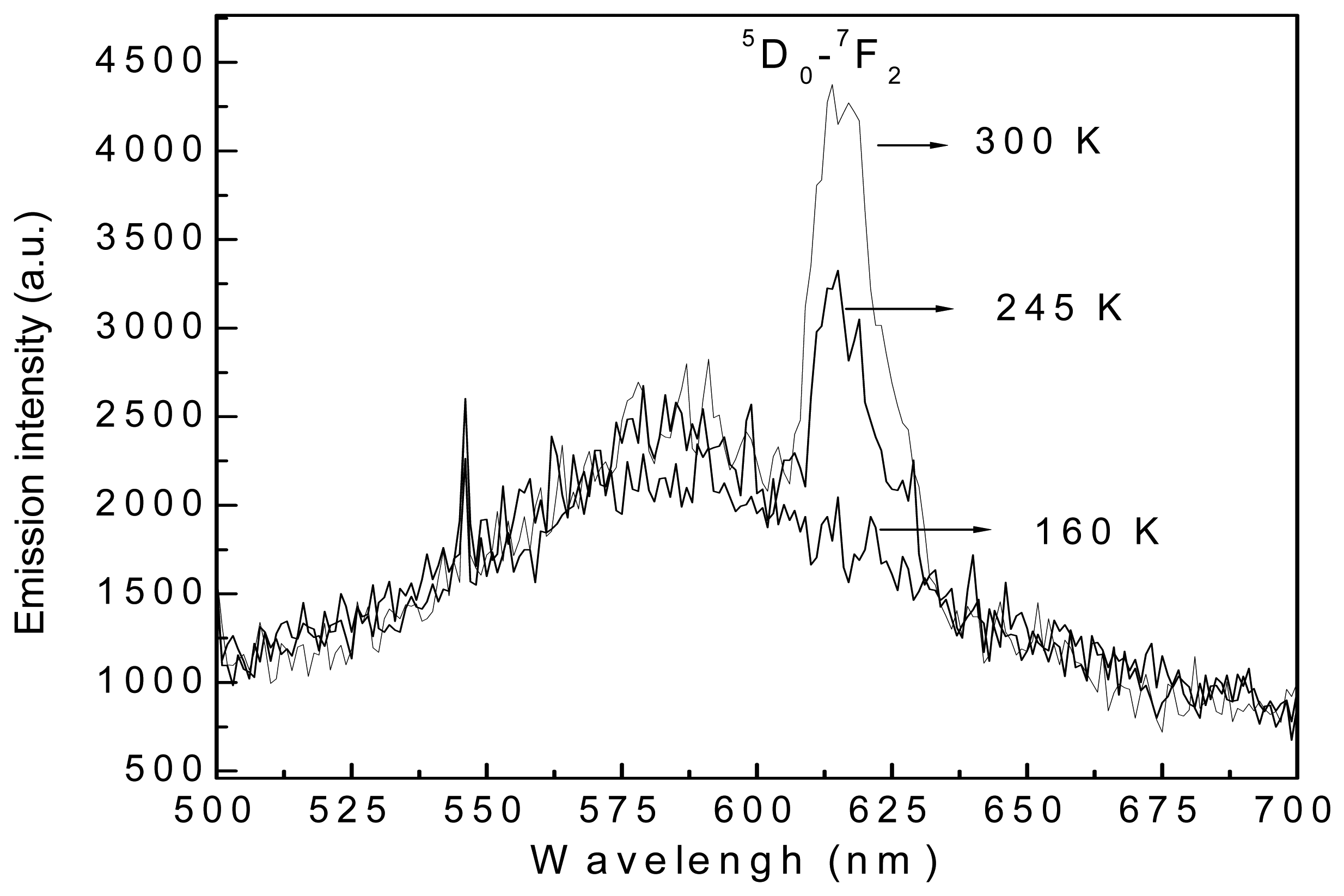
j with j = 0, 1, 2, 3, 4. The temperature dependence of PL shows that the Eu
3+ emission becomes weaker when the temperature was going down, and it was completely quenched at 110 K.
According to the previous studies on the correlation of luminescence and nanoparticle size [
4,
5], higher annealing temperatures result in smaller particles and less variation in size at each position and overall. In this experiment, annealing the as-sputtered Si/SiO
2 at 1100°C results in Si nanoparticles with average sizes ranging from about 1 to greater than 3nm, with the dominant sizes ranging from about 1.0 to 2.1 nm. Annealing should help crystallization and other bond formation processes, and perhaps nanoparticle growth, but some oxidation could also take place with O
2 from the atmosphere (or, in the Eu-doped samples, from the Eu
2O
3).
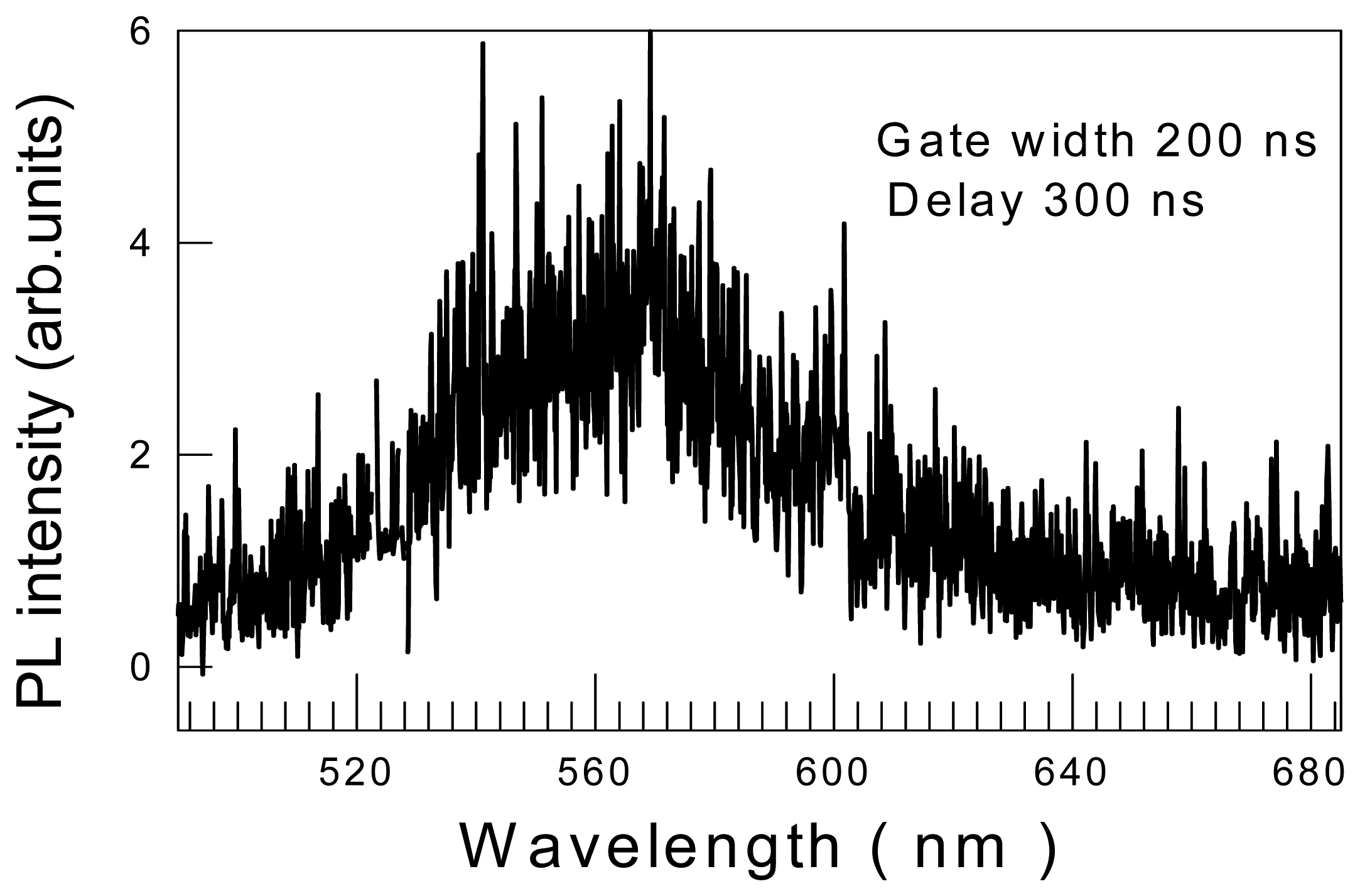
As mentioned above, a broadband Eu
2+ emission was also observed when using pulsed UV excitation or through TPA. The emission peak is at ∼ 560 nm with a FWHM of ∼ 2900 cm
−1 as shown in
Fig.4. The lifetime of this broadband emission was measured to be ∼ 0.8 μs, about 2 orders of magnitude longer than that of c-Si/SiO
2 host emission, but ∼3 orders of magnitude shorter than Eu
3+ emission. This PL has a large part of spectral profile overlapped with the broadband host PL, and the Eu
3+-PL as well. However, its characteristic emission [
7-
9] can be recognized and identified using time-resolved technique from other PL origins. It is interesting to point out that Eu
2+ emission was not observable in the sample where no c-Si nanoparticles exist. In other words, the observation of Eu
2+ emission is associated with the existence of c-Si nanoparticles, through which Eu
3+ - Eu
2+ switching can be realized during excitation process [
10].
Ultrafast Nonlinear Optical Response
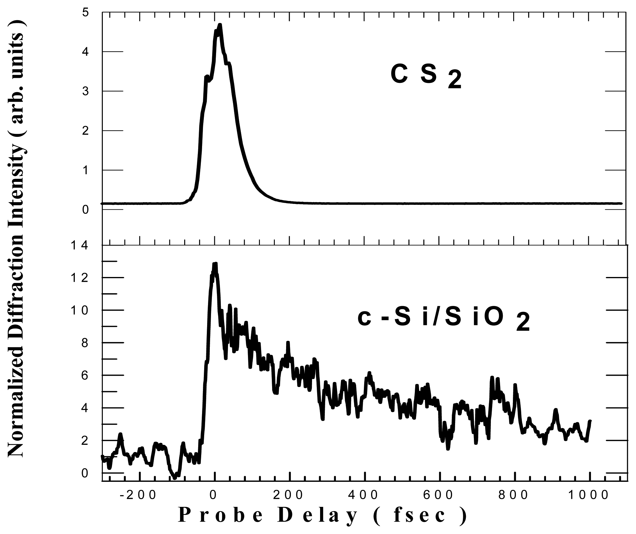
The ultrafast nonlinear optical response was examined using dynamic holography in a degenerate-four-wave-mixing (DFWM) configuration. The holography was produced by cross-over of two coherent ultrashort laser pulses as shown in
Fig. 5. The generated excited state grating is sensed by a third probe pulse. The diffracted signal by transient grating gives more information on the excited state dynamics. A fs- or ps-laser system was used. As shown in
Fig. 5, a sophisticated optical delay line of 15 fsec accuracy was used (s-polarized), which may give information as fast as in femtosecond time scale. The “zero delay” was defined in such a way that the temporal and spatial overlap of the three beams at zero delay time will in principle result in maximum instantaneous response signal when a CS
2 standard is used. The signal observed at the delay time greater than zero is defined as post-zero signal. When the holographic pattern produced by the interference of the two equally divided crossing pulse with crossing angle of
2θ and each with light intensity
I, the transient grating due to the light intensity modulation is formed by
I=
2I [1+
cos(qx)] for (ss) polarizations. In the bright area of the interference pattern the light-matter interaction results in the population of excited state, which consequently causes the change in polarizability of excited state versus ground state. The grating vector is
q= ± (
kA −
kB) confined in the film, where
kA,
kB stand for the wavevector of pulse A and B, respectively. The signal obtained is associated with the change in index of reflection as
Δn= [
Δn
10(
I)cos
kx]
t=0+ [
Δn
20e
−t/℧cos
kx]
t>0+
Δn
30cos
(kx) (1−cos
ωt), where
k,
℧ and
ω are the grating wavevector, excited state relaxation time and phonon frequency, respectively. The coefficients
Δn
10,
Δn
20 and
Δn
30 are the pump intensity dependent amplitudes of refractive index changes arising from different interactions. The first term is responsible for the instantaneous (t=0) contribution to the scattered signal, arising from the χ
(3) including resonant enhancements. The second term allows for the scattering of the probe at time delay longer than the autocorrelation width of the three beams and arises from changes in polarizability due to excited state population. The last term account for changes in the index of refraction due to laser induced acoustic waves.
Ultrafast Response in VO2 Thin Films
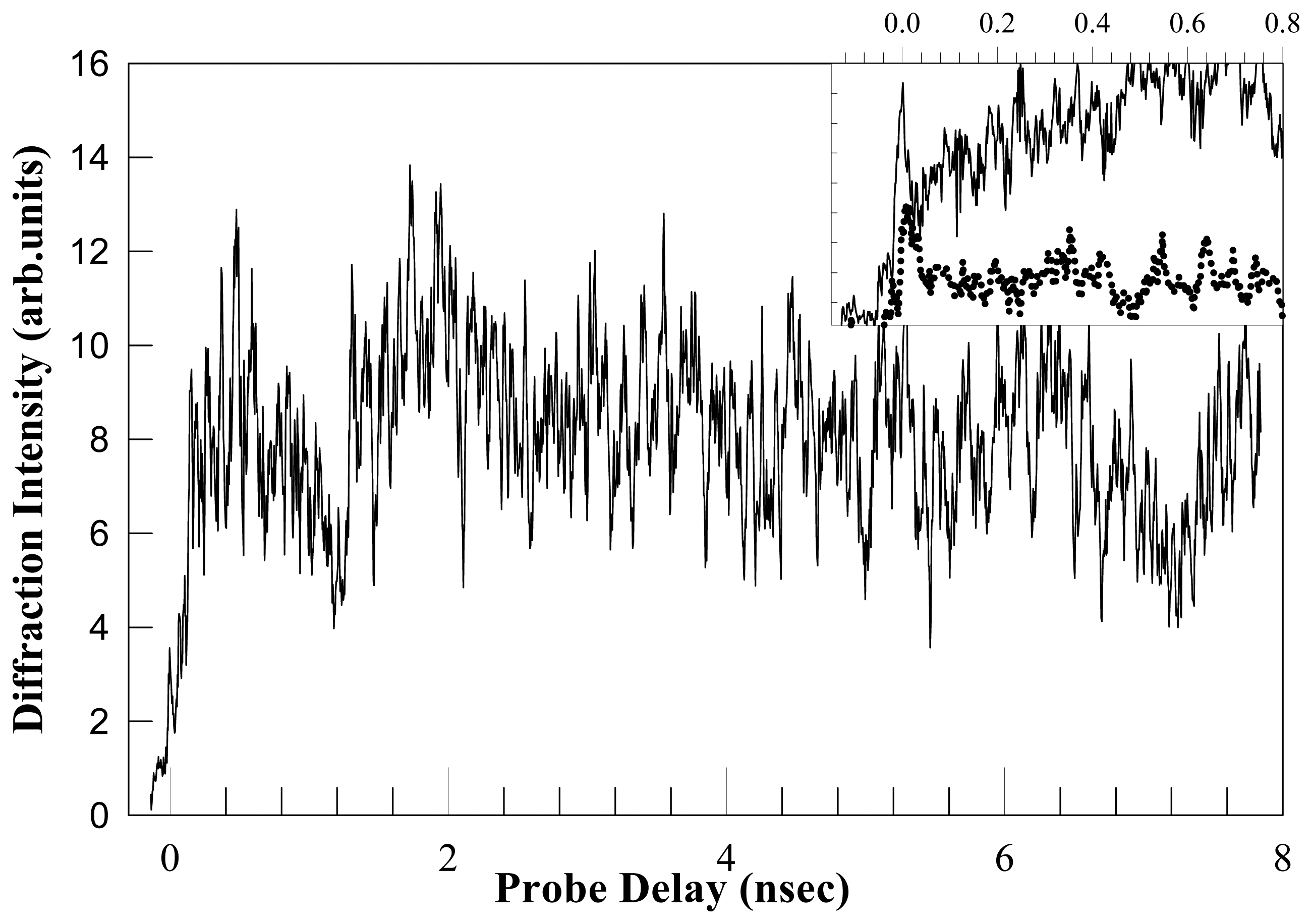
Figure 6 represents a time-resolved, transient holography which is plotted as diffracted signal versus the time delay for a PLD-VO
2 film deposited on a fused quartz substrate. It clearly shows the excited state dynamic process of VO
2 film, which was induced by optical excitation. In the inset a sharp peak signal at zero probe delay represent an intrinsic optical response which is associated with the third-order susceptibility of the material. The signa post-zero delay represents the transient grating produced by laser excitation of VO
2 film coupled to its excited states [
11]. The signal reaches its maximum value at ∼0.6 nsec. There is a distinguishable signal damping down at 1.2 nsec forming a dip in the profile. This observation was reproducible in over hundreds measurements as long as the pump fluence was kept moderately low. It was also excluded from acoustic phonon contribution by theoretical analysis as well as by experimental verification.
Since the observed post-zero signal (proportional to the square of the change in polarizability) is even 3.2 times greater than the intrinsic response at zero-delay the lattice displacement is estimated to be quite a significant. As the lattice parameters changes dramatically prior or after PT point [
12,
13], a large change of lattice constant along c-axis was found to be associated with the phase transition from semiconductor to metallic state. Therefore it suggests that the laser induced phase transition is the cause giving rise to such an intense post-zero grating signal. Furthermore, the evidence from experiment conducted at the temperature over 68EC shows that (in the inset of
figure 6, dotted line), there was no grating signal observed because the VO
2 film was already in a metallic phase before laser excitation. Therefore all these observations propose that the observed transient holography in the VO
2 thin film is associated with the excited state dynamical process which essentially causes the structural change, or so-called optically induced-PT. Regarding the signal drop down at 1.2 nsec forming a dip in the profile, it is believed to be due to an unknown middle state bridging the semiconductor and metallic phase.
Ultrafast Response in c-Si/SiO2 Thin Films
Based on the optical measurements, the VB - CB energy gap of c-Si nanoparticles is estimated to be ∼ 3.0 eV. Upon an intense laser excitation at 355 nm or by two-photon absorption at 532 nm, photoinduced charge carriers are expected to be easily produced in CB. These carriers are moving around and might be trapped at some defect sites to form so-called shallow centers.
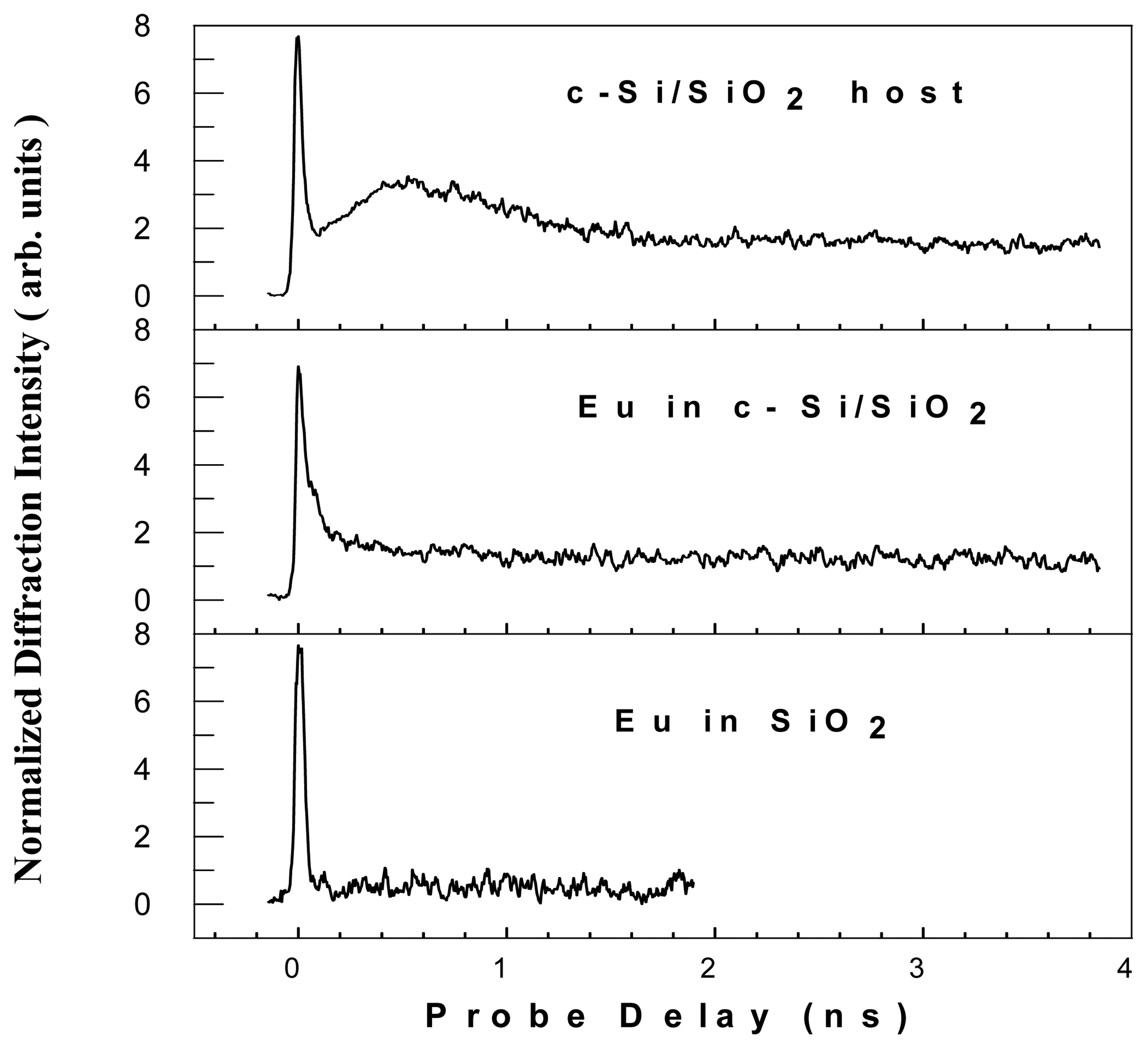
Fig.7 shows the ultrafast optical response signal of samples versus probe pulse delay. The signal at zero-delay was extremely strong. In nondoping nanoparticle c-Si/SiO
2, upon laser excitation the signal post-zero delay features an intensity buildup, reaching the maximum at the delay time of about 400 ps. It decays slowly thereafter with a long-lasting tail extending out of the scale. In Eu
3+-doped nanoparticle c-Si/SiO
2 sample, however, this kind of alteration of the SR signal right after the instantaneous response was not observed.
In the doped sample it features a slowly decaying signal with an average decay rate of 2×10
8/s, which corresponds to a half of the luminescence lifetime of nanoparticles (∼10 ns as discussed above). It is interesting and important to understand the physics behind these observations. From luminescence study these trapped sites are likely to be shallow centers which may be reactivated by excitation. It will also modify the susceptibility of CB versus VB. The change in susceptibility χ
(3) is related to)
n. The diffracted signal intensity
0 =
exp.
(-
d/
cos2) sin2 (d)n /
8cos2), which is related to)
χ, and)
n =
(12B/
n0<
E2>
) χ(3),
E is the optical electric field. The enhancement of the instantaneous response signal (at zero-delay) was significant. When each pump pulse was at 1.2 μJ, the observed diffraction efficiency reached 6.8 × 10
−3. A significantly high sensitivity to the UV with the third-order susceptibility χ
(3) of 1.1 × 10
−10 esu was obtained in comparison to the previous value of 6×10
-12 esu for regular silicon material [
14].
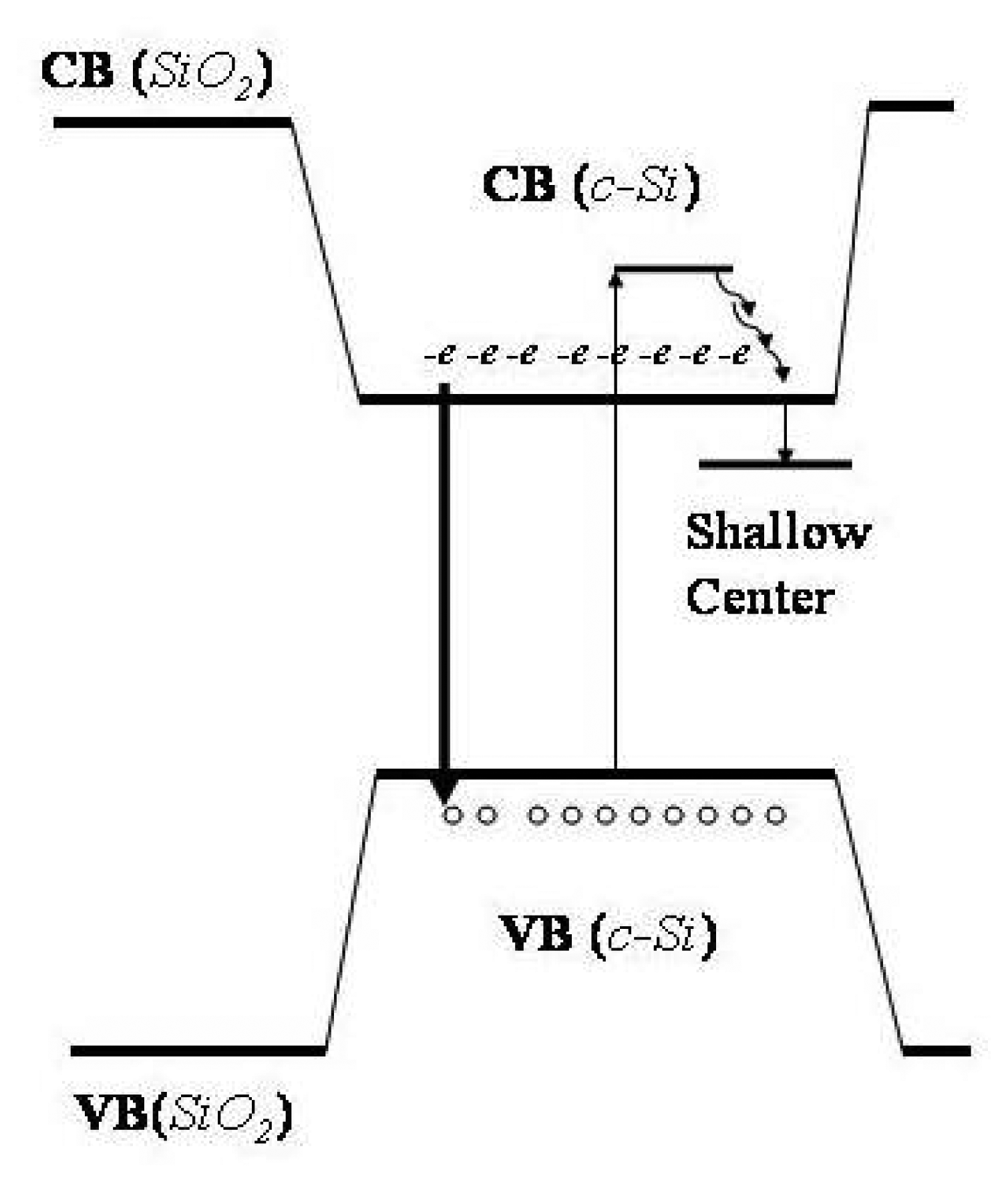
Based on the above observations a model of structure of Eu-doped nanoparticle c-Si/SiO
2 can be represented as shown in
Fig. 8. Nanoclusters of silicon in the SiO
2 matrix are under the essential random defect fields with atom-scale size. As a result, the bottom of Si-nanoparticle conduction band (which is assumed approximately corresponded to k
i ∼ 0.85 k
max, as in the perfect crystal due to multi-valley structure of silicon conduction band) is under the action of strong atomic scale spatial fluctuations. Note that ∼20Δ size of Si nanoparticle is enough for formation of the bottom of conduction band similar to the perfect Si-matrix. The latter is connected with its minimum at k
i ∼ 0.85 k
max. Only k-values satisfying k < (B/L) inequality, where L is the size of nanoparticle, corresponded to principally different states for the nanoparticle case. The fluctuations induce the spatial multi-well atom-scale structure of conduction band edge. As shown in
Fig. 9, the latter gives rise to conduction electrons localization in these wells and is accompanied by rather slow hopping diffusion of conduction electrons in such wells system.
This model allows explanation of slow diffusion of conduction photoelectrons detected in the experiment for Si-nanoparticles in SiO2 matrix without Eu impurity doping. When Eu3+ impurity ion is located in the interface region of Si-nanoparticle embedded in the SiO2-matrix, it acts as an attractive Coulomb center for the photoelectron. The center will be the core of the localized electronic state. The energy gap between conduction and valence bands for the Si-nanoparticle is much less than for the SiO2 matrix. Electrons and holes both are within a deep potential well in the region of nanoparticle.


