Fabrication and Characterisation of GaAs Gunn Diode Chips for Applications at 77 GHz in Automotive Industry

Abstract
:Introduction
Experimental
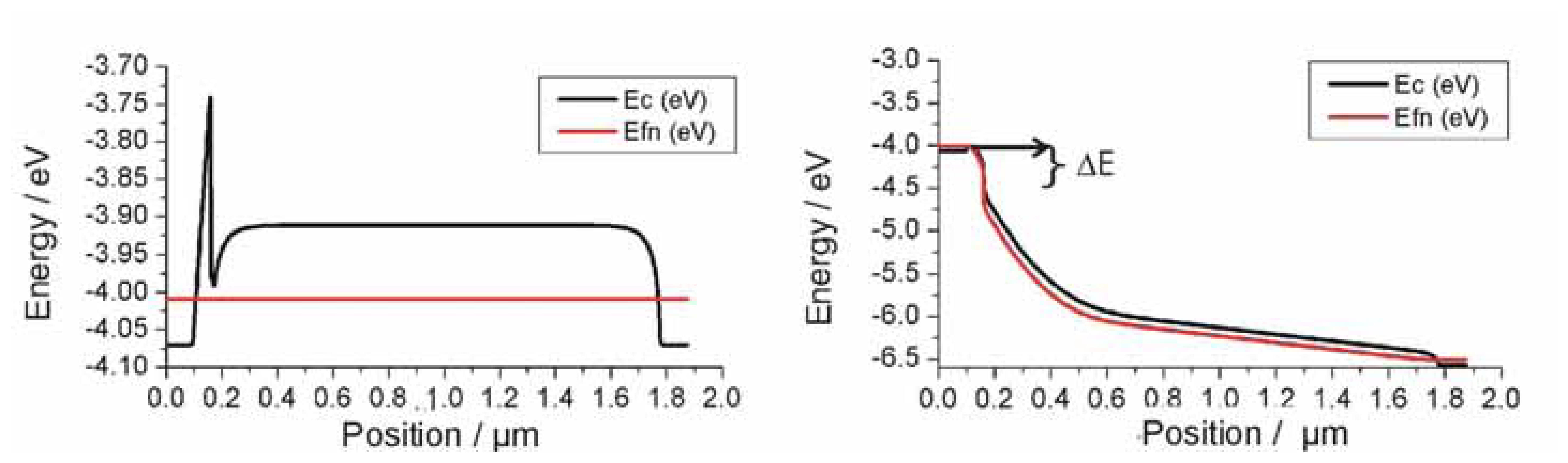
Layer structure
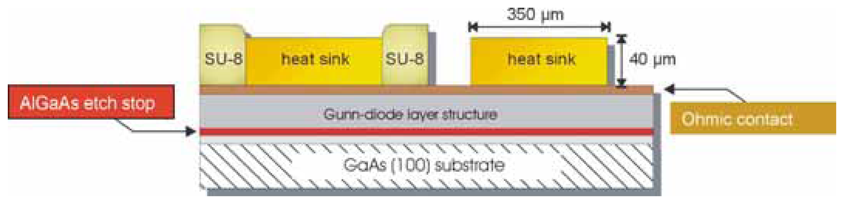
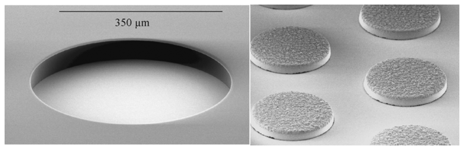
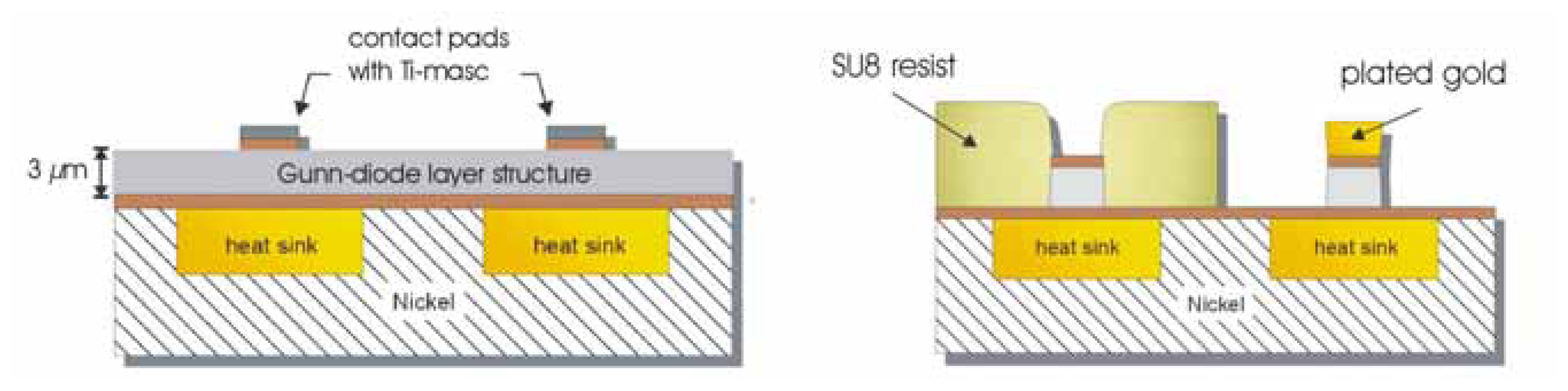
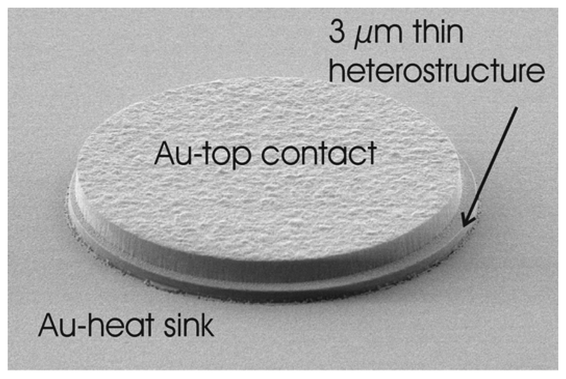
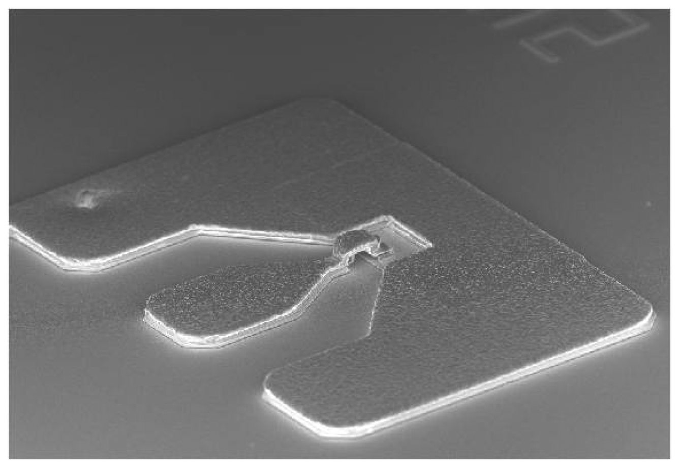
Gunn diode chip processing
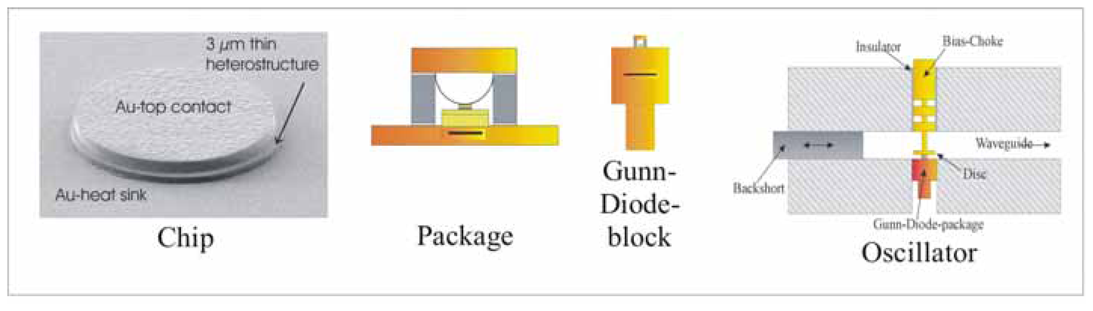
Gunn diode chip packaging and mounting in an oscillator
Planar Gunn diode chip processing
Results and discussion
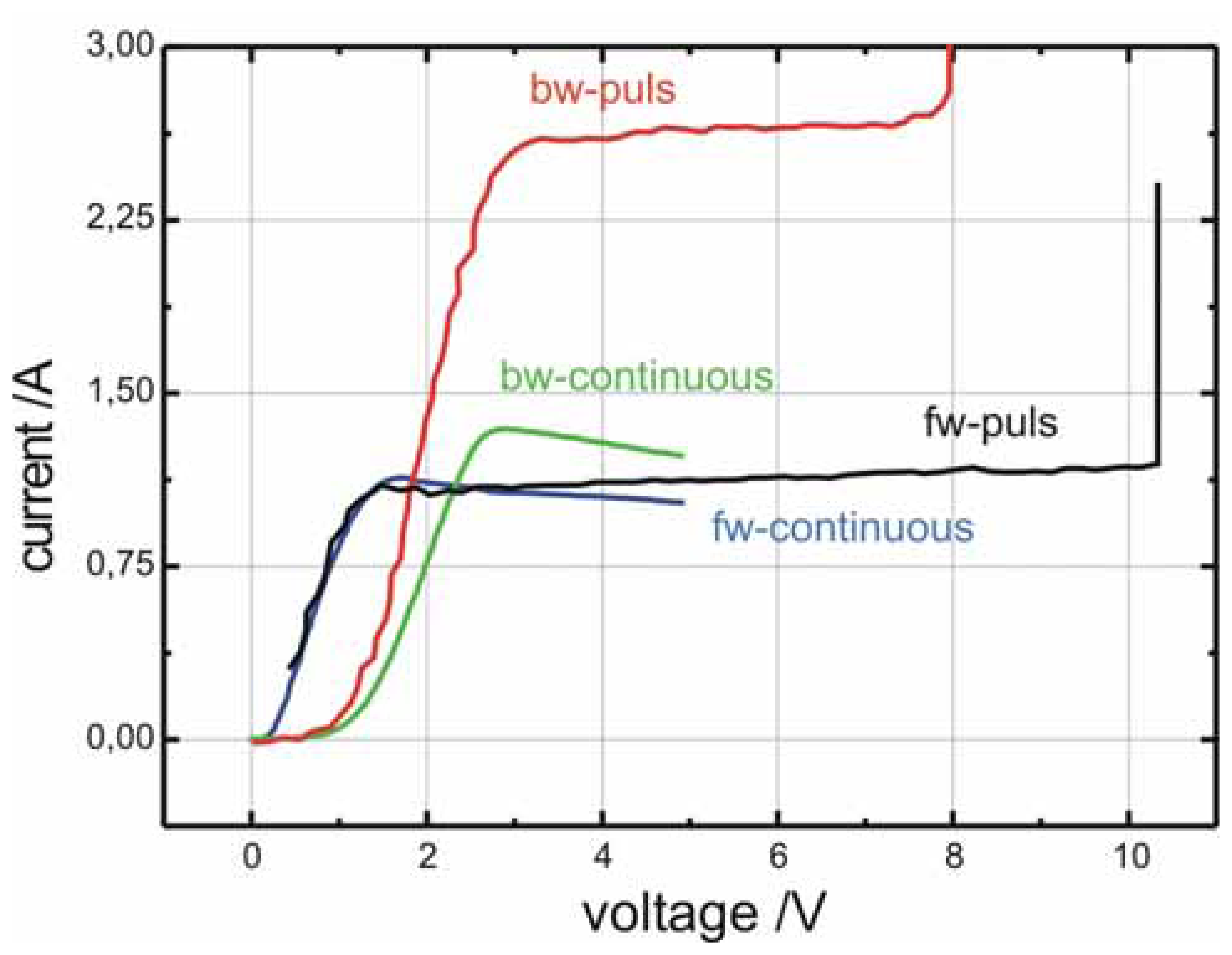
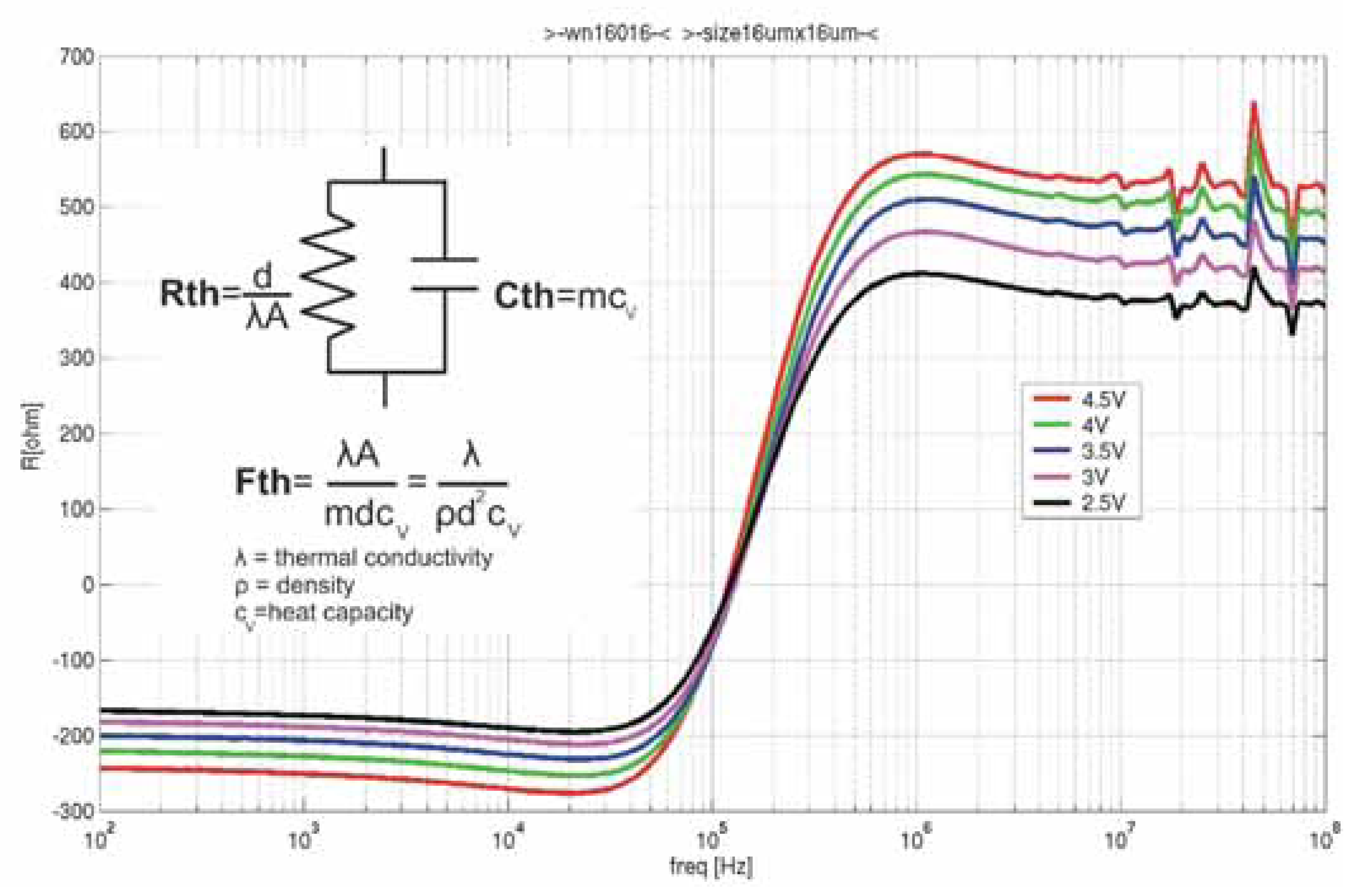
DC and impedance measurements, the heat distribution
High frequency results
Conclusions
References
- Gunn, J.B. Microwave oscillations of current in III/V semiconductors. Solid State Commun. 1963, 1, 88. [Google Scholar]
- Gunn, J.B. Instabilities of current and of potential distribution in GaAs and InP. In Proc. Plasma Effects in Solids; Dunod: Paris, 1965; p. 199. [Google Scholar]
- Hutchinson, S.; Stephens, J.; Carr, M.; Kelly, M.J. Implant isolation scheme for current confinement in graded-gap Gunn diodes. Electron. Lett. 1996, 32, 851. [Google Scholar]
- Couch, N.R.; Beton, P.H.; Kelly, M.J.; Kerr, T.M.; Knight, D.J.; Ondria, J. The use of linearly graded composition AlGaAs injectors for intervally transfer in GaAs: Theory and experiment. Solid-State Electron 1988, 31, 613. [Google Scholar]
- Neylon, S.; Dale, I.; Spooner, H.; Worley, D.; Couch, N.; Knight, D.; Ondria, J. State-of-the-art performance millimetre wave gallium arsenide gunn diodes using ballistically hot electron injectors. IEEE 1989 MTT-S International Microwave Symposium Digest 1; 1989; p. 519. [Google Scholar]
- Stock, J. Herstellung und Charakterisierung von GaAs Gunn-Dioden für Anwendungen bei 77 GHz. PhD thesis, University of Aachen RWTH, 2003. [Google Scholar]
- Montanari, S. Fabrication and characterisation of planar Gunn diodes for Monolithic Microwave Integrated Circuits. PhD thesis, University of Aachen RWTH, 2005. [Google Scholar]
- Cords, H.; Förster, A. Berechnung der Temperaturverteilung in einer Gunn Diode; Technical report; Forschungszentrum Jülich GmbH; FZJ-ZAT-371; 2002. [Google Scholar]
- DeSalvo, G.C.; Tseng, W.F.; Comas, J. Etch rates and selectivities of citric acid/hydrogen peroxide on GaAs, Al0.3Ga0.7As, In0.2Ga0.8As, In0.53Ga0.47As, In0.52Al0.48As and InP. J. Electrochem. Soc. 1992, 139, 831. [Google Scholar]
- Wu, X.S.; Coldren, L.A.; Merz, J.L. Selective etching characteristics of HF for AlxGa1-xAs/GaAs. Electron. Lett. 1985, 21, 558. [Google Scholar]
- Franz, G.; Rinner, F. Reactive ion etching of GaN and GaAs: Radially uniform processes for rectangular, smooth sidewalls. J. Vac. Sci. Technol. A 1999, 56. [Google Scholar]
- Montanari, S.; Förster, A.; Lepsa, M.I.; Lüth, H. High frequency investigation of graded gap injectors for GaAs Gunn diodes. Solid-State Electron. 2005, 49, 245. [Google Scholar]


| 500 nm | GaAs | n=5E18cm-3 | contact layer |
| 10 nm | GaAs | - | spacer layer |
| 50 nm | GaAs → AlxGa1-xAs | - | AlGaAs injector |
| 10 nm | GaAs | - | spacer layer |
| 5 nm | GaAs | n=1E18cm-3 | delta doping |
| 1.6 μm | GaAs | n=1E16cm-3 | Gunn drift zone |
| 500 nm | GaAs | n=5E18cm-3 | contact layer |
| 500 nm | Al0.6Ga0.4As | - | etch stop layer |
| 50 nm | GaAs | - | buffer |
| Substrate | |||
© 2006 by MDPI ( http://www.mdpi.org). Reproduction is permitted for non-commercial purposes.
Share and Cite
Förster, A.; Stock, J.; Montanari, S.; Lepsa, M.I.; Lüth, H. Fabrication and Characterisation of GaAs Gunn Diode Chips for Applications at 77 GHz in Automotive Industry. Sensors 2006, 6, 350-360. https://doi.org/10.3390/S6040350
Förster A, Stock J, Montanari S, Lepsa MI, Lüth H. Fabrication and Characterisation of GaAs Gunn Diode Chips for Applications at 77 GHz in Automotive Industry. Sensors. 2006; 6(4):350-360. https://doi.org/10.3390/S6040350
Chicago/Turabian StyleFörster, Arno, Jürgen Stock, Simone Montanari, Mihail Ion Lepsa, and Hans Lüth. 2006. "Fabrication and Characterisation of GaAs Gunn Diode Chips for Applications at 77 GHz in Automotive Industry" Sensors 6, no. 4: 350-360. https://doi.org/10.3390/S6040350