Article

Micro Semiconductor CO Sensors Based on Indium-Doped Tin Dioxide Nanocrystalline Powders

1
Department of Electronics Engineering, Chungnam National University, Daejeon, South Korea
2
Optic and Electric Materials Center, Korea Institute of Energy Research, Daejeon, South Korea
*
Authors to whom correspondence should be addressed.
Sensors 2006, 6(5), 526-535; https://doi.org/10.3390/s6050526
Submission received: 10 March 2006 / Accepted: 10 May 2006 / Published: 10 May 2006
(This article belongs to the Special Issue Gas Sensors)

Abstract

:
The precursors of SnO2 or In2O3/SnO2 nanocrystlline powders have been prepared by the sol-precipitation method. The precursors were calcined at different temperatures to prepare SnO2 or In2O3/SnO2 nanocrystalline powders with different particle sizes. The nanocrystallites were examined by differential thermal analysis (DTA), X-ray diffraction (XRD) and transmission electron microscopy (TEM). And then thick film CO sensors were fabricated using prepared SnO2 or In2O3/SnO2 nanocrystlline powders loaded with PdOx. The composition that gave the highest sensitivity for CO was in the weight% ratio of 5 wt.% In2O3/SnO2:PdOx as 99:1(wt %). The composite material was found sensitive against CO at the working temperature 200 °C. It was found that the sensors based on In2O3/SnO2 nanocrystalline system exhibited very short response time to CO at ppm level. These characteristics make the sensor to be a promising candidate for detecting low concentrations of CO.

Introduction

In recent years, great attention has been paid to nanometresized materials in studies of their fundamental mechanism, such as the size effect and the quantum effect, and in applications of these materials [1, 2]. Tin dioxide powders or indium-doped tin dioxide powders are used in many different applications, such as microelectronics, solar cells, semiconductor gas sensors, electroluminescence, etc.
The SnO2 powders are usually prepared from α- or β- stannic acid, followed by a calcining process, which seems to affect the properties of the powders more extensively than other processes. Therefore, exploration of the calcining effect on the properties of SnO2 powder may provide valuable information for sensors, solar cells and electroluminescence [3-5].
Tin dioxide or indium doped tin dioxide is the most used n-type semiconductor in gas sensing devices because of its capabilities to detect inflammable gases like CH4, H2, C2H5OH, CO and so on [6-16]. This material, when exposed to atmosphere, is inclined to physisorbe oxygen molecules, pick up electrons from the conduction band of SnO2 [17], create a positive space-charge layer just below the surface of SnO2 particles, lift the potential barriers between the particles and lower the electrical conductance of the SnO2 film. Reducing gases, such as H2, CH4, C3H8, C2H5OH or CO, react with the physisorbed oxygen [18] by increasing the electron concentration in the material, thereby decreasing the electrical resistance. This change in resistance serves as sensing signal. The main drawback of tin oxide however is its low selectivity towards reducing gases and thus cross sensitivity between these gases is one of the major problems [13, 19].
In this work, the precursors of SnO2 or In2O3/SnO2 nanocrystalline powders were prepared by the sol-precipitation method. The precursors were calcined at different temperatures to prepare SnO2 or In2O3/ SnO2 nanocrystalline powders with different particle sizes. The nanocrystallites were examined by differential thermal analysis (DTA), X-ray diffraction (XRD) and transmission electron microscopy (TEM). And then thick film gas sensors were fabricated using prepared SnO2 or In2O3/SnO2 nanocrystlline powders loaded with PdOx for CO detection.

Experimental

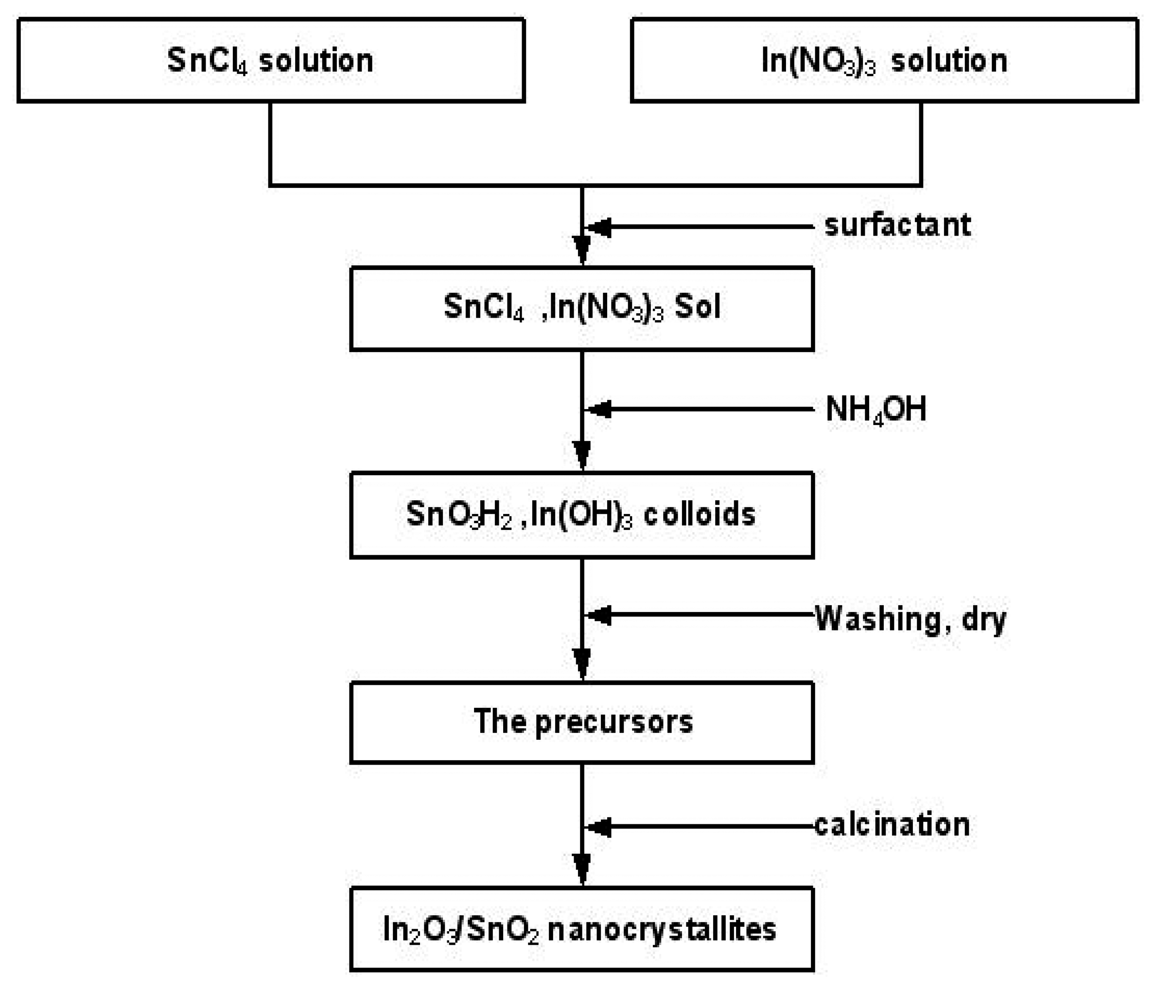
Sensing materials preparation
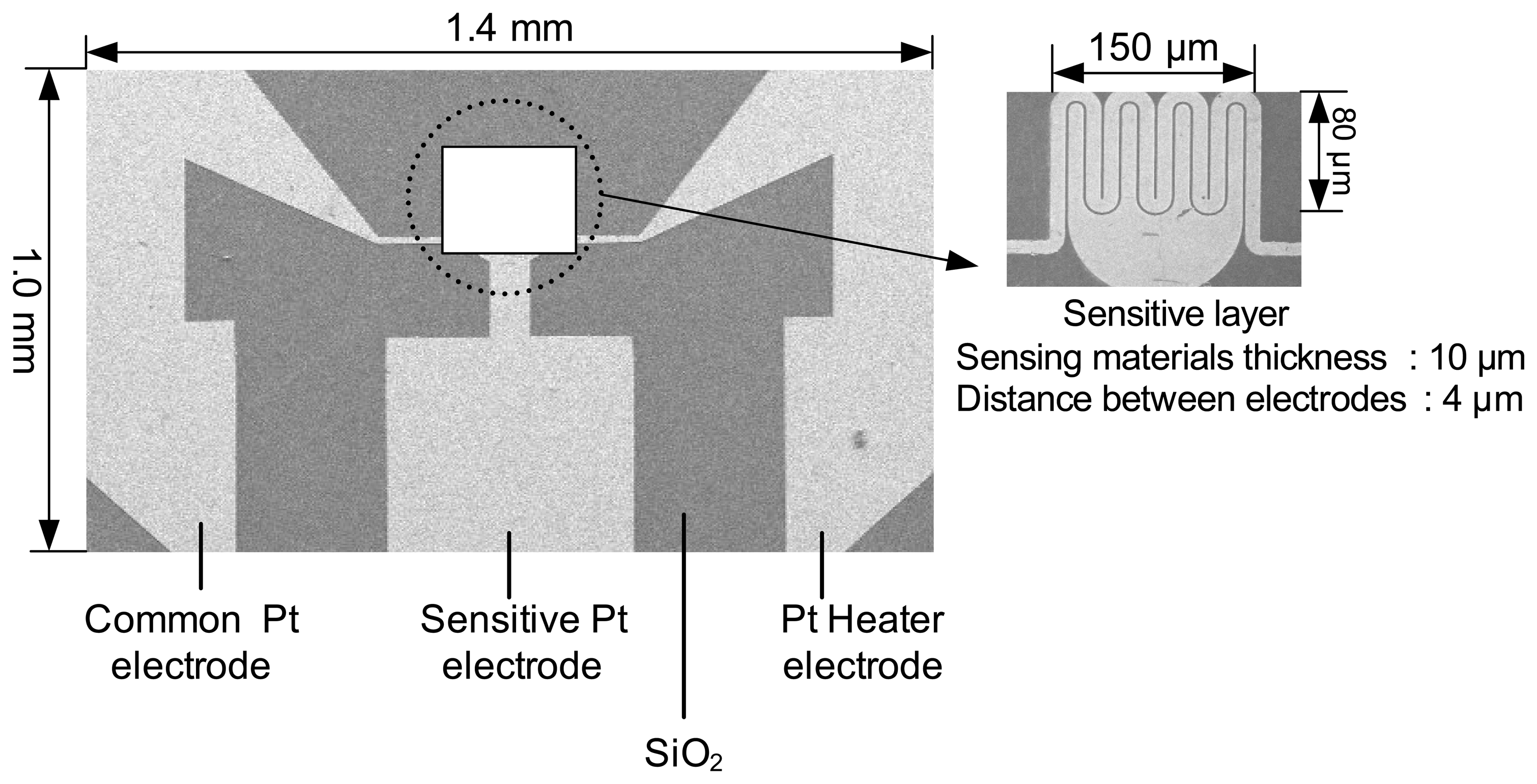
The precursors of tin dioxide nanocrystalline powders or tin dioxide nanocrystalline powders doped with indium oxide (In2O3/SnO2) were prepared by the sol-precipitation method. The reaction conditions, such as the concentration of reactants, the surfactant, pH value, the amount of indium oxide doped, and the reaction temperature and time, were studied. A mixed acidic solution of SnCl4 and In(NO3)3 was made using the Triton X-100 as surfactant, and reacted with aqueous ammonia to form the sol-precipitate of α-stannic acid (SnO3H2) and In(OH)3 at pH < 7.0. The precipitate was washed thoroughly with deionized water, dried at < l00 °C, and ground into powders as the precursors. The precursors were calcined at temperatures from 200 to 900 °C in air for 2 h to produce SnO2 and In2O3/ SnO2 nanocrystalline powders with different average particle sizes. Figure 1 shows the process for preparing In2O3/ SnO2 nanocrystalline powders. The average particle sizes of the nanocrystallites were evaluated from the XRD line of the (101) face based on Scherrer equation. The structural properties and morphology of the In2O3/ SnO2, nanocrystalline powders were characterized by using DTA, XRD, TEM, etc.

Sensor fabrication

The micro gas sensor was fabricated on the silicon substrate with Pt electrode and heater. The fabrication of the silicon based chip was achieved according to the following steps; (a) thermal oxidation of the surface for insulating layer formation, (b) prepatterning for the cavity by wet etching with HF, (c) Cr deposition followed by Pt deposition by thermal evaporation in a chamber, (d) photo-resistive film formation, (e) patterning for the heater and the sensing electrode (Pt electrode), (f) removal of photo-resistive film, (g) wet etching using HF for forming, and (h) screen printing for micro sensitive layer(about 10 μm thickness) using the mixed solution of nano-crystalline SnO2 or In2O3/SnO2 with PdOx, ethyl cellulose(6 wt.%) and silica gel(24 wt.%) binder as mechanical stabilizer. The fabricated silicon-based chip is shown in Figure 2. The dimensions of the chip area are 1.4 mm × 1.0 mm, and its sensitive layer is about 150μm × 80μm. The distance between sensitive electrodes in the chip is 4.0 μm (Figure 2).

Measurement of sensor resistance

All experiments were carried out using an environmental test chamber. The heater temperature was maintained at 200 °C with a supply of heater voltage of ∼1.0 V. The measurement of the sensor temperature was made with the help of IR-0506 (Minolta Corp.) temperature analyzer. All these experiments were done at a fixed humidity of 65%RH. Fresh air with a controlled humidity of 65%RH at 22 °C (room temperature) was led and then the gas inlets and outlets of the chamber were closed. The sensor resistance was measured as the chamber reached at the desirable conditions. This experiment was repeated with different fresh gas and test gas composition. The resistance of the sensor was measured for each composition.

Results and discussion

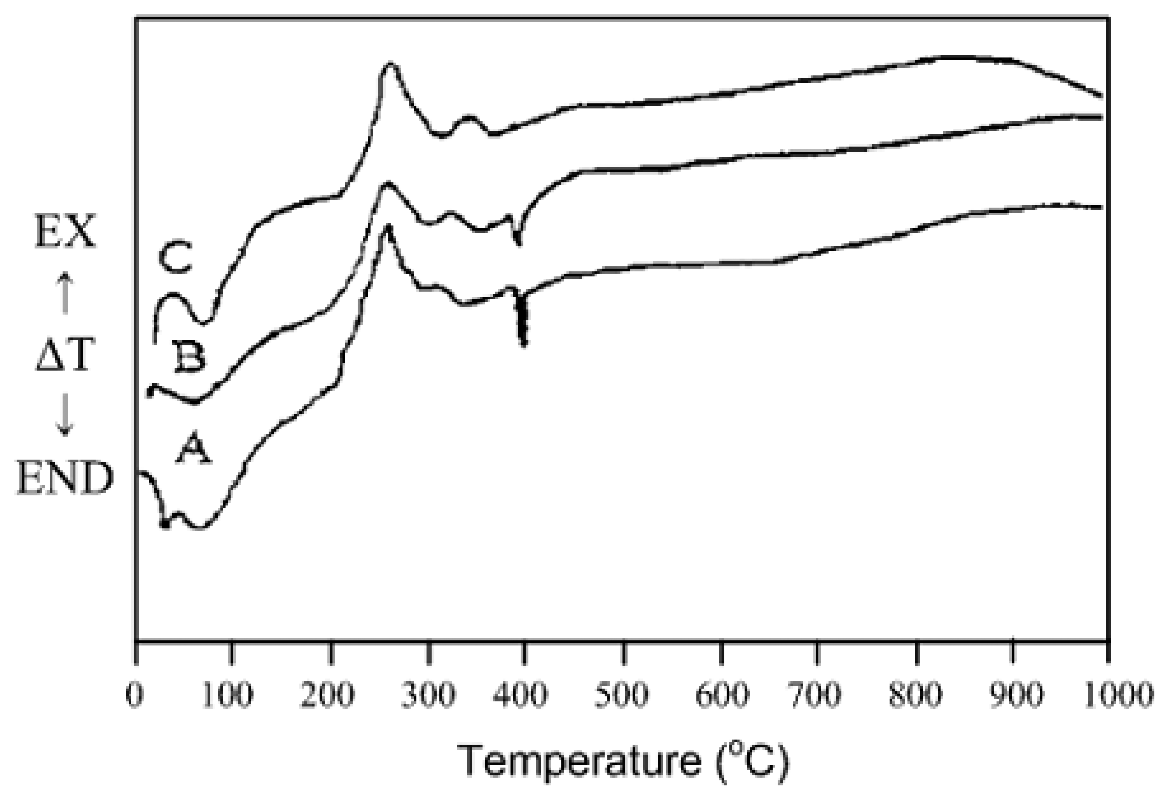
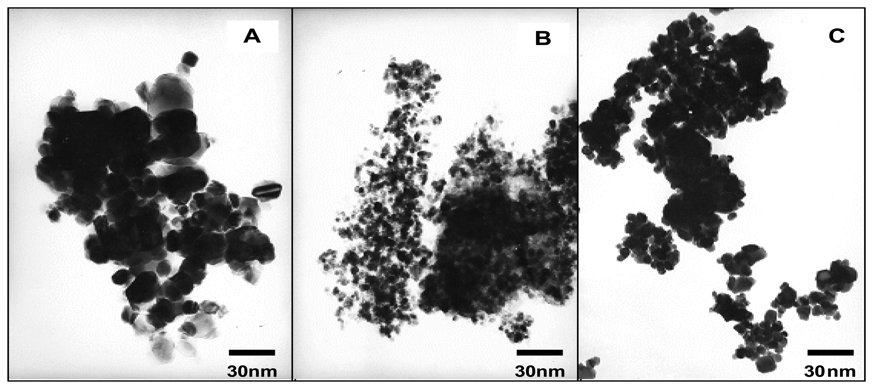
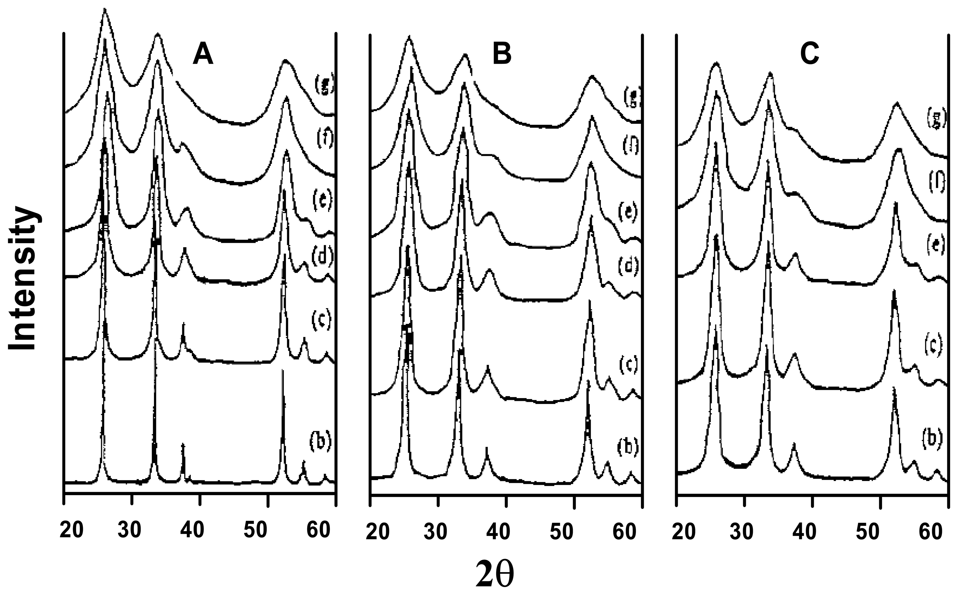
Structural characteristics of sensing materials

The precursors of SnO2 and In2O3/ SnO2 nanocrystaline powders were prepared by the sol-precipitate method. During their preparation, the reaction conditions, such as the concentration of reactants, the surfactant, pH value, the amount of indium oxide doped and the reaction temperature and time were studied through many experiments. The concentrations of SnCl4 solution were 0.05-0.25 M, and those of In(NO3)3 were 0.001-0.01 M. The best condition of reactants was selected from many experiments to prepare samples with the smallest particle size. The quantities of indium oxide doped in the SnO2 powders were 5 and 10 wt.%. A solution with pH < 7.0 was controlled exactly by drops of ammonia hydroxide solution.
The DTA of SnO2 or In2O3/ SnO2 precursors is shown in Figure 3, where the sample A, B and C are SnO2, 5 wt.% In2O3/ SnO2 and 10 wt.% In2O3/ SnO2, respectively.
It is seen that there are several endothermic peaks at 280-400 °C, indicating that tin dioxide powder was formed by dehydration at these temperatures, corresponding to the scheme:
  • SnO3H2→Sn2O5H2→Sn4O9H3→SnO2
Doping with a small quantity of In2O3 does not appear to affect the preparation process of the samples to a great extent. Another endothermic peak at 268 °C was attributed to the surfactant decomposition.
Figure 4 shows TEM images of SnO2 and In2O3/ SnO2 powders calcined at 800 °C for 2 h. It is shown that the particle shape of the samples is spherical. The powders are quite uniform in size and the particle size decreases with increasing doping quantities of In2O3. The result of TEM is consistent with that of XRD.
The XRD patterns of In2O3/ SnO2 nanocrystalline powders with different quantities of doped indium calcined at different temperatures for 2 h in air are shown in Figure 5. In all cases a cassiterite pattern was produced. This was well developed for the sample calcined at high temperatures, corresponding to d-spacing of 0.3348, 0.2643, 0.2369 and 0.1764nm. This is in accordance with the XRD card of SnO2. From the XRD patterns, In2O3/ SnO2 nanocrystalline powders were formed and there is a strong broad band for those calcined at low temperature. The effect of the particle size of the samples with different doped quantities on the calcining temperature is shown in Table1. When the materials (No. g) were heated at 800 for 2h, sharp peaks were obtained corresponding to the cassiterite structure. In the subsequent sensing studies these were used gas sensor as the sensing material.
It is shown that the average particle sizes of samples increase with increasing calcining temperature and the thermal stability of the samples is very strong. The doped quantity of In2O3 was too small to affect the different patterns, even it affected the particle size of In2O3/ SnO2 although the samples were calcined at the same temperature, they differed in the doped quantity of In2O3. The crystal size was found to be similar for samples calcined at low temperature. The crystal size decreases with increasing doped quantity for calcining at or beyond 400 °C. This implies that the doped In2O3 restrains SnO2 from crystal growth.

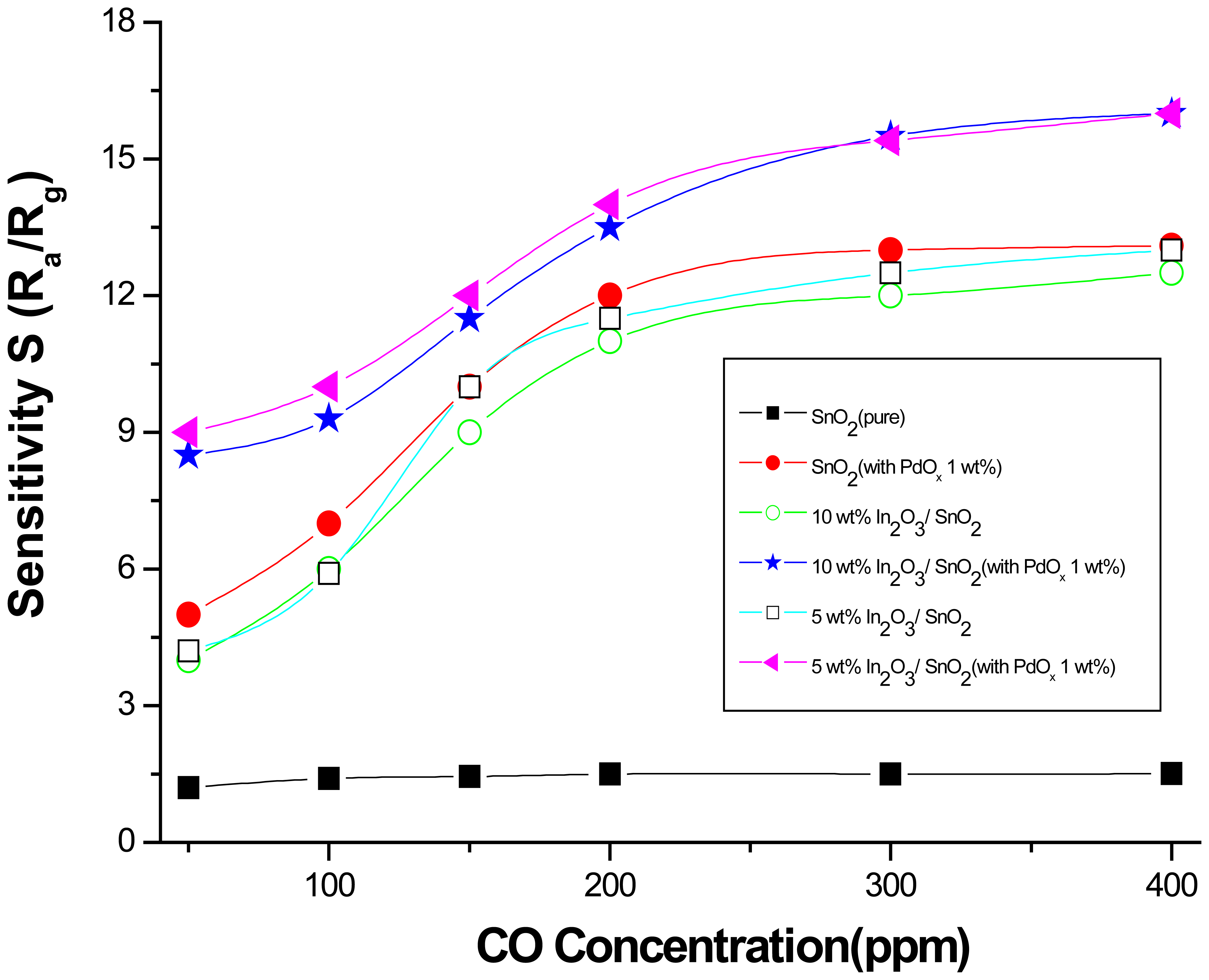
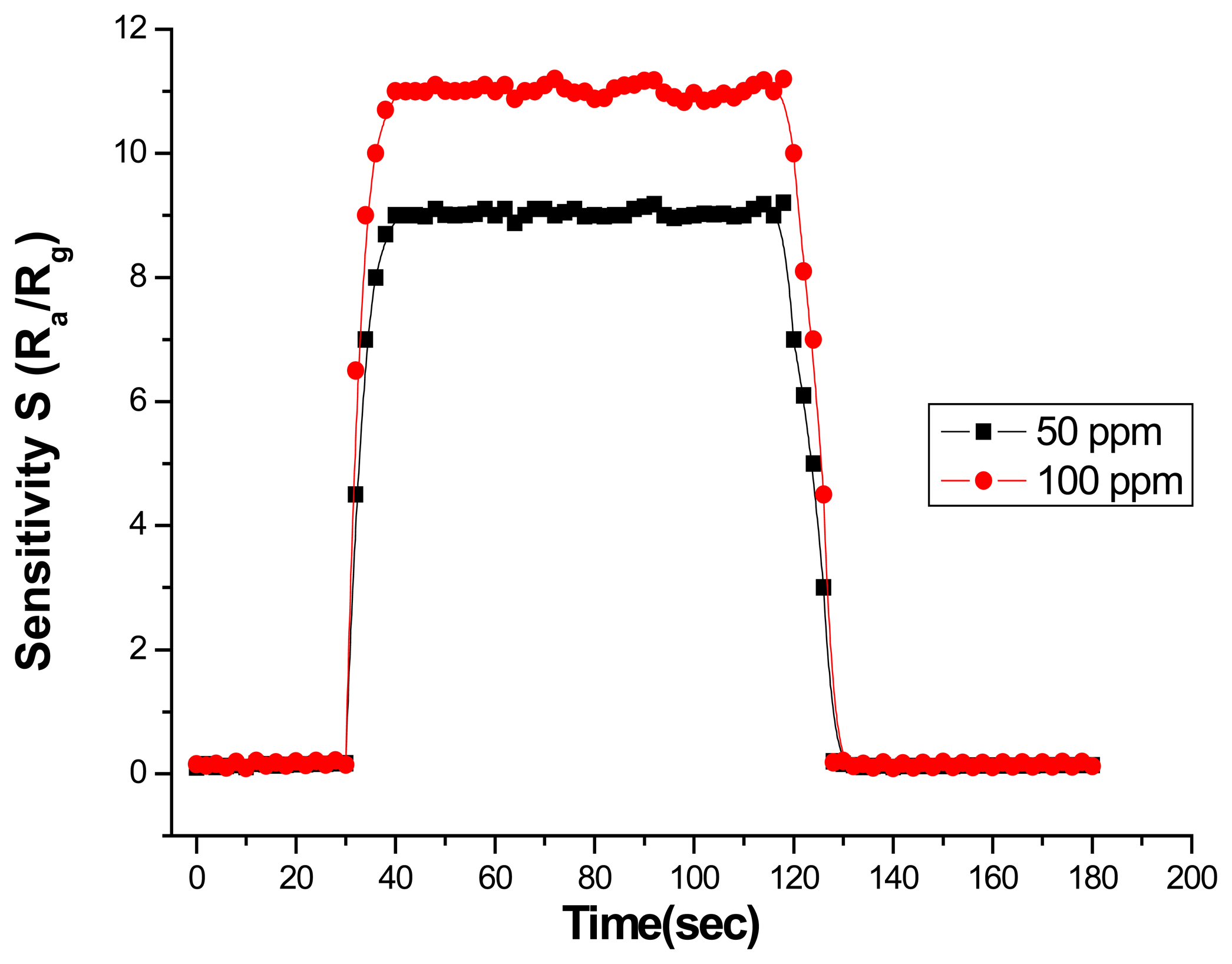
Gas sensing property

In the beginning, pure CO gas was passed through the test chamber to remove any residual gas or water vapors. Then fresh air was passed and maintained till constant sensor resistance was obtained as Ra. The test gas was then admitted along with air and Rg was measured, till a constant value of Rg was obtained. Again fresh air was blown through the test chamber until initial Ra value was obtained. The resistances of the fabricated film in air (Ra) and in the CO gas containing environment (Rg) were used to calculate the sensitivity of the sensor as S = Ra/Rg.
Different compositions of the nanomaterials were synthesized to determine the catalytic ability of the PdOx additives for high sensitivity to CO. As shown in Figure 6 the best composition for the sensor material that gave maximum sensitivity for CO was in the ratio of 5 wt% In2O3/ SnO2:PdOx as 99:1(wt%). In the subsequent studies this weight% ratio of this composite was maintained. The 5 wt% In2O3/ SnO2:PdOx nanocrystalline film also showed higher sensitivity value (9.1) to low level (50 ppm) CO gas at working temperature 200 °C (Figure 6). The sensor has shown good adsorption and desorption for the CO gas at this working temperature.
The response transients of sensors to 50 ppm and 100 ppm CO gas are shown in Figure 7. The response times and the recovery times were very short at about 8 s and 10 s respectively. In addition, the sensitivities of the sensor improve with the increase of CO gas concentration from 50 ppm to 100 ppm.
From the results of gas sensing property, it is clear that the addition of the noble metal not only increases the sensitivity, but also lowers the maximum sensitivity temperature. The basic concepts for increasing the sensitivity and selectivity of the semiconductor materials by adding the noble metals have also been discussed by Shimizu and Egashira [20]. In the present case, we may conclude the enhancement of sensitivity due to the following facts:
The application of nano-scaled SnO2 or In2O3/ SnO2 particles enables exposure of the gas to the maximum surface area.
The compatibility of noble metal salt with the surfactant may result in a well-dispersed distribution of nano sized catalyst particles over the sensing films.

Conclusion

SnO2 and In2O3/ SnO2 nanocrystalline powders were prepared by the sol-precipitate method and heat-treatment. The nanocrystalline powders were proved to be of rutile structure. The samples with smaller particle size make XRD pattern broader because of the small size effect of nanoctystalline. From DTA results, it is shown that the nanocrystalline powders are formed from the SnO3H2 colloidal precipitate through dehydration at different temperatures.
A high-performance CO sensor based on a simple device utilizing SnO2 or In2O3/ SnO2 nanocrystalline material with PdOx was fabricated and demonstrated. The CO sensing characteristics including CO detection sensitivity and transient responses of the sensor device under different CO concentrations were measured and investigated. The sensor based on of 5 wt% In2O3/ SnO2 (1 wt% PdOx) nanocrystalline film prepared by sol-precipitate method has shown high response and good sensitivity to CO at low temperature (200 °C). The response time is about 8 s and recovery time is shorter than 10 s in presence of 50 ppm CO gas. This sensor can be a promising practical device for the low concentration CO gas detection. In the future, we shall report the selectivity and long-term stability test of In2O3/ SnO2 system micro gas sensors.

Acknowledgments

This Research was performed for the Hydrogen Energy R&D Center, one of the 21st Century Frontier R&D Program, funded by the Ministry of Science and Technology of Korea.

References

  1. Birringer, R. Nanocrystalline materials. Mater. Sci. Eng. A 1989, 117, 33–43. [Google Scholar]
  2. Glieter, H. Nanostructured materials. Adv. Mater. 1992, 4, 474–481. [Google Scholar]
  3. Han, S.D.; Huang, S.Y.; Campet, G.; Kennard, M.A. Influence of the pH values of the sol-gel state on the properties of SnO2 nanocrystalline powders obtained from a sol-gel route. Active Passive Elec. Comp. 1995, 18, 53–60. [Google Scholar]
  4. Dawar, A.L.; Joshi, J.C. Review semiconducting transparent tin films: their properties and applications. J. Appl. Phys. 1980, 59, 6243–6251. [Google Scholar]
  5. Zhang, D.Y.; Wang, D.Z.; Wu, Y.H.; Wang, A. Investigation of nanocrystalline SnO2. Mater. Sci. Eng. B 1991, 8, 189–192. [Google Scholar]
  6. Ihokura, K.; Watson, J. The Stannic Oxide Gas Sensor; CRC Press: Boca Raton, 1994; ISBN 0-8493 2604-4. [Google Scholar]
  7. Heilig, A.; Barsan, N.; Weimer, U.; Schweizer-Berberich, M.; Gardner, J.W.; Göpel, W. Gas identification by modulating temperatures of SnO2-based thick-film sensors. Sensors and Actuators B 1997, 43, 45–51. [Google Scholar]
  8. Heilig, A.; Barsan, N.; Weimar, U.; Göpel, W. Selectivity enhancement of SnO2 gas sensors: Simultaneous monitoring of resistances and temperatures. Sens. Actuators B 1999, 58, 302–309. [Google Scholar]
  9. Barsan, N.; Stettner, J.R.; Findley, M.; Göpel, W. High performance gas sensing of CO: Comparative tests for (SnO2-based) semiconducting and for electrochemical sensors. Sensors and Actuators B 2000, 66, 31–33. [Google Scholar]
  10. Shimizu, Y.; Kai, S.; Takao, Y.; Hyodo, T.; Egashira, M. Correlation between methylmercaptan gas-sensing properties and its surface chemistry of SnO2-based sensor materials. Sensors and Actuators B 2000, 65, 349–357. [Google Scholar]
  11. Becker, T.; Ahlers, S.; Braunmuhl, C.B.; Muller, G.; Kiesewetter, O. Gas sensing properties of thin and thick film tin oxide materials. Sensors and Actuators. B 2001, 77, 55–61. [Google Scholar]
  12. Starke, T.K.H.; Coles, G.S.V. Laser-ablated nano-crystalline SnO2 material for low-level CO detection. Sensors and Actuators B 2003, 88, 227–233. [Google Scholar]
  13. Mandayo, G.G.; Castano, E.; Gracia, F.J.; Cirera, A.; Cornet, A.; Morante, J.R. Strategies to enhance the carbon monoxide sensitivity of tin oxide thin film. Sensors and Actuators B 2003, 95, 90–96. [Google Scholar]
  14. Sako, T.; Ohmi, A.; Yumoto, H.; Nishiyama, K. ITO-film gas sensor for measuring photodecomposition of NO2gas. Surface and Coatings Technology 2001, 142-144, 781–785. [Google Scholar]
  15. Patel, N.G.; Patel, P.D.; Vaishnav, V.S. Indium tin oxide (ITO) thin film gas sensor for detection of methanol at room temperature. Sensors and Actuators B 2003, 96, 180–189. [Google Scholar]
  16. Wang, Y.; Wu, X.; Li, Y.; Zhou, Z. Meso-structural SnO2 as sensing material for gas sensors. Solid State Elect. 2004, 48, 627–632. [Google Scholar]
  17. Seal, S.; Shukla, S. Nanocrystalline SnO2 gas sensor in view of the surface reactions and modifications. JOM 2002, 54, 35–38. [Google Scholar]
  18. Shukla, S.; Patil, S.; Kuiry, S.C.; Rahman, Z.; Du, T.; Ludwig, L.; Parish, C.; Seal, S. Synthesis and characterization of sol-gel derived nanocrystalline tin oxide thin film as hydrogen sensor. Sensors and Actuators B 2003, 96, 343–353. [Google Scholar]
  19. Schweizer-Berberich, M.; Strathmann, S.; Weimar, U.; Sharma, R.; Seube, A.; Peyre-Lavigne, A.; Gopel, W. Strategies to avoid VOC cross-sensitivity of SnO2-based CO sensors. Sensors and Actuators B 1999, 58, 318–324. [Google Scholar]
  20. Shimizu, Y.; Egashira, M. Basic concepts and challenges of semiconductor gas sensors. MRS Bulletin 1999, 24, 18–24. [Google Scholar]
Figure 1. Preparation process of In2O3/ SnO2 nanocrystallites.
Sensors 06 00526f1
Figure 2. SEM photography of completed sensor substrate using the MEMS process.
Sensors 06 00526f2
Figure 3. The DTA profiles of SnO2 (A), 5 wt.% In2O3/ SnO2 (B) and 10 wt.% In2O3/ SnO2 (C) precursors.
Sensors 06 00526f3
Figure 4. TEM micrographs of SnO2 (A), 5 wt.% In2O3/ SnO2 (B) and 10 wt.% In2O3/ SnO2 (C), calcined at 800 °C for 2 h.
Sensors 06 00526f4
Figure 5. XRD patterns of SnO2 (A), 5 wt.% In2O3/ SnO2 (B) and 10 wt.% In2O3/ SnO2 (C) nanocrystalline powders, calcined for 2 h at (b) 800 °C, (c) 600 °C, (d) 500 °C, (e) 400 °C, (f) 300 °C and (g) 200 °C.
Sensors 06 00526f5
Figure 6. Sensitivity of the sensor films with different composition in accordance against CO gas at the working temperature 200 °C.
Sensors 06 00526f6
Figure 7. The response transients of sensors to 50 ppm and 100 ppm CO gas at the working temperature 200 °C.
Sensors 06 00526f7
Table 1. The effect of the particle size of the sample with different doped quantities on the calcining temperature.
No.abcdefg
T(°C)80200300400500600800
SnO22.93.13.85.37.813.224.5
D(nm)
5% In-SnO2
3.13.54.56.47.910.5
D(nm)
10% In-SnO2
3.13.75.76.68.7
D(nm)

