Biasing Voltage Dependence of Sensitivity of Electron Beam Evaporated SnO2 Thin Film CO Sensor

Physics Department, King Fahd University of Petroleum and Minerals, Dhahran 31261, Saudi Arabia.
Sensors 2006, 6(9), 1153-1160; https://doi.org/10.3390/s6091153
Submission received: 15 March 2006
/
Accepted: 28 July 2006
/
Published: 26 September 2006
(This article belongs to the Special Issue Gas Sensors)
Abstract
:Thin films of tin oxide were deposited by electron beam evaporation. The effects of the sensor biasing voltage and film thickness on the CO-sensing of tin oxide thin films were investigated. The films were characterized using X-ray diffraction and X-ray photoelectron spectroscopy All the films were found to be amorphous. The current-voltage characteristic of the sensor in air has shown that semiconductor-metal interface forms Schottky barrier. It was found that the CO-sensing properties depend on the sensor biasing voltage and film thickness. For lower biasing voltages the sensitivity was much higher than for the higher voltages. It was found that the sensitivity of the films to CO increased with the film thickness.
1. Introduction
Tin oxide based semiconductor gas sensors have been widely used for detection of the environmentally hazardous pollutant gases in general and carbon monoxide gas in particular [1,2,3,4,5,6]. However their detecting mechanism is not fully yet established. Film parameters that are widely known to affect the sensing properties of a thin film are surface roughness, stoichiometry, grain size, structure (amorphous or polycrystalline), and porosity [1,2,3,4,5,6]. Furthermore depending on the preparation conditions of the sensing layers (physical vapor deposition, chemical vapor deposition, screen-printed and sintered materials) and also on the sensor design (nature and geometry of the electrodes), large differences of behavior concerning gas response and selectivity are observed [7,8,9]. For screen printed thick film tin oxide CO sensor it has been reported that the electrode materials of silver and gold influences the detection property [8,9]. More recently while studying the effects of the electrode metals and configuration on the CO sensing of tin oxide thin films it was found that the CO-sensing properties depend both on the electrode metals and configuration [10]. Moreover while studying the effects of the film thickness and preparation conditions (films prepared with or without the presence of oxygen environment during deposition) on the optical and carbon monoxide sensing properties of the films it was shown that the CO-sensing properties strongly depend on the film thickness and preparation conditions [1]. Although various parameters of SnO2 thin film CO sensor has been studied thoroughly in the past, however nothing or very little has been published on the dependence of electron beam evaporated thin film SnO2 CO sensor on the sensor biasing voltages. Therefore, the aim of the present work was to study the dependence of thin film SnO2 CO sensor sensitivity on the sensor biasing voltages.
2. Experimental Details
Thin films of tin oxide having thicknesses ranged from about 200 to 400 nm were prepared in a Leybold L560 box coater pumped by a turbomolecular pump. The system was pumped to a base pressure of 4 x 10⁻⁶ mbar. The films were deposited by electron beam evaporation under the oxygen partial pressure of 5 x 10⁻⁴ mbar. Before deposition, the material was slowly outgassed with a shutter blocking the vapor from the sample surface. For different purposes of film characterization (XPS, XRD), the films were simultaneously deposited on different substrates: BK7 glass and tantalum substrates. The substrates were rotated during the deposition. A constant rate of evaporation of 0.4 nm/s was controlled by a quartz crystal thickness monitor and rate controller. The source-to-substrate distance was about 45 cm. In the preparation of the films, oxygen was readmitted to raise the pressure of the coating chamber to 5 x 10⁻⁴ mbar. After the films were deposited, they were removed from the coating chamber, and a variety of characterization techniques were employed to study their various properties. The chemical composition of the films was studied using X-ray photoelectron spectroscopy (XPS), and was performed in a VG Scientific ESCALAB MKII spectrometer using Al Kα (1486.6 eV) radiation. The instrumental resolution was 1.2 eV with a slit width of 6 mm. Samples were maintained at ambient temperature at a pressure of 5 x 10⁻⁹ mbar. The films deposited on tantalum substrates were used for the XPS analysis, so that charging of nonconducting samples could be reduced. Film structure was examined by X-ray diffraction (XRD), and was performed in a JEOL JDX-3530 X-ray diffractometer using Cu Kα radiation (1.54 Å). The films deposited on BK7 glass were used for the XRD analysis. The 2θ range studied was 0-80o. The 2θ step and step acquisition time were 0.02o and 1.00 s, respectively.
The resistances of the films were determined from the measurement of the current passing through the sample at different bias voltages. The measurements were done in air and air-CO mixture, in the temperature range 25-500 oC. The thicknesses of the films ranged from about 200 to 400 nm. Prior to the deposition of the films, gold electrodes of length 7 mm and electrode spacing of 2 mm were deposited on glass substrates by thermal evaporation. Platinum lead wires were then attached onto contact pads of the electrodes with an electrically conducting paste (Aremco-Bond 597/C). Before starting with the measurements the films were thermally annealed at a temperature of 400 0C for 4 hours under atmospheric conditions with the aim to stabilize their physical parameters.
3. Results and Discussion
3.1 Characterization of films
The X-ray diffraction patterns obtained for all the films showed a broad peak, which is typical of an amorphous structure. Annealing of the films in air at a temperature of 400 0C had no effect on the nature of the diffraction patterns.
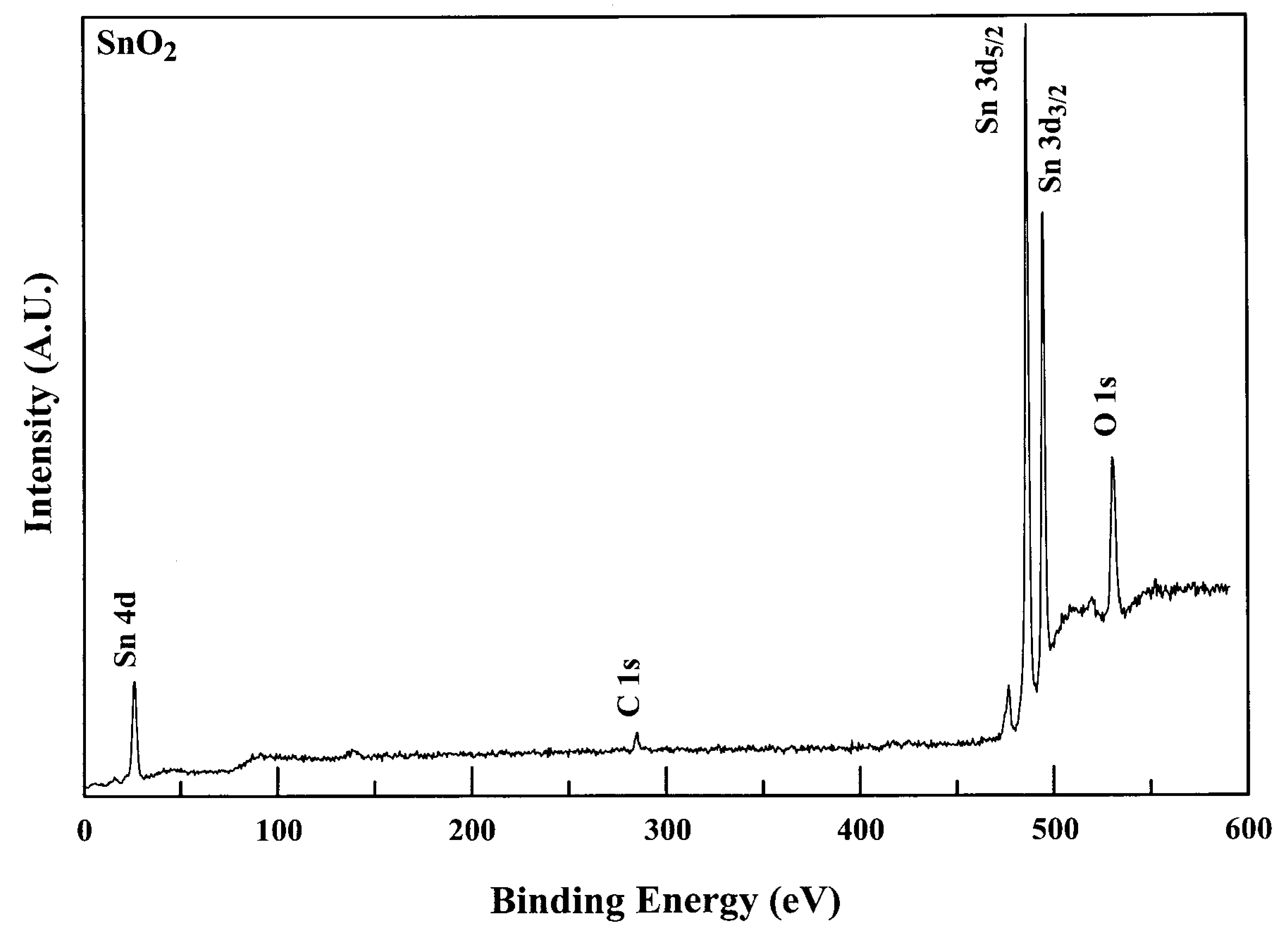
Figure 1 shows an XPS wide scan spectrum of a tin oxide film. The scan shows sharp lines due to the main constituents (Sn and O) and the carbon C 1s peak arising from hydrocarbon contamination. The C 1s peak, at a binding energy (BE) of 284.6 eV, was used to make corrections for charge shift. The atomic ratio of oxygen to tin (O/Sn) was determined from the areas of the O 1s and Sn 3d3/2 peaks. The values of the ratio were found to be: 2.18 (as-deposited) and 1.85 (annealed in air at a temperature of 400 0C).
Figure 1.
A wide scan x-ray photoelectron spectrum of tin oxide film.

For the as-deposited films, the atomic ratio was higher than the stoichiometric value of 2. This hyper-stoichiometry may be due to the presence of tin hydroxide and/or trapped oxygen in the films [11,12]. XPS is a surface technique that probes only a few top monolayers, and thus, cannot reveal the O/Sn ratio in the bulk of the film. Nevertheless, the O/Sn ratio showed the expected trend, i.e. it increased with the introduction of oxygen and decreased upon annealing the films in air. The uncertainty in the measurement of the atomic ratio O/Sn was about 10%.
3.2 CO gas-sensing properties
The CO gas-sensing properties of the oxide films were studied by measuring the film resistance in air (Rair) and in presence of dry air containing different concentrations of CO (RCO). The CO gas showed a reducing effect, leading to a decrease in the electrical resistance as in most of the n-type metal oxide semiconductors [6]. For reducing gases the sensitivity S is defined as ΔR/Rair where ΔR=Rair-RCO. The sensitivity was measured as a function of sensor temperature and sensor biasing voltages. The sensor was placed in a direct contact with a heated copper disc. The heating of the disc was provided by nichrome wire (covered by alumina tubes) heater passing through the disc. The temperature of the sensor was controlled by varying the magnitude of the applied voltage to the heating element. It was found that the Sensitivity (S) measured at a given temperature, in addition to other film preparation conditions (films prepared with or without the presence of oxygen environment during deposition, film thickness, porosity, electrode metals and configuration [1,10]) also strongly depends on the sensor biasing voltage. Before starting with the measurements the films were thermally annealed at a temperature of 400 0C for 4 hours under atmospheric conditions with the aim to stabilize their physical parameters.
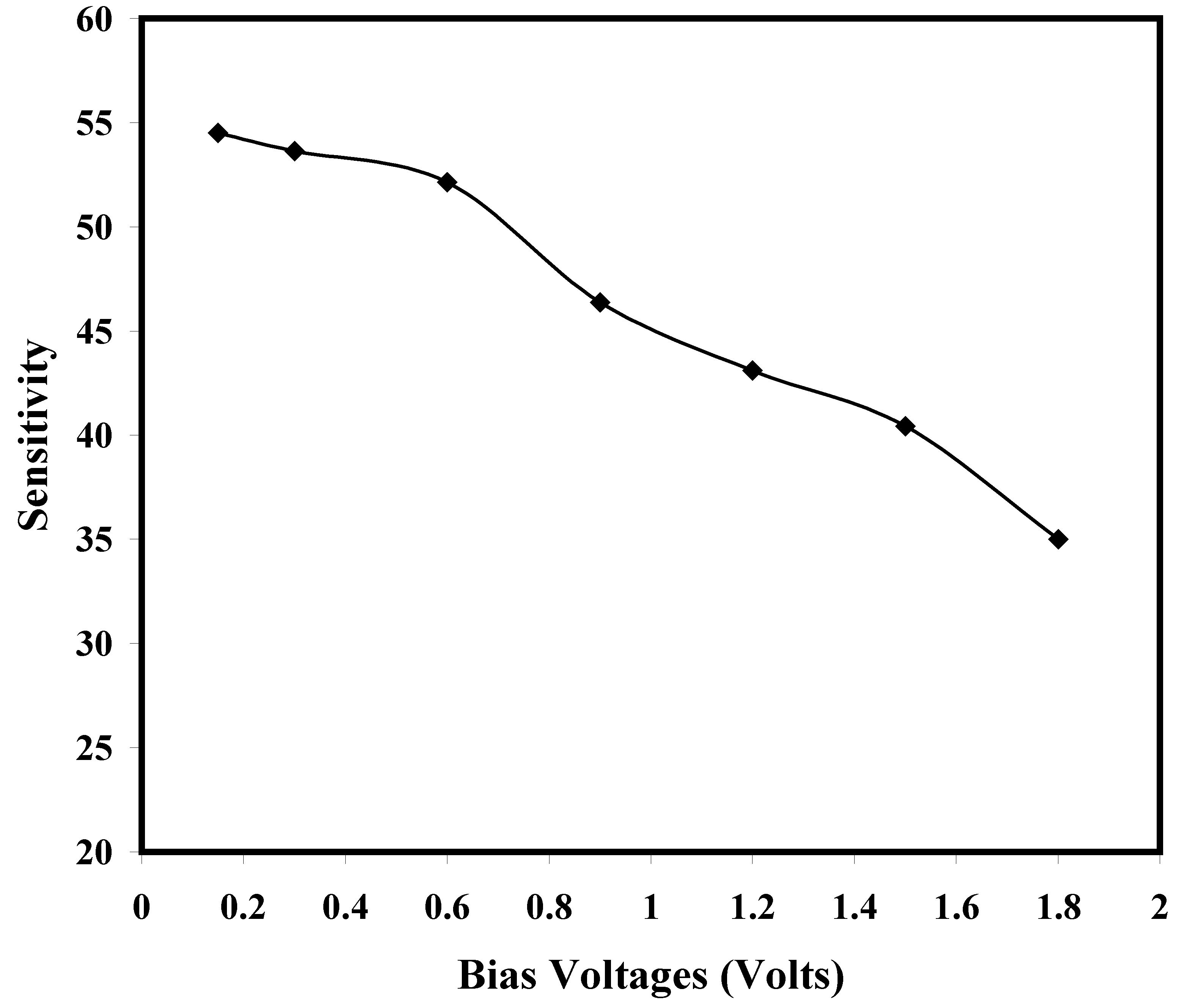
Figure 2.
Sensitivity as a function of biasing voltage for SnO2 sensor of thickness 200 nm, CO concentration of 1000 ppm and temperature of 350 oC.
Figure 2.
Sensitivity as a function of biasing voltage for SnO2 sensor of thickness 200 nm, CO concentration of 1000 ppm and temperature of 350 oC.

Figure 2 shows sensitivity dependence on the sensor bias voltage for SnO2 sensor of thickness 200 nm with CO concentration of 1000 ppm at temperature of 350 oC (optimum operating temperature of SnO2 CO sensor [1, 10]). Figure 2 depicts that there is a significant decrease in sensitivity as the biasing voltages is increased. For the lower biasing voltages the sensitivity is almost 50 percent higher than that of higher biasing voltages. Similar results were observed for other film thicknesses of 180 nm, 300 nm and 400 nm and temperatures of 300 oC and 500 oC.
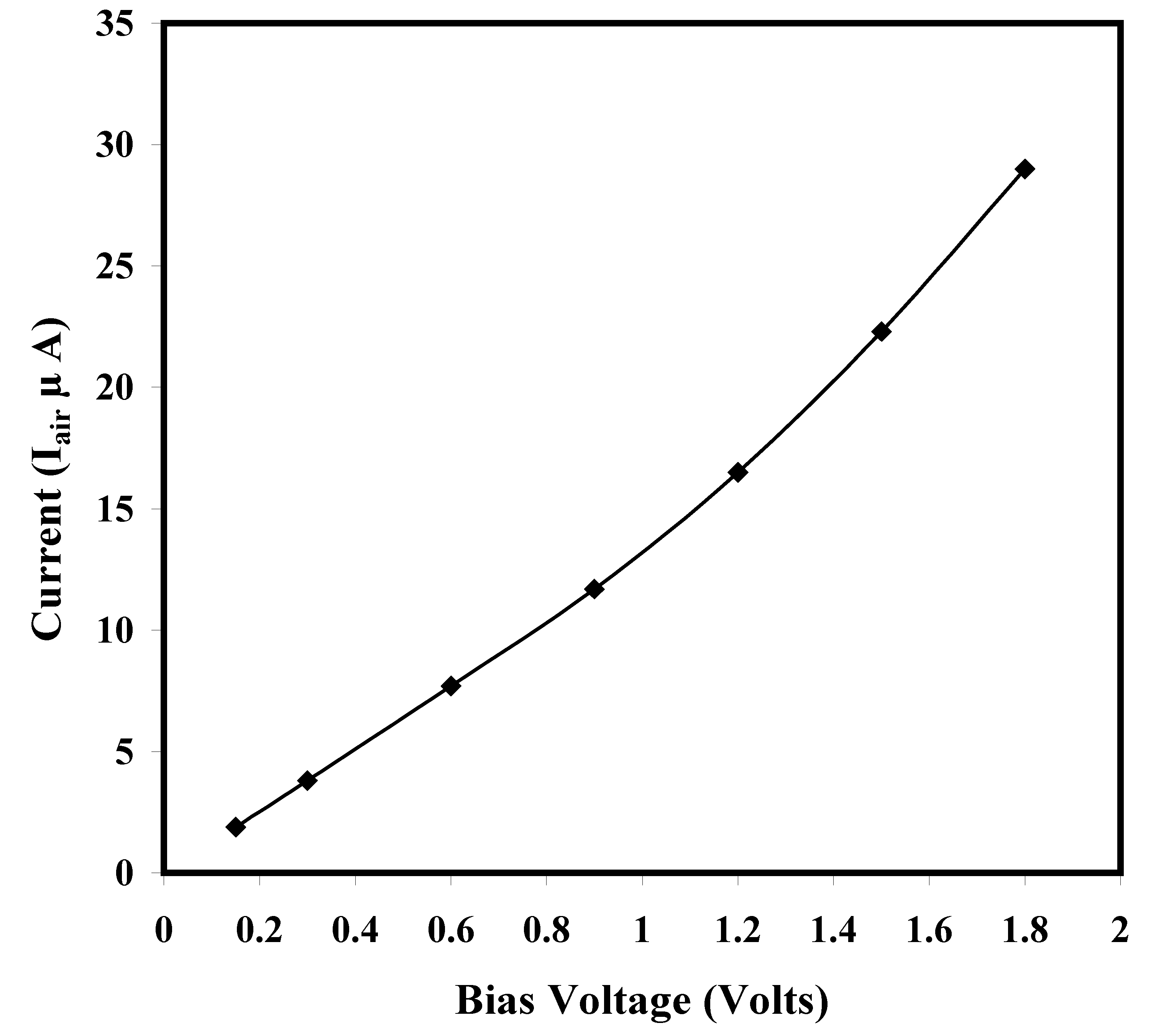
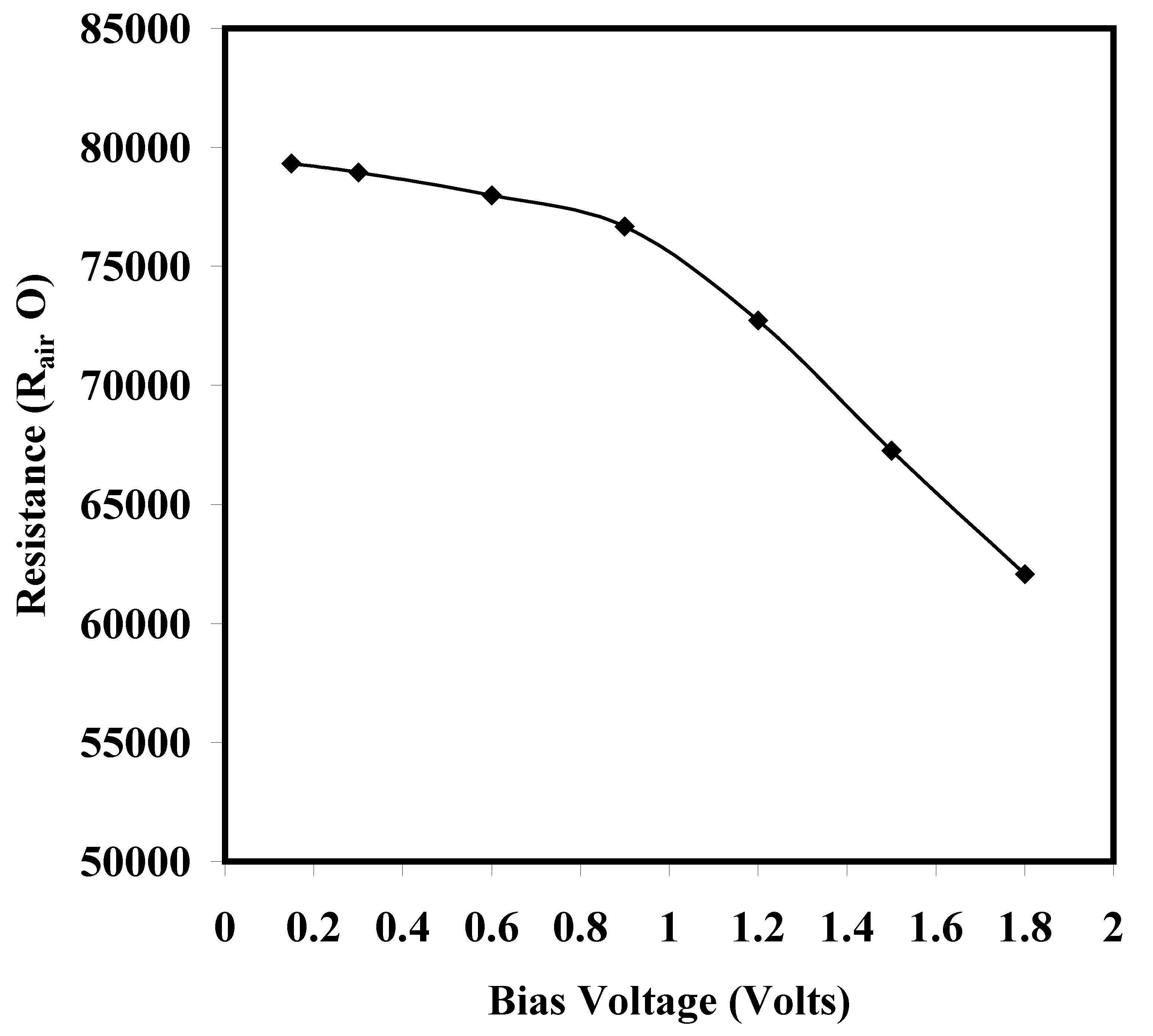
Figure 3 shows current voltage characteristics of SnO2 film of thickness 200 nm in air at 350 oC. It is clear from the Figure that the current-voltage relationship is non-linear (non-Ohmic). Similar non Ohmic trend was observed when a resistance-voltage characteristic was studied for SnO2 film of 200 nm thickness and at the temperature of 350 oC. The non-linearity of the current-voltage-resistance characteristics in Figure 3 and Figure 4 clearly show that the semiconductor-metal interface forms Schottky barrier.
It is known that thick films gas sensor while sensing CO, utilizes the presence of the Schottky barrier. First oxygen from the ambient is adsorbed on the exposed surface of the sensor, extracts electron from the material to form O-. When the sensor is exposed to a reducing gas like CO, the adsorbed CO reacts with the adsorbed O- and releases the trapped electron back to the conduction band, and thereby lowering the barriers height and resistance.
Figure 3.
Current voltage characteristics of SnO2 sensor in air at 350 oC for film thickness of 200 nm.
Figure 3.
Current voltage characteristics of SnO2 sensor in air at 350 oC for film thickness of 200 nm.

Figure 4.
Variation of SnO2 sensor resistance in air with bias voltages at 350 oCfor film thickness of 200 nm.
Figure 4.
Variation of SnO2 sensor resistance in air with bias voltages at 350 oCfor film thickness of 200 nm.
This Schottky barrier controlled conduction mechanism [15,16] is applied for thick film SnO2 and TiO2 based CO sensors for temperatures of approximately 500 oC. In the present case also, Schottky barrier controlled conduction mechanism could be attributed to the sensing behavior of SnO2 thin film sensor. Moreover, the change in the sensitivity with biasing voltage could be attributed to the influence of applied voltage in altering Schottky barrier.
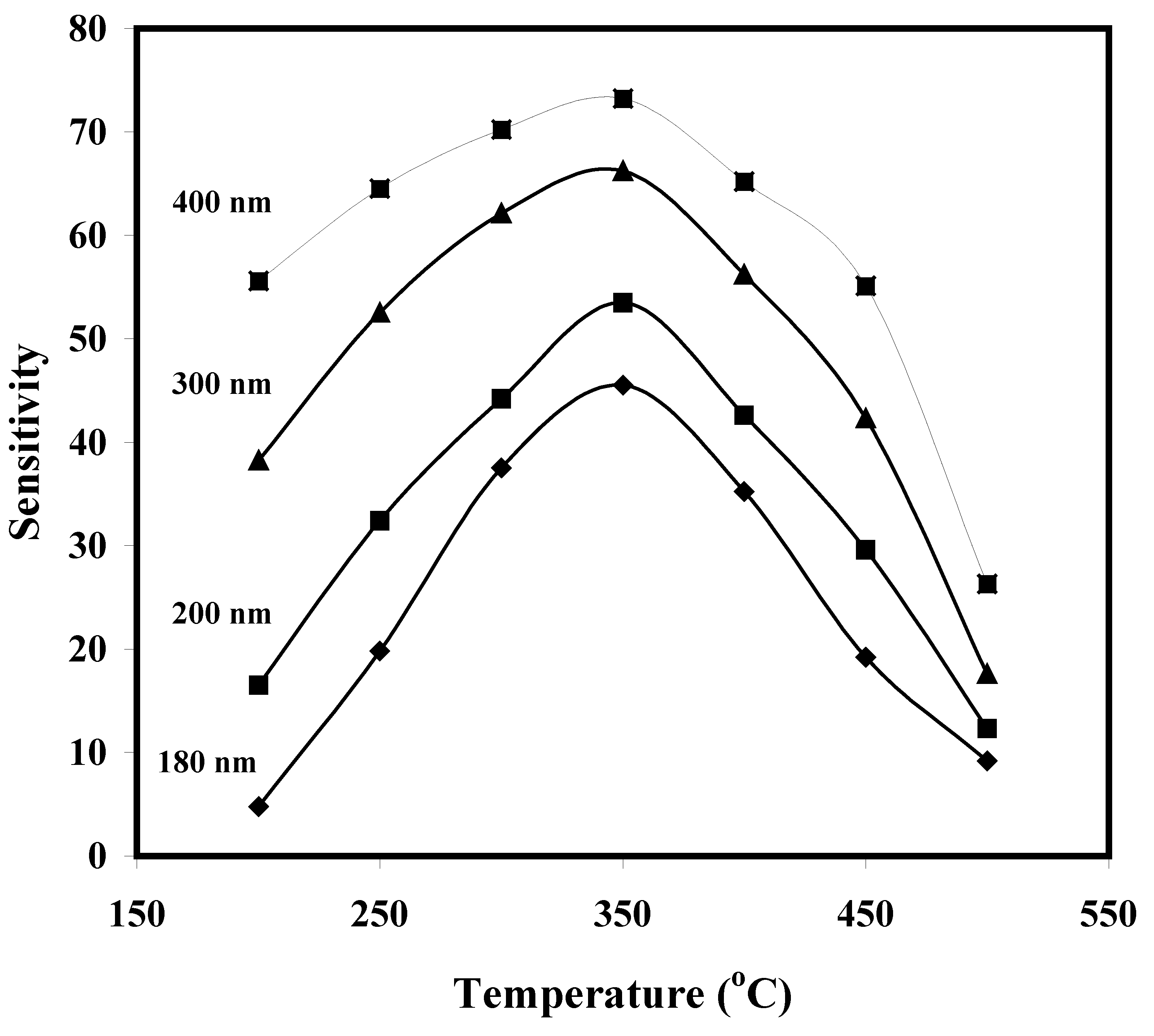
Figure 5 shows the sensitivity as a function of operating temperature for the tin oxide films of different thickness. It was found that at a given operating temperature the sensitivity of the film increased with its thickness.
Increase in sensitivity of thin tin oxide films with thickness, for the CO detection has been recently reported [1]. Increase in the sensitivity for CO with thickness has been observed in thin films of HfO2 [13]. Moreover, this observation may also find a support from a recent work of Becker et al [14] where they studied gas-sensing properties of thin (thickness 50 – 300 nm) and thick (15000 – 80000 nm) films of tin oxide. They concluded that thin films mainly respond to oxidizing gases such as O3 and NO2, whereas thick films preferably respond to reducing species like CO and CH4.
Conclusions
The effects of the biasing voltages on the CO sensing of tin oxide thin films were investigated. The current-voltage-resistance characteristic of the sensor in air has shown the formation of Schottky barrier at semiconductor-metal interface. It was found that the CO-sensing properties depend strongly on the sensor biasing voltages. For lower biasing voltages the sensitivities were much higher (almost 50%) than the higher biasing voltages. The sensitivity of the films increases with thickness of the film.
Figure 5.
Effects of film thickness of a SnO2 sensor on its sensitivity. The COconcentration was 1000 ppm and basing voltage was 0.2 volts.
Figure 5.
Effects of film thickness of a SnO2 sensor on its sensitivity. The COconcentration was 1000 ppm and basing voltage was 0.2 volts.

Acknowledgments
The support provided by the Physics Department of King Fahd University of Petroleum and Minerals is acknowledged. This work is part of project # FT-2001/8. Several useful discussions with Professors S. A. Akbar, E. E. Khawaja, Dr. M. F. Al-Kuhaili and Mr. M. A. Dastageer are appreciated. The assistance of Mr. S. Jaroudi with the XRD measurements and Dr N. Tabet with the XPS measurements is also acknowledged.
References
- Durrani, S. M. A.; Al-Kuhaili, M. F.; Khawaja, E. E. CO-sensing properties of undoped and doped tin oxide thin films prepared by electron beam evaporation. Talanta 2005, 65, 1162–1167. [Google Scholar] [CrossRef] [PubMed]
- Wurzinger, O.; Reinhardt, G. CO-sensing properties of doped SnO2 sensors in H2-rich gases. Sensors and Actuators 2004, B103, 104–110. [Google Scholar] [CrossRef]
- Mandayo, G. G.; Castano, E.; Gracia, F.J.; Cirera, A.; Cornet, A.; Morante, J.R. Strategies to enhance the carbon monoxide sensitivity of tin oxide thin films. Sensors and Actuators 2003, B95, 90–96. [Google Scholar] [CrossRef]
- Matko, I.; Gaidi, M.; Hazemann, J. L.; Chenevier, B.; Labeau, M. Electrical properties under polluting gas (CO) of Pt- and Pd-doped polycrystalline SnO2 thin films: analysis of the metal aggregate size effect. Sensors and Actuators 1999, B59, 210–115. [Google Scholar] [CrossRef]
- Sharma, R. K.; Chan, P. C. H.; Tang, Z.; Yan, G.; Hsing, I. M.; Sin, J. K. O. Sensitive, selective and stable tin dioxide thin-films for carbon monoxide and hydrogen sensing in integrated gas sensor array applications. Sensors and Actuators 2001, B72, 160–166. [Google Scholar] [CrossRef]
- Becker, Th.; Ahlers, S.; Bosch-v. Braünmuhl, Chr.; Müller, G.; Kiesewetter, O. Gas sensing properties of thin- and thick-film tin-oxide materials. Sensors and Actuators 2001, B77, 55–61. [Google Scholar] [CrossRef]
- Montmeat, P.; Marchand, J-C; Lalauze, R.; Viricelle, J-P; Tournier, G.; Pijolat, C. Physico-chemical contribution of gold metallic particles to the action of oxygen on tin dioxide sensors. Sensors and Actuators 2003, B95, 83–89. [Google Scholar] [CrossRef]
- Mishra, V. N.; Agarwal, R. P. Effect of electrode material on sensor response. Sensors and Actuators 1994, B22, 121–125. [Google Scholar] [CrossRef]
- P. Dutronc, B.; Carbonne, F.; Menil, C. Lucat, Influence of the nature of the screen-printed electrode metal on the transport and detection properties of thick-film semiconductor gas sensors. Sensors and Actuators 1992, B 6, 279–284. [Google Scholar] [CrossRef]
- Durrani, S. M. A. The influence of electrode metals and its configuration on the sensitivity of tin oxide thin film CO sensor. Talanta 2006, 68, 1732–1735. [Google Scholar] [CrossRef] [PubMed]
- Khawaja, E. E.; Bouamrane, F.; Hallak, A. B.; Daous, M. A.; Salim, M. A. Observation of oxygen enrichment in zirconium oxide films. J. Vac. Sci. Tech. 1993, A11, 580–587. [Google Scholar] [CrossRef]
- Vink, T. J.; Verbeek, G. F. A.; Snijders, J. H. M.; Tamminga, Y. Physically trapped oxygen in sputter-deposited MoO3 films. J. Appl. Phys. 2000, 87, 7252–7254. [Google Scholar] [CrossRef]
- Al-Kuhaili, M. F.; Durrani, S. M. A.; Khawaja, E. E. Optical Properties of Hafnium Oxide Films Prepared by Electron Beam Evaporation. J. Phys. D: Appl. Phys. 2004, 37, 1254–1261. [Google Scholar] [CrossRef]
- Becker, Th.; Ahlers, S.; Bosch-v.Braunmühl, Chr.; Müller, G.; Kiesewetter, O. Gas sensing properties of thin- and thick-film tin-oxide materials. Sensors and Actuators 2001, B77, 55–51. [Google Scholar] [CrossRef]
- Akbar, S. A.; Younkman, L. B. Sensing mechanism of a titania-based CO sensor. J. Electrochemical Society 1997, 144, 1750–1753. [Google Scholar] [CrossRef]
- Shimizu, Y.; Nakamura, Y.; Egashira, M. Effect of diffusivity of hydrogen and oxygen through pore of thick film SnO2-based sensor on their sensing properties. Sensors and Actuators 1993, B13, 128–131. [Google Scholar] [CrossRef]
© 2006 by MDPI (http://www.mdpi.org). Reproduction is permitted for noncommercial purposes.
Share and Cite
MDPI and ACS Style
Durrani, S.M.A. Biasing Voltage Dependence of Sensitivity of Electron Beam Evaporated SnO2 Thin Film CO Sensor. Sensors 2006, 6, 1153-1160. https://doi.org/10.3390/s6091153
AMA Style
Durrani SMA. Biasing Voltage Dependence of Sensitivity of Electron Beam Evaporated SnO2 Thin Film CO Sensor. Sensors. 2006; 6(9):1153-1160. https://doi.org/10.3390/s6091153
Chicago/Turabian StyleDurrani, Sardar M. Ayub. 2006. "Biasing Voltage Dependence of Sensitivity of Electron Beam Evaporated SnO2 Thin Film CO Sensor" Sensors 6, no. 9: 1153-1160. https://doi.org/10.3390/s6091153