Modeling and Manufacturing of Micromechanical RF Switch with Inductors

Department of Mechanical Engineering, National Chung Hsing University, 250 Kuo-Kuang Rd., Taichung, 402 Taiwan, R.O.C.
*
Author to whom correspondence should be addressed.
Sensors 2007, 7(11), 2660-2670; https://doi.org/10.3390/s7112670
Submission received: 18 October 2007
/
Accepted: 7 November 2007
/
Published: 9 November 2007
(This article belongs to the Special Issue Modeling, Testing and Reliability Issues in MEMS Engineering)
Abstract
:This study presents the simulation, fabrication and characterization of micromechanical radio frequency (RF) switch with micro inductors. The inductors are employed to enhance the characteristic of the RF switch. An equivalent circuit model is developed to simulate the performance of the RF switch. The behaviors of the micromechanical RF switch are simulated by the finite element method software, CoventorWare. The micromechanical RF switch is fabricated using the complementary metal oxide semiconductor (CMOS) and a post-process. The post-process employs a wet etching to etch the sacrificial layer, and to release the suspended structures of the RF switch. The structure of the RF switch contains a coplanar waveguide (CPW), a suspended membrane, eight springs and two inductors in series. Experimental results reveal that the insertion loss and isolation of the switch are 1.7 dB at 21 GHz and 19 dB at 21 GHz, respectively. The driving voltage of the switch is about 13 V.
1. Introduction
Radio frequency (RF) switches are important components in wireless communication systems [1]. A comparison with solid-state RF switches reveals that the micromechanical RF switches have the advantages of low insertion loss and excellent isolation, and high linearity at microwave and millimeter-wave frequencies [2-3]. Many micromechanical switches have recently been manufactured using microelectromechanical system (MEMS) technology. For instance, Zheng et al. [4] employed a surface micromachining process to fabricate an RF MEMS membrane switch on GaAs substrate. The fabrication of the RF switch consisted of defining the CPW lines of AuGeNi/Au, depositing a dielectric layer of SiN and a sacrificial layer of polyimide, electroplating a membrane of Au and using developer to remove the sacrificial polyimide layer. The actuation voltage of the switch was about 17 V, and the switch had an insertion loss of 0.25 dB at 25.6 GHz and an isolation of 42 dB at 24.5 GHz. A micromachined microwave switch proposed by Chang et al. [5] was made on a semi-insulating GaAs substrate using a surface micromachining process, in which the process included using lift-off technique to pattern the CPW lines of Cr/Au, depositing a dielectric layer of SiO2 and a sacrificial layer of amorphous silicon, defining the actuator structure layers of Al/Cr deposited by electron beam evaporation, and etching the sacrificial amorphous silicon layer to release the actuator structure. The switch had an actuation voltage of 26 V, and the insertion loss and isolation of the switch were 0.2 dB at 10 GHz and 17 dB at 10 GHz. Park et al. [6] manufactured an RF MEMS capacitive switch using a surface micromachining process. The CPW lines of Cr/Au/Pt were formed by lift-off technique, and the dielectric of STO (strontium titanate oxide) was deposited by a RF sputter. Polyimide was adopted as a sacrificial layer, and the structure layer of Au was formed by electroplating technique. Finally, the movable structures were released by etching the sacrificial layer using a barrel plasma etcher. The switch had an isolation of 42 dB at 5 GHz and an insertion loss of 0.08 dB at 10 GHz, and the actuation voltage was 8 V. In this work, we employ the CMOS-MEMS technique to fabricate a micromechanical RF capacitive switch, which the fabrication of the switch is easier than Zheng et al. [4], Chang et al. [5] and Park et al. [6]. The switch requires only one wet etching post-process to release the suspended structures after completion of the CMOS process. The post-process has the benefits of easy execution and low cost.
The technique that utilizes the commercial CMOS process to manufacture MEMS devices is known as CMOS-MEMS [7-8]. The advantage of micromechanical switches fabricated by the CMOS-MEMS technique is the capability for integration with RF circuits in the system-on-a-chip (SOC) application. We had used the CMOS-MEMS technique to develop a micromechanical switch [9] on silicon substrate. In this work, series inductors are integrated with the micromechanical switch [9] for improving its performance. The micromechanical RF switch with inductors is also fabricated using the CMOS-MEMS technique. A wet etching post-CMOS process is used to release the suspended structures of the switch. The switch that is actuated by an electrostatic force is a capacitive shunt type. Experimental results reveal that the actuation voltage of the switch is about 13 V, and the switch has an insertion loss of 1.7 dB at 21 GHz and an isolation of 19 dB at 21 GHz. Finally, in order to investigate the switch more deeply, an equivalent circuit is developed to evaluate the insertion loss and isolation of the switch.
2. Simulation of the RF switch
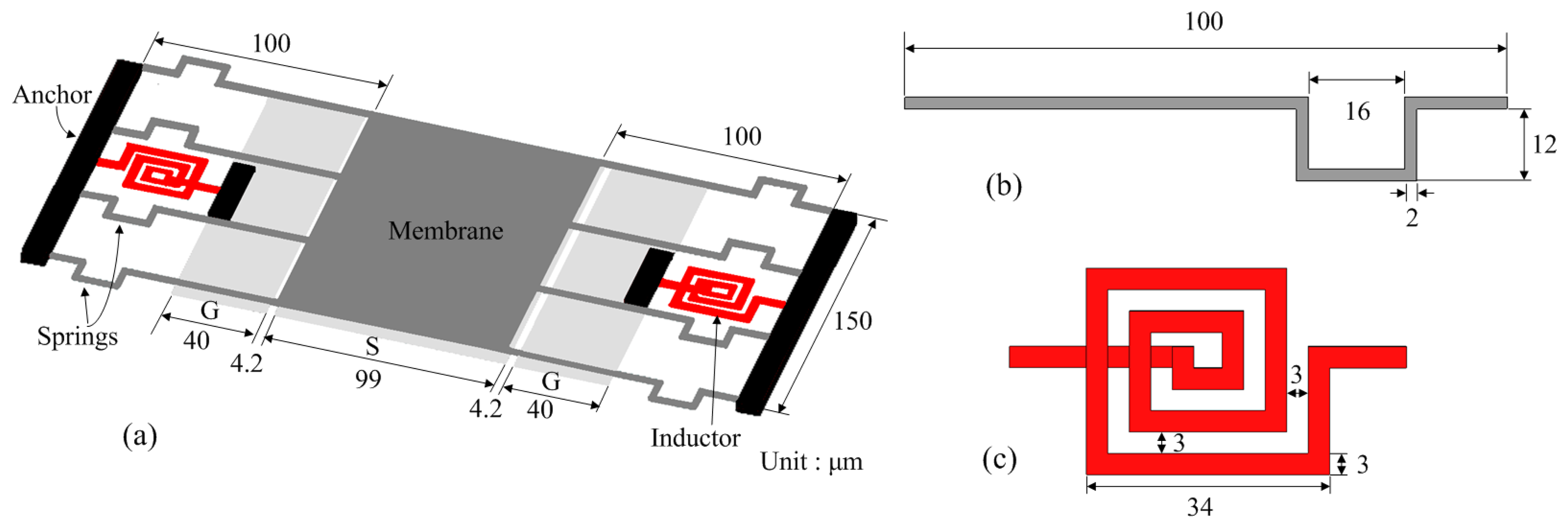
The structure of the micromechanical RF switch is illustrated in Figure 1(a). The micromechanical RF switch consists of a membrane, eight springs, two inductors, anchors and CPW transmission lines. The CPW transmission lines are composed of ground (G), signal (S) and ground (G) lines. The signal line of CPW, which locates under the membrane, is 99 μm wide and about 0.67 μm thick. The ground lines of CPW are 40 μm wide and about 0.67 μm thick. The space between the ground and signal lines is 4.2 μm. The membrane and eight springs are the suspended structures, and the membrane is supported by eight springs. The area of the membrane is 99×150 μm2. The anchors are connected to the ground lines of CPW by the inductors. Figure 1(b) shows the dimensions of a spring that is 100 μm long and 2 μm wide, and all springs have the same dimensions. The thickness of springs and membrane is approximately 1 μm. Figure 1(c) shows the dimensions of an inductor that has 2.5 turns, and the two inductors have the same dimensions. The RF switch, which is actuated by electrostatic force, is a capacitive shunt type. The membrane actuated by the electrostatic force stays in the down position upon applying an actuation voltage. The RF signal propagated in the signal line of CPW is coupled to the ground plane, so the switch is at the ‘off’ state. In contrast, the membrane supported by the springs stays in the up position when there is no applied voltage. The RF signal propagates in the signal line of CPW, so that the switch is at the ‘on’ state.
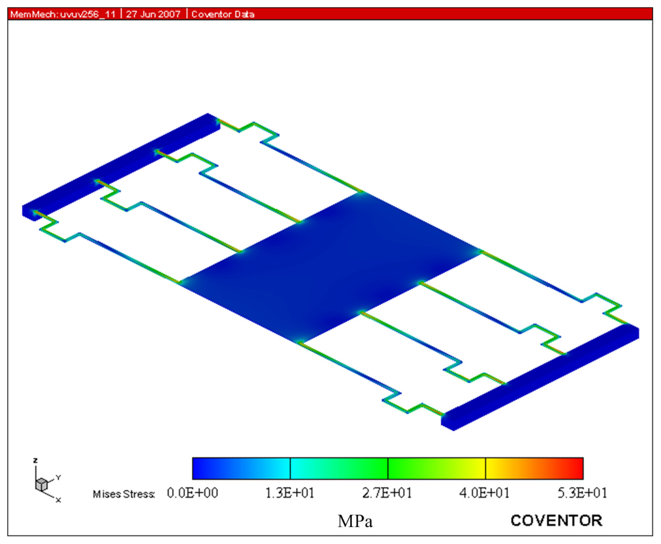
The finite element method software, CoventorWare, is utilized to simulate the behaviors of the micromechanical RF switch. The model of the micromechanical RF switch is established in accordance with the dimensions in Figure 1, and then the model is meshed using triangular elements. The material of the switch is aluminum with a Young's modulus of 70 GPa, Poisson's ratio of 0.3 and mass density of 2679 kg/m3[10]. Finally, the displacement and stress of the switch are evaluated. Figure 2 illustrates the displacement distribution of the switch with a driving voltage of 13 V, in which the membrane exhibits a uniform out-of-plane displacement of 3.3 μm. Figure 3 depicts the relation between the membrane displacement and driving voltage in the switch. The simulated result shows that the switch has a pull-in voltage of about 13 V. Figure 4 shows the stress distribution of the filter when a driving voltage of 13 V is applied. The maximum stress of 53 MPa located at the end of the springs in the switch is below the yield strength of aluminum (124 MPa). Therefore, the motion of the switch can be operated in the elastic range.
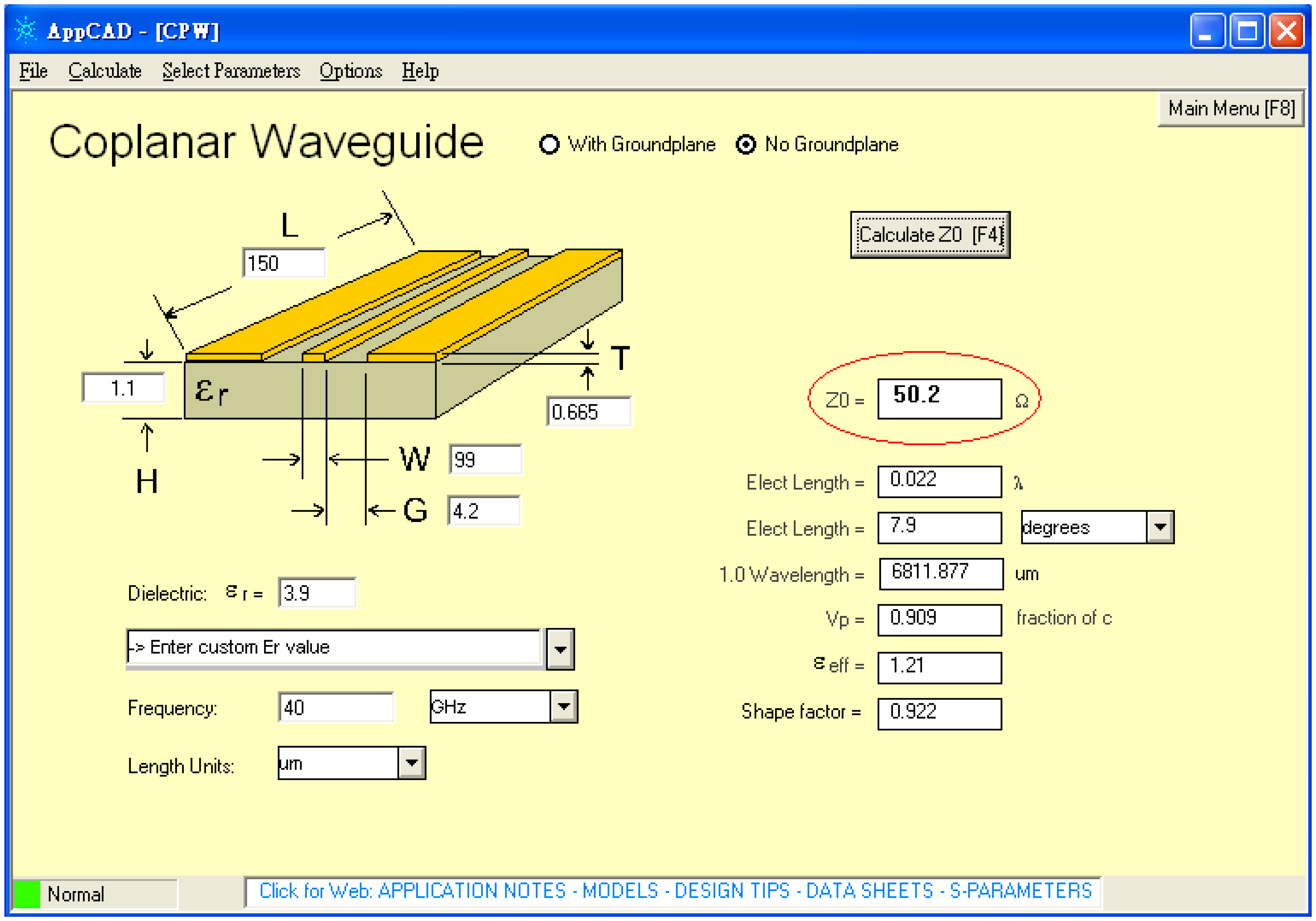
The Agilent CAD tool is used to calculate the characteristic impedance of the CPW. The dimensions of the CPW, as shown in Figure 1(a), are inputted to the Agilent CAD tool, and then the calculation is executed. Figure 5 demonstrates the calculated result of the CPW characteristic impedance. The calculated result shows that this CPW has a characteristic impedance of 50.2 Ω, and the value matches the impedance of 50 Ω in the network analyzer. This shows that the electromagnetic wave incident on this switch has a small return loss.
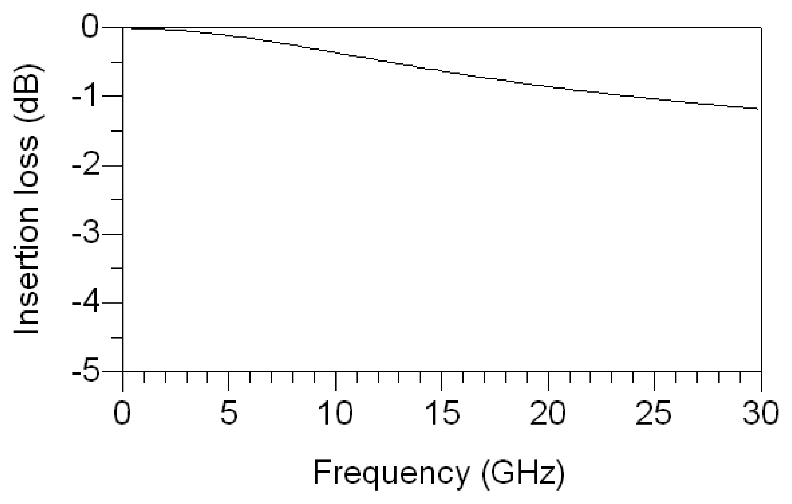
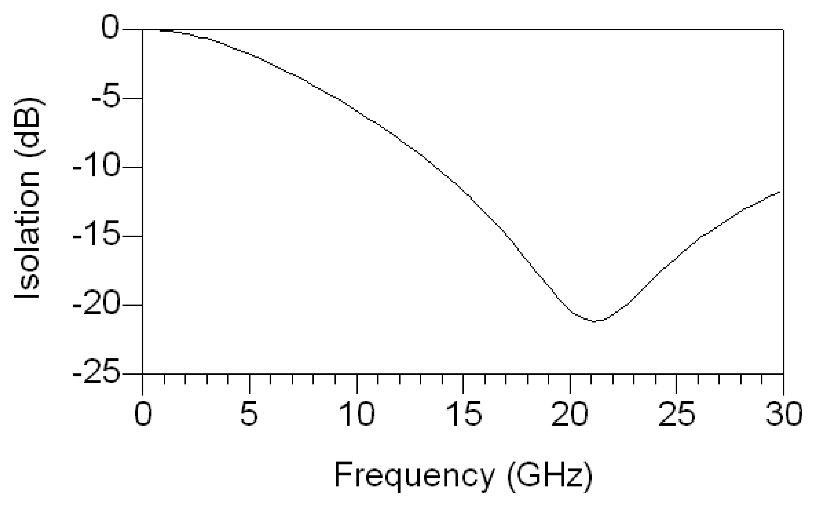
The equivalent circuit of the micromechanical RF switch is shown in Figure 6. The series arm between port-1 and port-2 contains a resistor and an inductor, in which the two components are utilized to describe the signal line behavior. The parallel path at the middle position between ports is composed of Ctune, Lshunt, Rshunt, Lind, Cind and Rind elements, where Ctune is the capacitance between the membrane and the signal line; Lshunt represents the inductance of the membrane and springs; Rshunt is the resistance of the membrane and springs; Lind is the inductance of the series inductors; Cind and Rind are the capacitance and resistance of the series inductors, respectively. The three components of Lind, Cind and Rind are adopted to describe the behavior of series inductors. The parallel path between ports to ground includes Cox, Csub, and Rsub elements. These components represent the silicon substrate loss in the switch. The component of Cox represents the insulator capacitance under the signal line, and the elements of Rsub and Csub are the resistance and capacitance of silicon substrate, respectively. Hence, the capacitance of Ctune is essential in this circuit, and the value of this capacitance expresses the ‘on’ and ‘off’ behaviors of the switch. According to the dimensions of the structure as shown in Figure 1, the parameters of the switch are extracted using the Ansoft Q3D extractor. Table 1 shows the extracted parameters of the switch. The Agilent ADS (advanced design system) is employed to simulate the characteristics of the equivalent circuit (Figure 6) in accordance with the extracted parameters in Tab. 1. Figure 7 shows the simulated insertion loss of the switch in the ‘on’ state. Figure 8 presents the simulated isolation of the switch in the ‘off’ state. The simulated results reveal that the micromechanical RF switch has an insertion loss of 0.9 dB at 21 GHz and an isolation of 21 dB at 21 GHz.
3. Fabrication of the RF switch
The micromechanical RF switch is manufactured using the 0.35μm CMOS process of the Taiwan Semiconductor Manufacturing Company (TSMC). Figure 9 displays the process flow of the micromechanical RF switch. Figure 9(a) illustrates the cross-section of the switch after the CMOS process. The material of springs and membrane is a layer of metal. The anchors are the laminated structures of metal and stack-via layers. The metal and via layers are aluminum and tungsten, respectively. The dielectric layer between the CPW lines and silicon substrate is silicon dioxide. The switch requires a post-process to release the suspended structures that contain the membrane and springs. The oxide (SiO2) layer under the membrane and springs is the sacrificial layer, which must be removed. The post-process utilizes a wet etching with silox vapox III to etch the sacrificial layer, and to release the suspended membrane and springs as illustrated in Figure 9(b). The silox vapox III (from Transene Company, Inc.) consists of ammonium fluoride, glacial acetic acid, aluminum corrosion inhibitor, surfactant and DI water. The etching rate is about 960 Å/min. Figure 10 shows the scanning electron microscope (SEM) image of the micromechanical RF switch after the post-process.
4. Results
The Agilent 8510C network analyzer and a Cascade probe station were employed to measure the S-parameters of the micromechanical RF switch, and the S-parameters were yielded by a de-embedded procedure to remove the undesired pads parasitics [11]. The reflection coefficients (S11 and S22) are directly related to impedance, and the transmission coefficients (S12 and S21) are commonly called gain or attenuation.
When there was no applied voltage, the micromechanical RF switch was in the unactuated state or ‘on’ state. The S-parameters (S11and S21) were measured in the range 0-30 GHz using a network analyzer. Figure 11 depicts the insertion loss (S21) of the switch in the unactuated state. The measured results showed that the insertion loss was 1.7 dB at 21 GHz. As seen in Figure 11, the simulated value of the insertion loss approximates to the measured value of the insertion loss. Figure 12 displays the return loss (S11) of the switch in the unactuated state. The return loss was kept below -10 dB in the range of 0.1-30 GHz, so that the electromagnetic wave incident on this switch had a small amount of return loss.
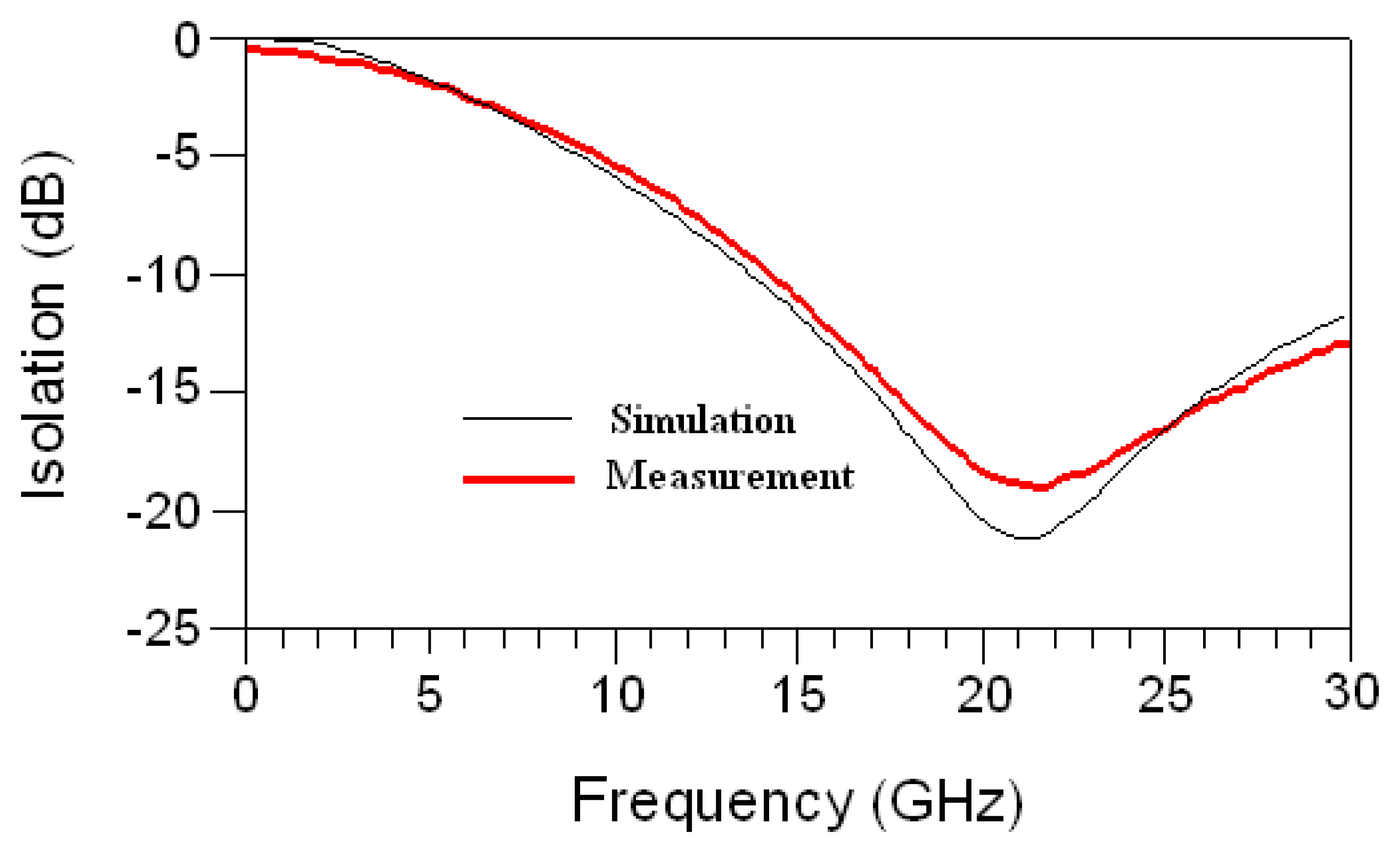
The switch was in the actuated state or ‘off’ state when applying a driving voltage of 13 V. Figure 13 shows the isolation (S21) of the switch in the actuated state. The experimental results revealed that the switch had an isolation of 19 dB at 21 GHz. As shown in Figure 13, the measured results of the isolation are in good agreement with the simulated results of the isolation. This means that the simulated results of equivalent circuit (Figure 6) are reliable.
The micromechanical switch proposed by Dai et al. [12] was fabricated on a silicon substrate using the CMOS-MEMS technique, in which the switches had an isolation of about 5 dB at 21 GHz. Comparing with Dai et al. [12], the switch of this work used the series inductors to enhance the performance, and the isolation of this work (19 dB at 21 GHz) exceeded that of Dai et al. [12]. On the other hand, although the isolation and insertion loss of Zheng et al. [4], Chang et al. [5] and Park et al. [6] exceeded that of this work, the actuation voltage of the work was lower than that of Zheng et al. [4] and Chang et al [5].
5. Conclusion
A micromechanical RF switch integrated with series inductors has been fabricated using the commercial CMOS process and a post-process. The series inductors could enhance the performances of the switch. The experimental results revealed that the isolation of the switch exceeded our previous studies [9, 12]. The micromechanical switch required only one wet etching post-process to release the suspended structures. Experiments showed that the actuation voltage of the switch was 13 V, and the switch had an insertion loss of 1.7 dB at 21 GHz and an isolation of 19 dB at 21 GHz. An equivalent circuit was proposed to evaluate the insertion loss and isolation of the switch, in which the simulated results were agreeable to the measured results. The displacement and stress of the switch were simulated by CoventorWare. The simulated results showed that the pull-in voltage of the switch was about 13 V, in which the value was in good agreement with the tested value.
Acknowledgments
The authors would like to thank National Center for High-performance Computing (NCHC) for chip simulation, National Chip Implementation Center (CIC) for chip fabrication and the National Science Council of the Republic of China for financially supporting this research under Contract No NSC 96-2221-E-005-081.
References
- Tilmans, H.A.C.; De Raedt, W.; Beyne, E. MEMS for wireless communication: ‘From RF-MEMS components to RF-MEMS-SiP’. J. Micromech. Microeng. 2003, 13, S139–S163. [Google Scholar]
- Hah, D.; Yoon, E.; Hong, S. A low voltage actuated microelectromechanical switch for RF application. Jpn. J. Appl. Phys. 2001, 40, 2721–2724. [Google Scholar]
- Goldsmith, C.; Randall, J.; Eshelman, S.; Lin, T.H.; Denniston, D.; Chen, S.; Norvell, B. Characteristics of micromachined switches at microwave frequencies. IEEE MTT-S Int. Microwave Symp. Dig. 1996, 1141–1144. [Google Scholar]
- Zheng, W. B.; Huang, Q.A.; Liao, X.P.; Li, F.X. RF MEMS membrane switches on GaAs subtrates for x-band applications. J. Microelectromech. Syst. 2005, 15, 464–471. [Google Scholar]
- Chang, C.; Chang, P. Innovative micromachined microwave switch with very low insertion loss. Sen. Actuators A 2000, 79, 71–75. [Google Scholar]
- Park, J.Y.; Kim, G.H.; Chung, K.W.; Bu, J.U. Monolithically integrated micromachined RF MEMS capacitive switches. Sen. Actuators A 2001, 89, 88–94. [Google Scholar]
- Kim, J.W.; Takao, H.; Sawada, K.; Ishida, M. Integrated inductors for RF transmitters in CMOS/MEMS smart microsensor systems. Sensors 2007, 7, 1387–1398. [Google Scholar]
- Cheng, Y.C.; Dai, C. L.; Lee, C.Y.; Chen, P.H.; Chang, P.Z. A circular micromirror array fabricated by a maskless post-CMOS process. Microsys. Technol. 2005, 11, 444–451. [Google Scholar]
- Dai, C.L.; Peng, H.J.; Liu, M.C.; Wu, C.C.; Hsu, H.M.; Yang, L.J. A micromachined microwave switch fabricated by the complementary metal-oxide semiconductor post-process of etching silicon dioxide. Jpn. J. Appl. Phys. 2005, 44, 6804–6809. [Google Scholar]
- Senturia, S.M. Microsystem Design; Kluwer Academic: Boston, MA, 2001; p. 196. [Google Scholar]
- Koolen, M.C.A.M.; Geelen, J.A.M.; Versleijen, M.P.J.G. An improved de-embedding technique for on-wafer high-frequency characterization. IEEE Proc. Bipolar/BiCMOS Circuit. Technol. Meet. 1991, 188–191. [Google Scholar]
- Dai, C.L.; Hsu, H.M.; Tsai, M.C.; Hsieh, M.M.; Chang, M.W. Modeling and fabrication of a microelectromechanical microwave switch. Microelectron. J. 2007, 38, 519–524. [Google Scholar]
Figure 1.
Structures and dimensions of (a) micromechanical RF switch, (b) spring, and (c) inductor.

Figure 2.
Displacement distribution of the switch.
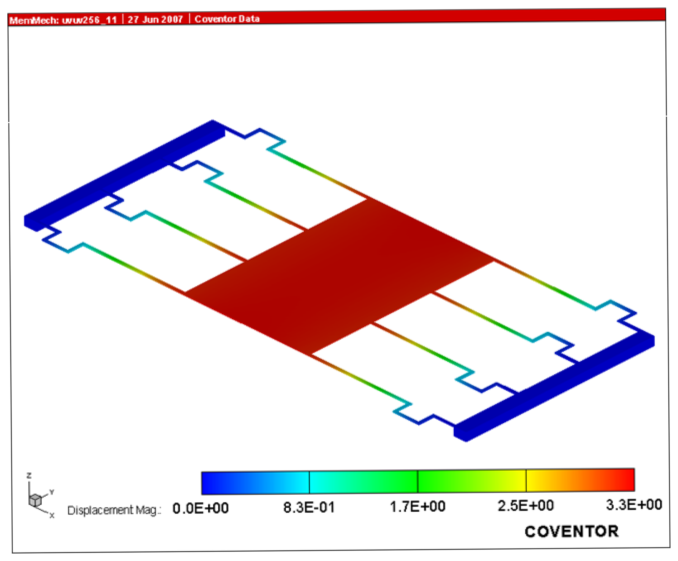
Figure 3.
Applied voltage versus membrane displacement.
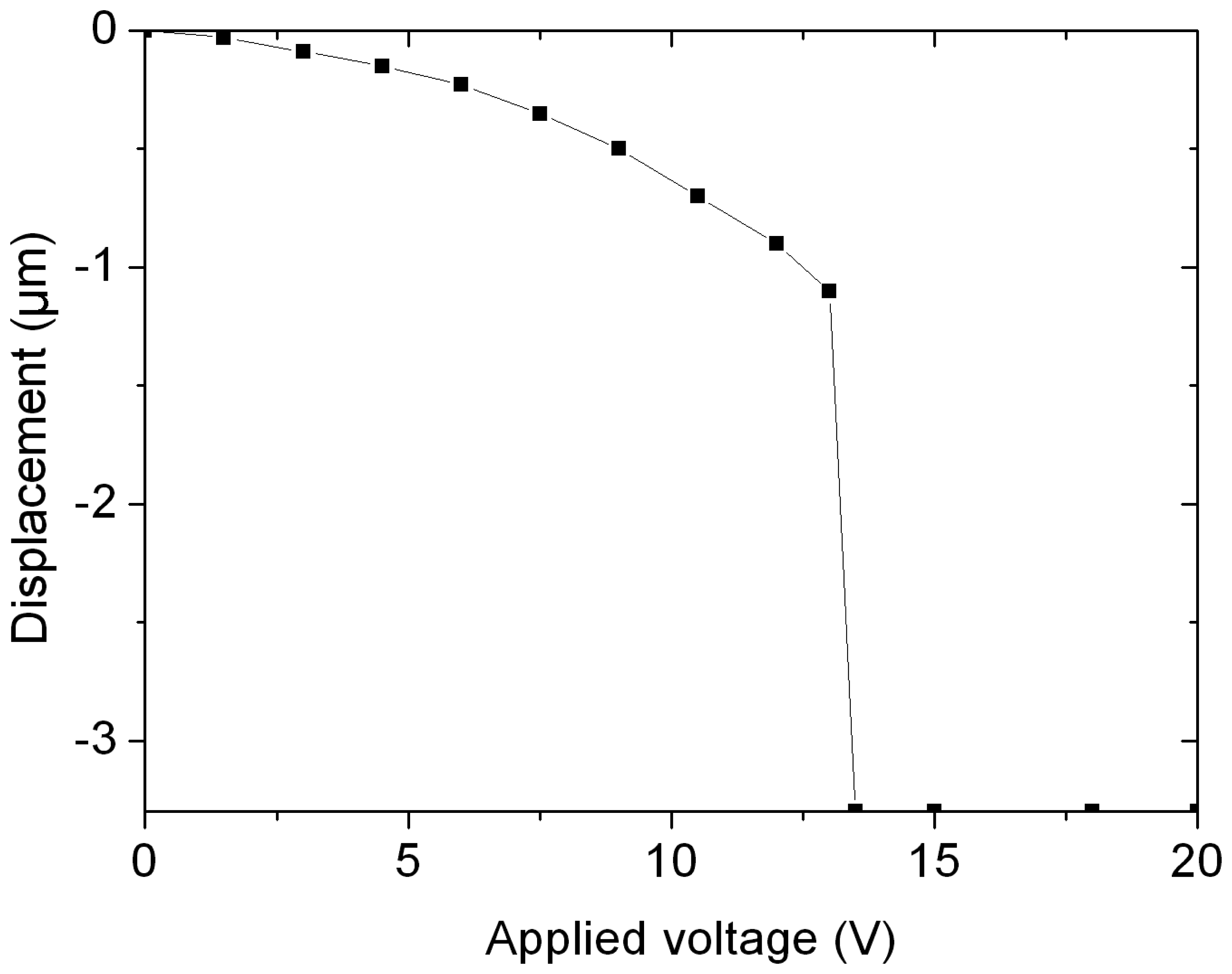
Figure 4.
Stress distribution of the switch.

Figure 5.
Simulation of the CPW characteristic impedance.

Figure 6.
Equivalent circuit of the switch.
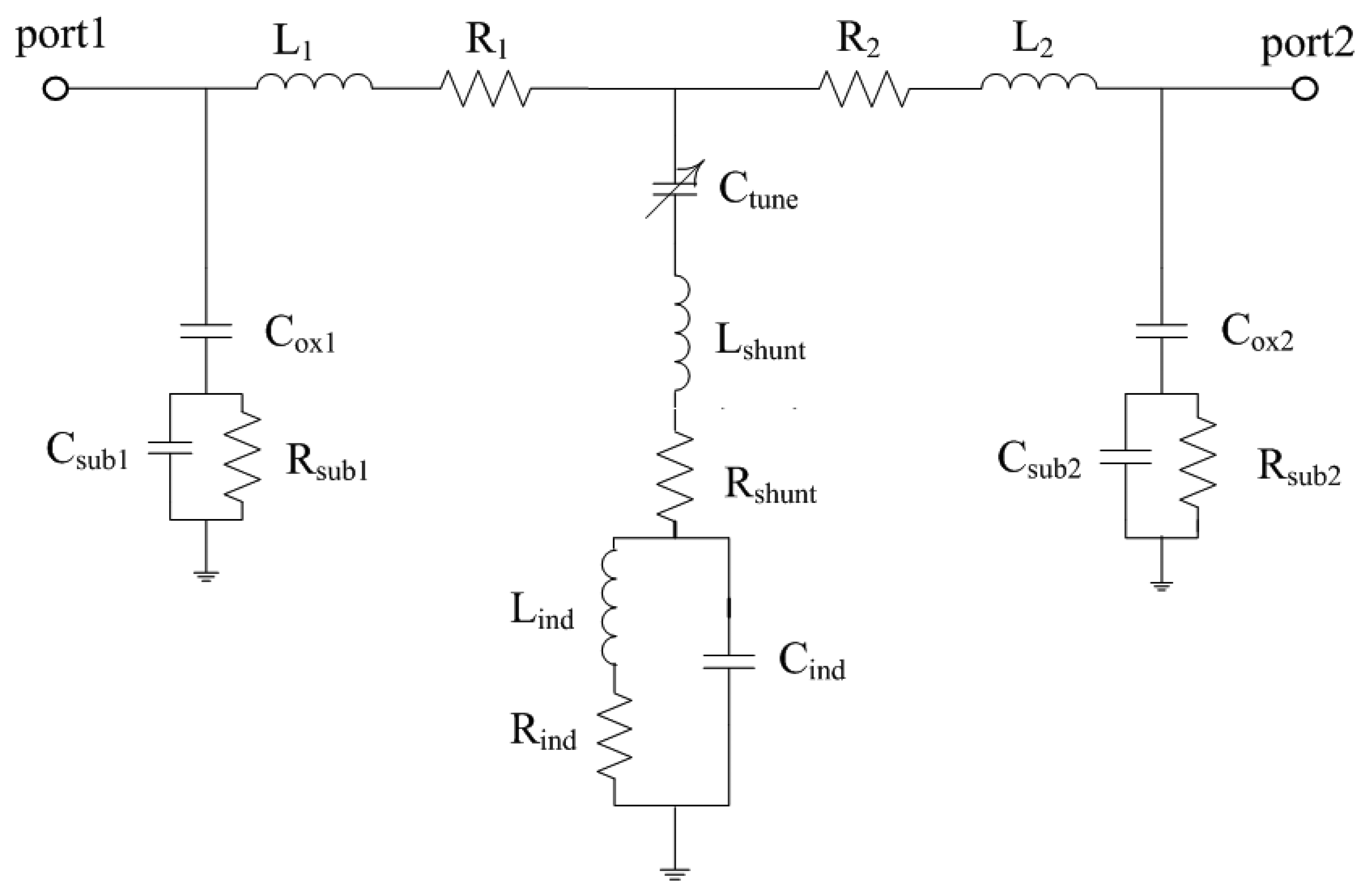
Figure 7.
Simulation of insertion loss for the switch.

Figure 8.
Simulation of isolation for the switch.

Figure 9.
Process flow of the switch: (a) after the CMOS process and (b) after the post-process.
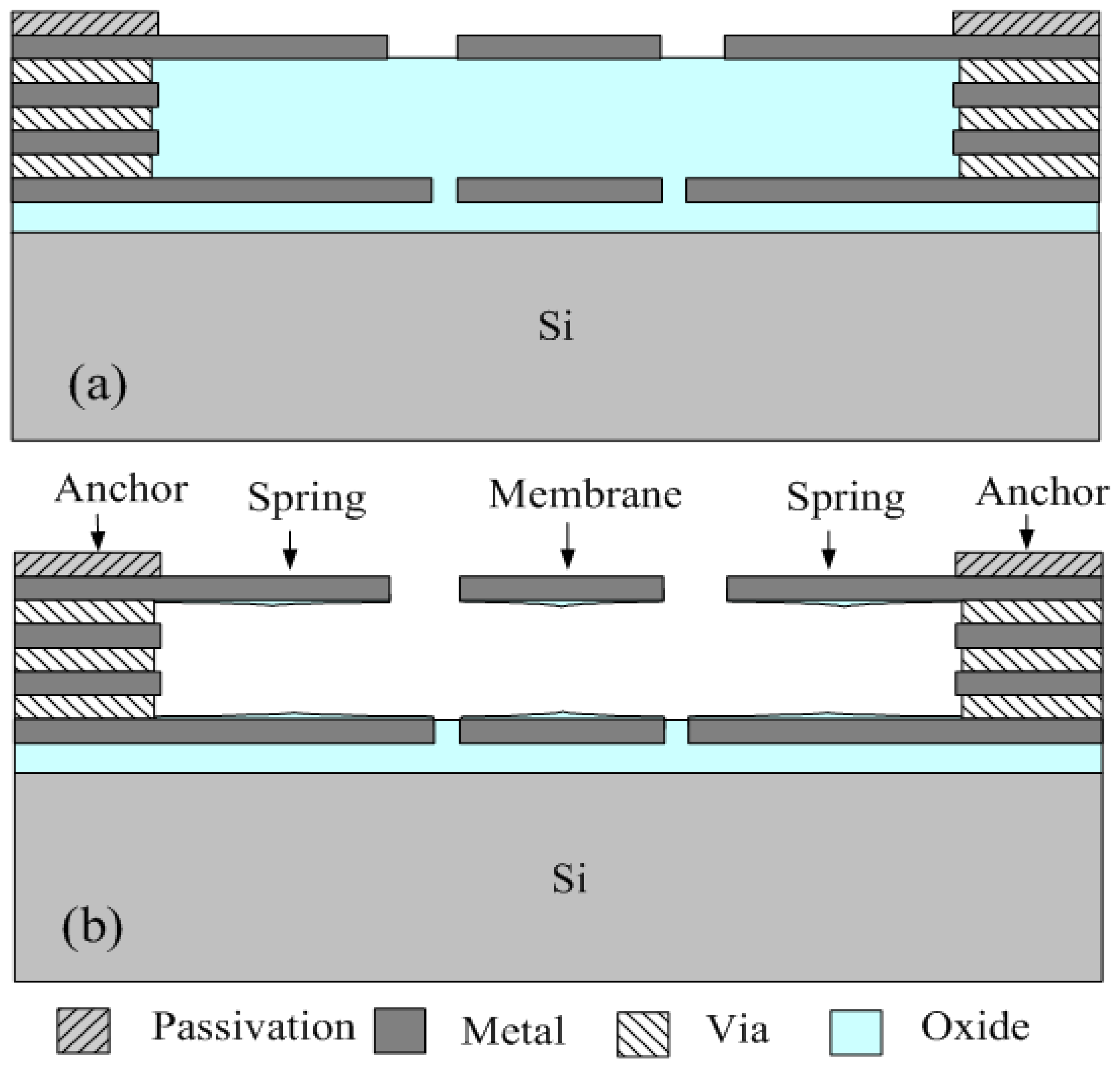
Figure 10.
SEM image of the switch after the CMOS process.
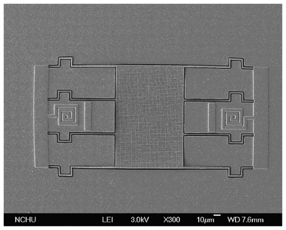
Figure 11.
Insertion loss of the switch.

Figure 12.
Return loss of the switch.
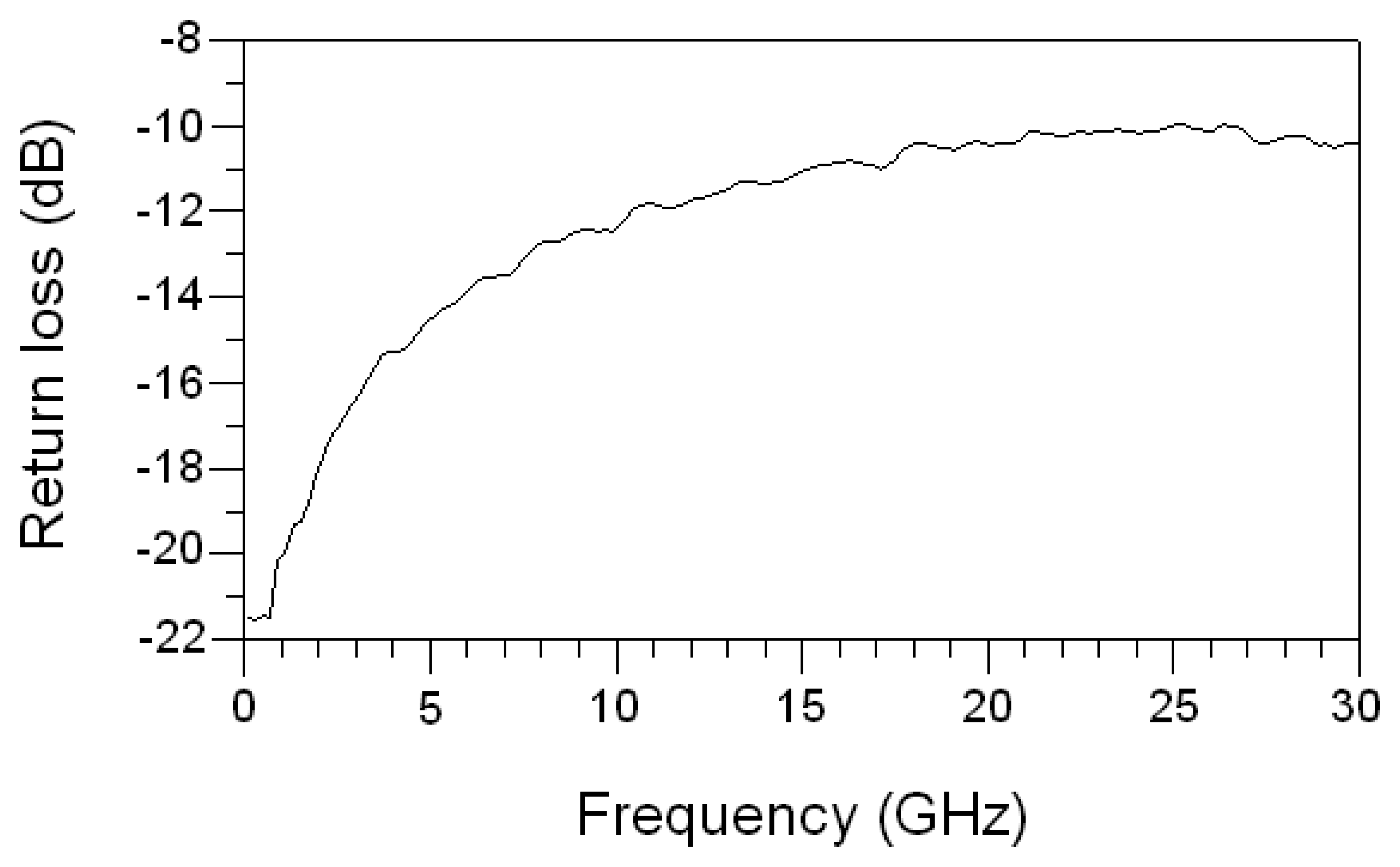
Figure 13.
Isolation of the switch.

| Properties | ‘on state’ | ‘off state’ |
|---|---|---|
| Ctune (fF) | 44 | 885 |
| Lshunt (pH) | 25.5 | 25.5 |
| Rshunt (Ω) | 0.175 | 0.175 |
| Cind (fF) | 1.4 | 1.4 |
| Lind (pH) | 56.3 | 56.3 |
| Rind (Ω) | 1.2 | 1.2 |
| L1/L2 (pH) | 28 | 28 |
| R1/R2 (Ω) | 0.04 | 0.04 |
| Cox1/Cox2 (fF) | 30 | 30 |
| Csub1/Csub2 (fF) | 1.05 | 1.05 |
| Rsub1/Rsub2 (Ω) | 350 | 350 |
© 2007 by MDPI ( http://www.mdpi.org). Reproduction is permitted for noncommercial purposes.
Share and Cite
MDPI and ACS Style
Dai, C.-L.; Chen, Y.-L. Modeling and Manufacturing of Micromechanical RF Switch with Inductors. Sensors 2007, 7, 2660-2670. https://doi.org/10.3390/s7112670
AMA Style
Dai C-L, Chen Y-L. Modeling and Manufacturing of Micromechanical RF Switch with Inductors. Sensors. 2007; 7(11):2660-2670. https://doi.org/10.3390/s7112670
Chicago/Turabian StyleDai, Ching-Liang, and Ying-Liang Chen. 2007. "Modeling and Manufacturing of Micromechanical RF Switch with Inductors" Sensors 7, no. 11: 2660-2670. https://doi.org/10.3390/s7112670