Studying the Effect of Deposition Conditions on the Performance and Reliability of MEMS Gas Sensors

4-9, Department of Mechanical Engineering, University of Alberta, Edmonton, AB, Canada T6G 2G8
*
Author to whom correspondence should be addressed.
Sensors 2007, 7(3), 319-340; https://doi.org/10.3390/s7030319
Submission received: 8 October 2006
/
Accepted: 16 February 2007
/
Published: 14 March 2007
(This article belongs to the Special Issue Gas Sensors)
Abstract
:In this paper, the reliability of a micro-electro-mechanical system (MEMS)-based gas sensor has been investigated using Three Dimensional (3D) coupled multiphysics Finite Element (FE) analysis. The coupled field analysis involved a two-way sequential electrothermal fields coupling and a one-way sequential thermal-structural fields coupling. An automated substructuring code was developed to reduce the computational cost involved in simulating this complicated coupled multiphysics FE analysis by up to 76 percent. The substructured multiphysics model was then used to conduct a parametric study of the MEMS-based gas sensor performance in response to the variations expected in the thermal and mechanical characteristics of thin films layers composing the sensing MEMS device generated at various stages of the microfabrication process. Whenever possible, the appropriate deposition variables were correlated in the current work to the design parameters, with good accuracy, for optimum operation conditions of the gas sensor. This is used to establish a set of design rules, using linear and nonlinear empirical relations, which can be utilized in real-time at the design and development decision-making stages of similar gas sensors to enable the microfabrication of these sensors with reliable operation.
1. Introduction
Sustaining the microfabrication process expertise and maintaining good control over the used material properties are identified as two of the major parameters that can significantly impact the development and commercialization of MEMS devices, [1-3]. The lack of certainty in the characterization of the used material properties usually leads to a lengthy and costly cycle of prototyping and testing procedures. Therefore, it is important at the design phase to establish a correlation between the deposition parameters and the device performance in actual operating conditions. This correlation can be established by modeling the effect of the variations in the materials characteristics generated at various stages of the microfabrication process [1, 4]. These correlated effects can then be packaged within applied design rules; which can certainly help in the reduction of the iterative prototyping process to achieve the desired characteristics of a specific MEMS design; consequently, reducing the overall cost of the development and prototyping process.
Since many micromachined MEMS devices are often composed of multiple layers of thin film materials, residual stresses are developed during the microfabrication process of these devices such as MEMS gas sensors, which can seriously affect their operating performance. These residual stresses can be separated into two specific types of stresses, thermal and intrinsic stresses [5-7]. Thermal stresses develop during the fabrication process due to the mismatch in the coefficient of thermal expansion between adjacent layers made of different thin film materials and during the actual operation of the microsensor. This thermally induced axial strain (εth,x) and stress (σth,x) at a position, defined by coordinates (x, z) in the thin film layer, are given by, [8].
Generally, intrinsic stresses involve any stress generated from sources such as excess vacancies, crystal dislocations, grain boundary interactions, or phase transformations, [5, 7]. The generation of intrinsic stresses is far more complicated than the thermal ones. The development of residual stresses in MEMS gas sensors might cause rupture and/or delamination of the thin film layers, which can affect the reliability and operational life of the microsensor [10, 11]. Therefore, appropriate control of these stresses to be within a minimum level is crucial for the successful and reliable operation of the MEMS-based gas sensor device analyzed.
The main purpose of the current study is to present a modeling/design framework that will assist in the correlation process of the deposition and post deposition (annealing) parameters to the gas detection sensitivity (GDS) performance and the reliability of these microfabricated MEMS-based gas sensors. This objective is accomplished by evaluating the effect of thermal, electrical, mechanical properties variations and residual stresses on the operational efficiency of the modeled MEMS-based gas sensor. And, where applicable, a correlation between these variations and various deposition parameters will then be established.
2. Gas Sensor Case Study
In this section, a detailed geometrical and operational description of the microfabricated MEMS-based gas sensor discussed in the current paper is presented.
2.1 Device Description
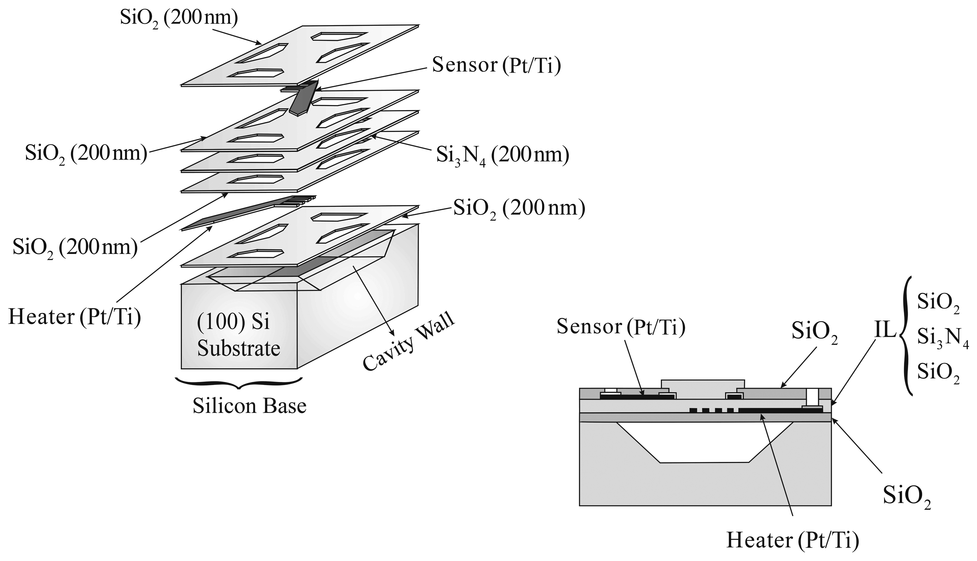
The modeled MEMS-based gas sensor is fabricated out of a silicon substrate that is followed by a thin film layer of SiO2, as shown in Figure 1. A microheater/microsensor combination is introduced in this MEMS-based gas sensing device that is prototyped using a sputtered Pt (100nm)/Ti (20nm) thin film. A multilayer of SiO2/Si3N4/SiO2 is then deposited for electrical insulation between the sensor/heater layers, while the top layer is made of SiO2 thin film. A sensitive film used to detect the presence of hazardous pollution gases is deposited in the middle area (active area) of this SiO2 top layer. The material type of the sensitive film is determined based on the gas type to be detected. The mechanism of gas detection mainly depends on measuring the change in the electrical resistance of the sensitive film, associated with the absorption of a certain amount of chemical species present in the surrounding environment, relative to its electrical resistance in air. In actual operation, an array of gas sensor cells with different sensitive film materials is used to detect different types of gases; where, calibration curves are usually established to correlate the change in the electrical resistance of the sensitive film with the gas type being sensed and the maximum or optimum operating temperature used by the gas sensor. For the studied MEMS microheater gas sensor, the optimum operation of this microsensor is achieved when the maximum temperature of the active area reaches approximately 400 °C. A detailed description of the device fabrication procedure has been reported by Mo et al. in 2001 [12].
In previous work published by the authors, the effect of varying the thermal and electrical properties and the dimensional tolerance of various thin film layers on the Gas Detection Sensitivity (GDS) performance and the thermal response of the gas sensor was introduced [4]. This study was conducted by correlating the thermal response of the gas sensor and the experimental GDS presented by Mo et al. [12]. However, correlating the proposed variations in the thermal and electrical properties to the deposition parameters was limited in that study due to the lack of thermal properties data found in the published literature; except for the thermal conductivity of SiO2 and polysilicon [13, 14]. Compared to the thermal properties, the correlation between the deposition parameters and the mechanical properties of thin films is more established in the literature; where several studies have reported on the relation between mechanical properties, such as coefficient of thermal expansion (α) [15], Young's modulus (E) [16-20], and the residual stresses (σres) [19, 21-24], and the deposition and annealing parameters used. The variation limits applied in the current study are based on the data reported in the pertaining literature that correlates these mechanical properties variations to various deposition processes and parameters. The effect of the material mechanical properties variation on the performance and operational reliability of the gas microsensor can then be investigated parametrically; where an optimum deposition parameter with reasonable tolerance limits is identified.
To solve the coupled electro-thermal problem of the MEMS-based gas sensor described in the previous section a three dimensional FE analysis is performed using ANSYS© version 10. In a steady state case, the thermal equilibrium within the sensor membrane is achieved by the balance between the heat generated in the electrical resistance, through the joule effect, and the heat loss by conduction, through the cooler supportive massive legs, and by convection, through air. As for boundary conditions (BC), the temperature at the external edges of the sensor is set to hold at room temperature [4]. On the upper surface of the membrane, the heat is dissipated through convective, conductive and thermal radiation exchange with the surrounding air. And, due to the miniature scale of the heated structures, the convection losses are considered negligible in this case. Assuming low air flow along the upper surface membrane, the air layer can then be modeled as a stagnant layer on top of this membrane. Heat exchange by conduction is calculated for this air layer based on the layer thickness (d) of 0.3 μm modeled above the membrane. Finally, the surfaces encountering heat exchange through radiation are considered as gray emitters with an emissivity of 0.5, [4].
The analyzed FE model and resulting temperature distribution for the top layer of the sensor are shown in Figure 2. For this case, an earlier FE mesh sensitivity analysis was carried out, and concluded that for a 3D model of the gas sensor, a minimum of 450,000 elements with about 300,000 DOF is required to achieve mesh independent solution. This large mesh size is often used in multiphysics problems that involves MEMS sensors and is usually attributed to the analysis complexity; which in this case include nonlinearities due to radiation, temperature dependence of the material properties and geometrical complications due to the high aspect ratio of the sensor geometric model. In order to model the various design parameters of the MEMS gas sensors, a parametric analysis consisting of approximately 625 runs (ntotal) is conducted. The computational cost, in time, for each of these coupled electro-thermal analysis runs has reached up to 19.5 hrs on a Dual Processor Pentium IV Xeon System 2.66GHz processor work station, which shows the high computational expense involved in performing these types of parametric studies. Therefore, an automated substructuring code was developed and successfully used in the current study to reduce the computational cost involved in simulating this coupled multiphysics FE problem by up to 76 percent. The power-temperature relationship was calculated using the developed substructured coupled multiphysics FE technique and compared with experimental measurements reported in [12], a case where Pt/Ti is utilized as the microheater material, and shown in Figure 3; where,
refer to the maximum operating temperature in the active area of the gas sensor. Figure 3 shows a good agreement between the outcome of the developed substructuring code and the experimental results. A more detailed explanation of the substructuring technique and its full validation has been reported in previously published work [4, 25, 26].
3. Design/Modeling Framework of the MEMS-Based Gas Sensor
The investigated MEMS-based gas sensor is designed and modeled using the simulation framework shown in Figure 4. Starting from a preliminary design of the gas sensor, an investigation of the deposition process with different specifications for the various thin film layers is conducted. The data used at the first stage include the effect of the residual stresses and the variations in the material properties corresponding to different deposition processes and parameters. At this phase, a preliminary estimation is focused on investigating the reduction of the residual stresses using annealing, where this preliminary assessment is based on the application of this MEMS-based gas sensor.
For other MEMS devices such as MEMS optical switches or micro devices that involve moving components, controlling the residual stress within a small range with minimum average is essential for the successful operation of these micro devices [2, 3, 11, 27]. In the case of MEMS-based gas sensors, except optical gas sensors, post process annealing might not be required, and might actually alter some of the desired mechanical, thermal and electrical properties of the fabricated thin films, [28-31]. A later assessment of the fabrication-related residual stresses can still be conducted at the final phases of the gas sensor design, based on the final levels of operational stresses and their effect on the reliability and fatigue life of this sensor. In the second phase of this work, the variations in the material properties and geometric parameters are applied to the MEMS-based gas sensor thin film layers, where these variations effect on the overall performance and the operation reliability of the sensor are then investigated. Finally, necessary design modifications and various deposition/post deposition parameters are recommended based on the outcome of the two phases.
4. Thermal Fatigue Analysis of the MEMS-Based Gas Sensor
Although fatigue failure of thin film structures has not been the main focus in most of the research work reported in the pertaining literature, recent studies confirmed that micro-scale structural thin films are susceptible to premature failure at stress amplitudes as low as half the fracture strength of these films materials, [32, 33]. The investigated MEMS-based gas sensor is subject to cyclic thermal loading caused by the residual stresses generated at the microfabrication process and the actual operational thermal stress. In this section, the effect of thin film material property variation on the fatigue life of the gas sensor is presented. A list of the studied parameters, as well as the range of their applied variations is shown in Table 1, [15, 16-20, 34, 35]. The parameters, p, T, G and DR denote the deposition pressure, deposition temperature, the SiH2Cl2/NH3 ratio and the deposition rate, respectively.
To the best of the authors' knowledge, no reported value for the ultimate strength of Pt/Ti thin film material could be found in the available literature. Nevertheless, Strikar and Spearing reported in 2003 [36] similar cases, where the value of the ultimate strength for the bulk material is used as a conservative limit for the tensile ultimate strength. In this work, the value for the ultimate tensile strength of Pt/Ti was calculated from the measured values of the Vickers hardness for the “as cast” Pt/Ti reported by Biggs et al. in 2005 [37]. As shown later in Section 4.1, the operational stress level for Pt/Ti (microheater/sensor material) is found to be higher than the ultimate tensile fracture strength. This would suggest the occurrence of rupture or delimitation of the Pt/Ti thin film, which is in good agreement with reported observations in previous experimental studies presented in the literature, [29, 30, 38]. Therefore, the utilization of p-type heavily boron doped polysilicon as a heater material was recommended to be used in the current case. However, the increase in the power consumption resulting from the use of the polysilicon as a microheater material is an emerging concern. Another concern is mainly related to the shifting in the thermal response (αT) and the performance GDS (ψsen) of the gas sensor with the variation in the electrical resistivity of polysilicon. Using the same procedure described in [4], a correlation of the variation in αT and ψsen with the variation of the polysilicon resistivity is derived.
The numerical results previously shown in Figure 3, indicate that the suggested design modification would result in an increase in the power consumption (P) at the optimum operating temperature (
) of only 10 percent (i.e. an increase of 1 mW, P ≈ 9.9 mW with p-type heavily boron-doped polysilicon compared to P ≈ 9 mW with Pt/Ti heater). However, a matching improvement of 13 percent in the performance sensitivity and a greater reduction in the operational stress levels will be achieved with this modified design.
4.1. Maximum stress variation with the thermal, electrical and mechanical properties
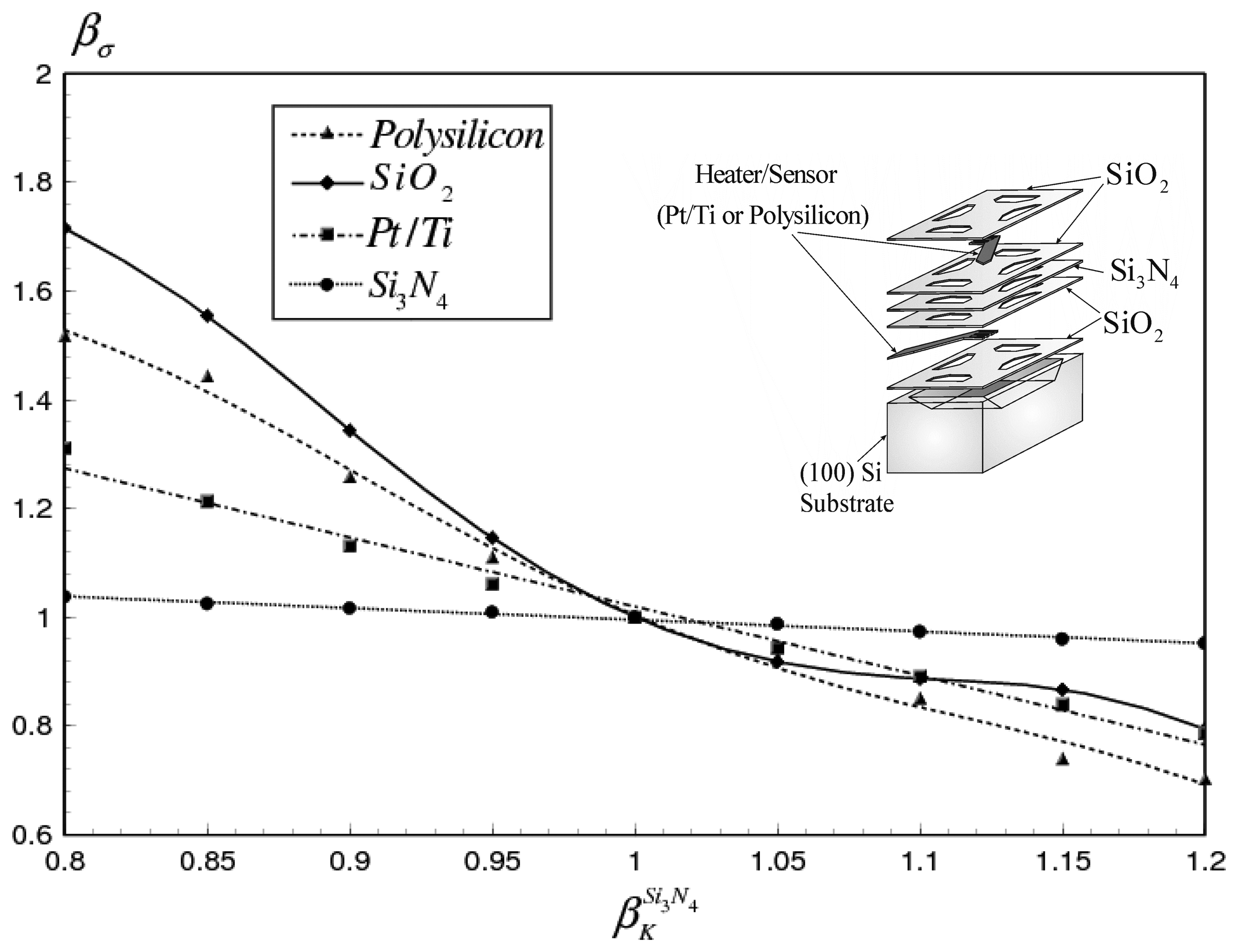
The structural analysis presented in this paper study the effect of the variation in the thermal, electrical and mechanical properties on the maximum generated stress in all the different thin film layers composing the studied MEMS-based gas sensor. In the electrothermal analysis, only the conductivity of Si3N4 and the resistivity of the heater material (Pt/Ti or polysilicon) were found to generate a significant effect on the thermal response of the modeled MEMS-based gas sensor [4]. Therefore, only the variations of these thermal/electrical parameters were considered in the current case. The variations of the maximum generated stress in various thin film layers versus the uncertainty in the thermal conductivity of Si3N4 and the electrical resistivity of Pt/Ti and polysilicon are shown in Figures 5, 6 and 7, respectively.
The dimensionless term βσ (stress factor) indicate the ratio between the actual maximum operational stress (σAmax) and the nominal maximum stress (σNmax), which is the stress value before varying any property. The values for σNmax and its ratio relative to the ultimate fracture strength (Sut) for different thin film materials are shown in Table 2. Similarly, the dimensionless terms,
,
and
indicate the ratios between the actual and nominal values of the thermal conductivity of Si3N4 and the electrical resistivity of Pt/Ti and polysilicon, respectively.
As shown in Figure 5, the variation in the thermal conductivity of Si3N4 generates a significant variation in the maximum operational stress level ranging from +72 to -12 percent for SiO2, +28 to −14 percent for Pt/Ti, and +46 to −24 percent for polysilicon. A less significant variation of ± 5 percent is noticed for the maximum stress of Si3N4. The former variation values can be attributed to the high variation generated in the thermal response of the sensor with the applied power, and the combined effect of the value for the coefficient of thermal expansion (e) for the thin film layer material and its proximity to the active area. Results shown in Figure 5 were fitted linearly using Equation (2) for Si3N4 and Pt/Ti. A polynomial fitting is used for SiO2 and polysilicon and presented in Equation (3) below.
A similar result is obtained for βσ with the variation of the electrical resistivity of Pt/Ti and polysilicon. As shown in Figure 6, the variation in
results in a significant effect on the maximum operational stress level ranging from +88 to -40 percent for SiO2, +42 to −32 percent for Pt/Ti, and ± 8 percent for Si3N4. Results shown in Figure 6 were linearly fitted as depicted in Equation (4) for Si3N4 and Pt/Ti; and with polynomial fitting using Equation (5) for SiO2 as follows
Equations (4) and (5) constants and the average root mean square error (RMS) of the curve fitting are listed in Tables 3 and 4, respectively. A less significant effect can be noticed with the variation in the maximum operational stress and
due to the smaller variation in the thermal response, as shown in Figure 7. Results shown in this Figure are fitted linearly with Equation (6) for Si3N4 and using polynomial fitting presented in Equation (7) for SiO2 and polysilicon as follows
Equations 6 and 7 constants and the average root mean square error (RMS) of the curve fitting are listed in Tables 3 and 4, respectively. The dimensionless terms βe and βE indicate the ratios between the actual and nominal values of the coefficient of thermal expansion (e) and Young's modulus (E) for different thin film materials, respectively. The variation of the stress factor (βσ) for different thin film materials with βe for Si3N4 is shown in Figure 8.
The variation of
was found to generate a significant variation in maximum stress of the Si3N4 layer ranging from +33 to -13 percent. A less significant variation range of 0 to +5 percent is calculated for other thin film materials. Similarly, the same effect can be noticed for the variation of βe using other thin film materials, as shown in Figures 9, 10 and 11. Moreover, the presented results shows that the variation in the coefficient of thermal expansion for an individual thin film material results in a significant variation in the maximum stress generated within this thin film layer. The stress level in the other thin film layers of the analyzed MEMS-based gas sensor does not seem to be impacted as strongly as the layer at which the thermal expansion coefficient was varied. Equation (8) is a polynomial fitting of the obtained numerical results expressing the relation between the stress factor (βσ) of Si3N4 and
. Also, the relation between the stress factor (βσ) for Pt/Ti, polysilicon and SiO2 and βσ is expressed linearly by Equation (9) as follows
A list for Equation (8) constants and the average RMS of the fitted curve are shown in Table 4; where, βe in Equation (9) represents the variation in the coefficient of thermal expansion for different materials used for the thin film layers. Similarly, a list of the constants in Equation (9) for Pt/Ti, polysilicon and SiO2 and the average RMS of the fitted curve are shown in Table 3.
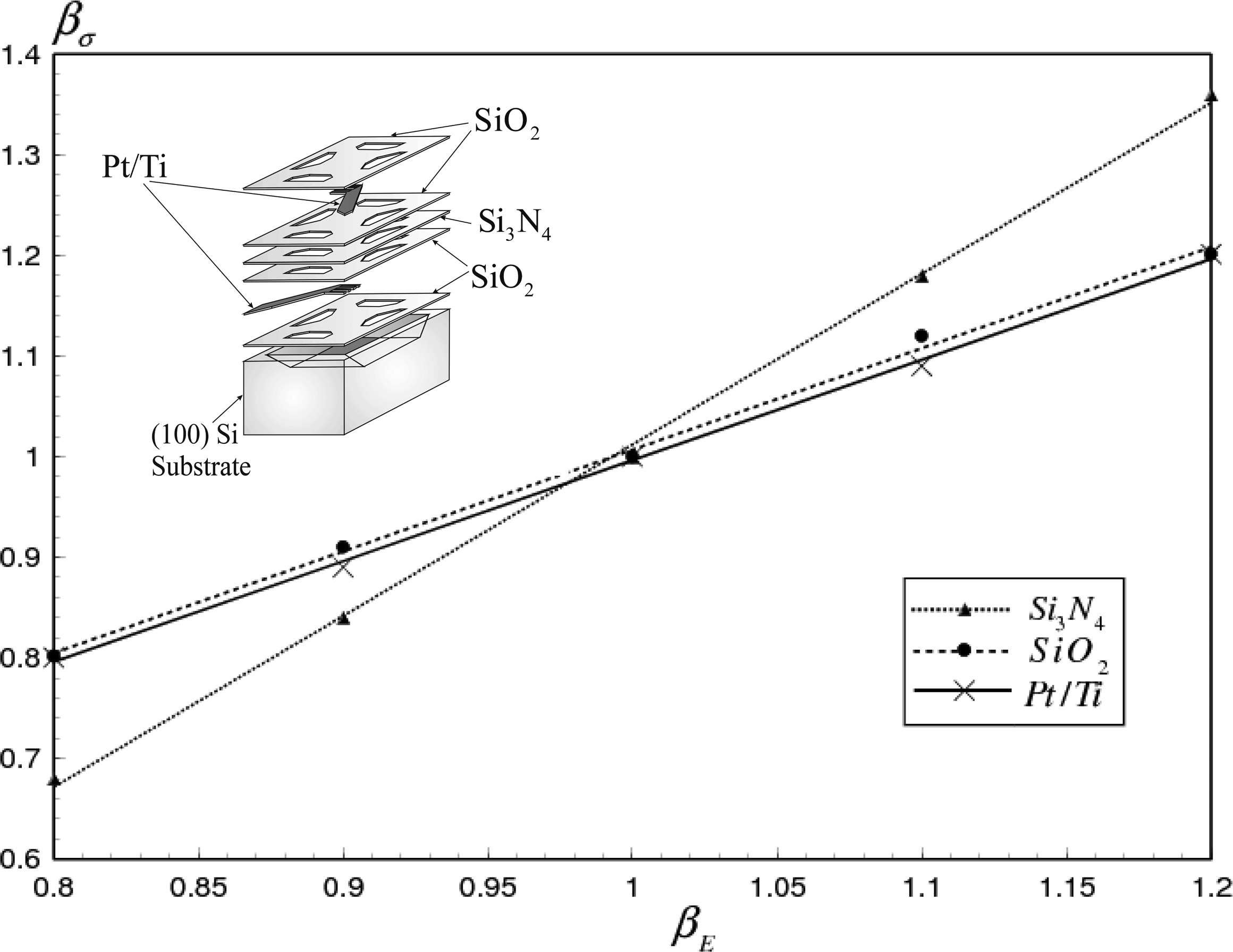
The variation of the stress factor (βσ) with βE is calculated and shown in Figure 12. It can be seen that the variation in Young's modulus only generates a variation in the maximum stress level of the thin film materials at the individual layer level. As shown in Figure 12, the change of βE generates a variation in the maximum stress level ranging from +36 to −32 percent for Si3N4, -19 to 16 percent for SiO2 and −20 to 14 percent for Pt/Ti. Results shown in Figure 12 were linearly fitted using Equation (10) to express the relation between βσ and βE for different thin film materials.
4.2 Fatigue life of the MEMS-based gas sensor
Results from the structural analysis, carried out in the last section, indicate that the value of σNmax for Pt/Ti was approximately twice the ultimate fracture strength, which suggests the possibility of rupture, chipping or delimitation of the used Pt/Ti thin film layer. Based on this result, an investigation was conducted to replace the Pt/Ti with p-type heavily boron-doped polysilicon as the material for the heater and sensing layers. The fracture strength and coefficient of thermal expansion of Polysilicon is higher by an order of magnitude than Pt/Ti which render it more compatible with neighboring thin film layers. This explains the reduction in the operational stress in the heater material by using polysilicon rather than Pt/Ti. Further investigation for other thin film materials indicates that the operating stress levels are safe enough with respect to static failure. The next step here is to investigate the fatigue life for these thin film layers under thermal cyclic loading.
The microheater layer of the studied gas sensor is subjected to a state of fluctuating stress with values ranging from the value of the residual stress induced to the value of this sensor layer operating thermal stress. An equivalent value for a completely reversed loading should be calculated to be able to estimate the fatigue life using the S-N curve for this layer material.
The value of the equivalent alternating stress can be calculated using Goodman's curve, where the values for the actual mean and alternating stresses are calculated as follows.
An initial investigation of the various thin film materials used at different values of experienced residual stress, shows that the calculated equivalent alternating stress is within a safe level and not affected by fatigue failure, except for Si3N4 (
> 0.5 Sut), as shown in Table 2. The largest variation of σAmax for Si3N4 was found to occur with
(+33 to -13 percent), as shown in Figure 8, and
(+36 to −32 percent), as shown in Figure 12. Therefore, only the variation of
for Si3N4 with the parameters mentioned above is discussed here. The dimensionless terms
and δσres denote the ratios of
and σres to Sut, respectively.
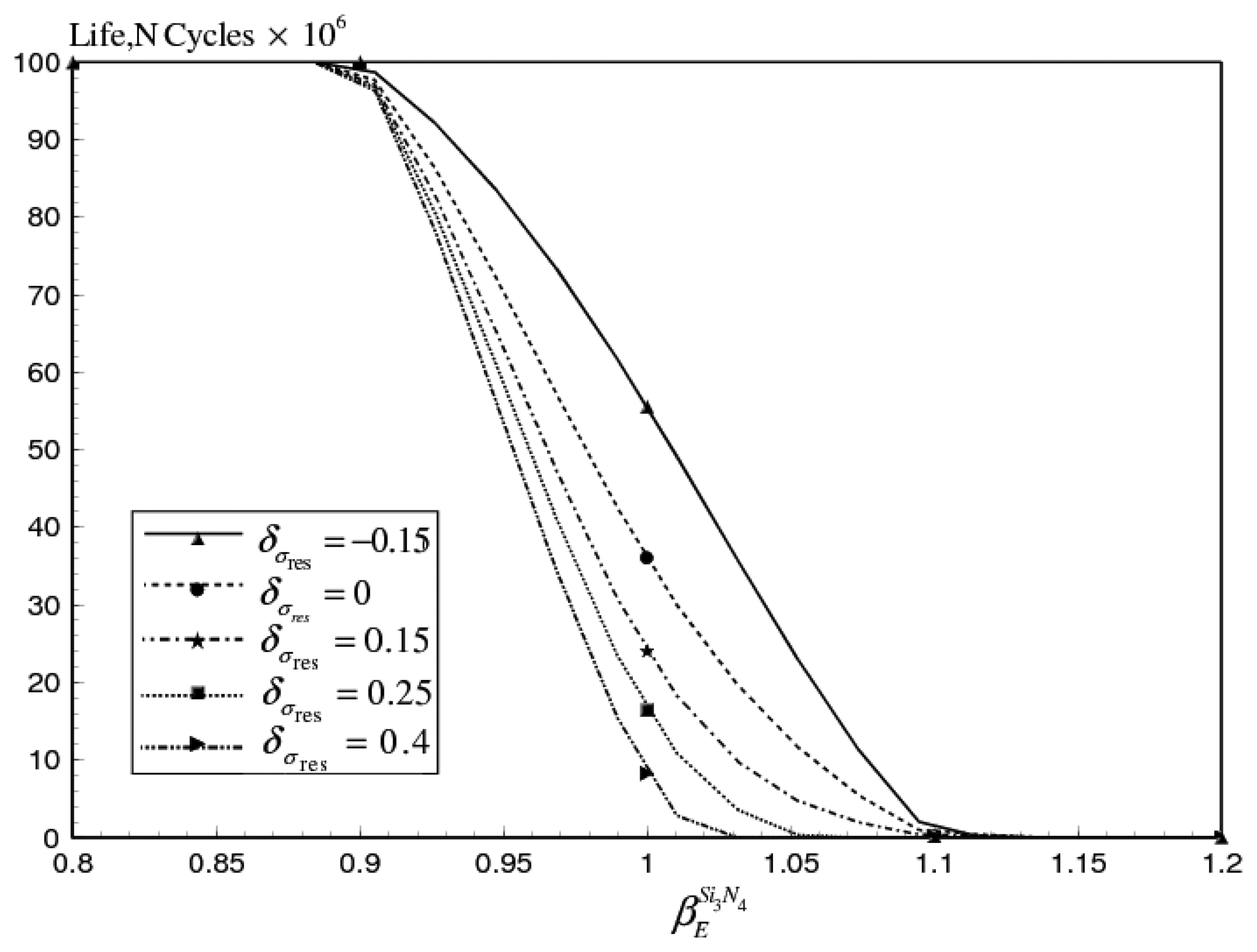
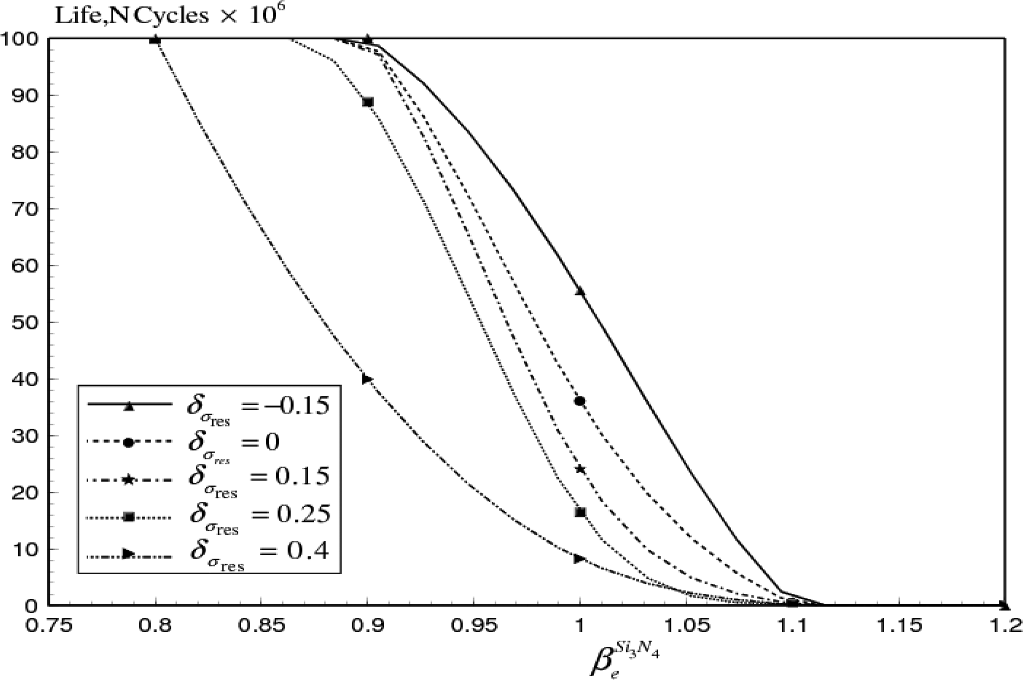
The relation between
the number of load cycles representing fatigue life, N, and
at different δσres values is shown in Figures 13 and 14, respectively. Lower values for
and higher N is found when δσres = −0.15 (i.e. σres = -60 MPa). This indicates that the analyzed gas sensor is not going to experience fatigue failure while
is in the range of 0.8 to 0.87 regardless of the value of δσres, while outside this range the sensor experience fatigue failure at relatively shorter operational life cycles.
The same effect is obtained when varying
and N with
at different values of δσres, as shown in Figures 15 and 16, respectively. However a wider range for
variation (0.8 to 0.95) is found to provide safer operating conditions under thermal cyclic loading regardless of the value of δσres.
5. Conclusions
In this paper, the reliability of MEMS-based gas sensors has been investigated using 3D coupled multiphysics FE analyses. The coupled field analysis involved a two-way sequential electro-thermal fields coupling and a one-way sequential thermal-structural fields coupling. An automated sub structuring code was developed to reduce the computational cost involved in this coupled multiphysics FE analysis by up to 76 percent. Results from the developed substructured multiphysics model were found to be in good agreement with experimental measurements, previously reported in the literature. The substructured multiphysics model was then used to conduct a parametric study of the MEMS-based gas sensor performance in response to the variations expected in the thermal and mechanical characteristics of thin films layers composing the sensing MEMS-based device generated at various stages of the microfabrication process. The results of this parametric study are then used to establish, with good accuracy, a set of design rules, using linear and nonlinear empirical relations, which can be utilized in real-time at the design and development decision-making stages of similar gas sensors to enable the microfabrication of these sensors with reliable operation. The results of this parametric study indicated that the use of Pt/Ti as the material for the heater/sensing layer in the investigated gas sensor can result in stress levels exceeding its ultimate fracture strength, which was in good agreement with experimental observations reported in literature. Therefore, p-type heavily boron-doped polysilicon is recommended, instead, to be used in fabricating the heater/sensing layer in this gas sensor. The suggested design modification would result in an increase in the power consumption of only 10 percent. However, a matching improvement of 13 percent in the performance sensitivity and a greater reduction in the operational stress levels will be achieved with this modified design. Except for Si3N4, all thin film materials used provided safe operating range with respect to cyclic fatigue failure at different levels of residual stresses. This will mainly eliminate the necessity of post fabrication annealing, even with the existence of slightly deformed sensing layer. This is particularly valid in the current gas sensor application, since it does not require perfectly flat thin film layers for successful operation. For Si3N4, the lowest equivalent alternating stress level was found when δσres = −0.15 (i.e. σres = -60 MPa). This residual stress value corresponds to a SiH2Cl2/NH3 ratio of approximately 5.5 and a deposition temperature of 850 oC. Regardless of the value of the residual stress, the variation of the coefficient of thermal expansion and Young's modulus for Si3N4 should be kept within −20 to 0 percent. The results presented in this work highlight the important role of modeling the uncertainties generated during the various microfabrication phases and its effect on the gas sensor sensitivity and operating conditions. This modeling process can then be integrated with the prefabrication design phase that help control these uncertainties effect on the operational reliability of this type of MEMS-based gas sensors.
Acknowledgments
The financial support of the Canadian Natural Sciences and Engineering Research Council (NSERC) through Grant No. 239188 (Principle Investigator: Dr. Walied Moussa) is gratefully acknowledged.
References
- Giridharan, M.G.; Stout, P.; Yang, H.Q.; Athavale, M.; Dionne, P.; Przekwas, A. Multi-Disciplinary CAD Systems for MEMS. Journal of Modeling and Simulations of Microsystems 2001, 2, 43–50. [Google Scholar]
- Judy, J.W. Microelectromechanical Systems (MEMS): Fabrication, Design and Applications. Smart Materials and Structures 2001, 10, 1115–1134. [Google Scholar]
- Lin, L.Y.; Goldstein, E.L. Opportunities and Challenges for MEMS in Lightwave Communications. IEEE Journal on Selected Topics in Quantum Electronics 2002, 8, 163–172. [Google Scholar]
- Sadek, K.; Moussa, W. Investigating the Effect of Deposition Variation on the Performance Sensitivity of Low-Power Gas Sensors. Sensors and Actuators B 2005, 107, 497–508. [Google Scholar]
- Chen, S.; Baughn, T.V.; Yao, Z. J.; Goldsmith, C.L. A New In Situ Residual Stress Measurement Method for a MEMS Thin Fixed-Fixed Beam Structure. Journal of Microelectromechanical Systems 2002, 11, 309–316. [Google Scholar]
- Doerner, M.; Nix, W. Stresses and Deformation Processes in Thin Films on Substrates. CRC Circuit. Rev. Solid States Material Science 1998, 14, 225–268. [Google Scholar]
- Stadtmueller, M. Mechanical Stress of CVD-Dielectrics. Journal of Electrochemical Society 1992, 139, 3269–3274. [Google Scholar]
- Belendez, T.; Neipp, C.; Belendez, A. Large and Small Deflections of a Cantilever Beam. European Journal of Physics 2002, 23, 371–379. [Google Scholar]
- Pamidighantam, S.; Puers, R.; Baert, K.; Tilmans, H.A.C. Pull-in Voltage Analysis of Electrostatically Actuated Beam Structures with Fixed-Fixed and Fixed-Free end conditions. Journal of Micromechanics and Microengineering 2002, 12, 458–464. [Google Scholar]
- Leplan, H.; Geenen, B.; Robic, J.Y.; Pauleau, Y. Residual Stresses in Evaporated Silicon Dioxide Thin Films: Correlation with Deposition Parameters and Aging Behavior. Journal of Applied Physics 1995, 78, 962–968. [Google Scholar]
- Wan, K.T.; Kogut, L. The Coupling Effect of Interfacial Adhesion and Tensile Residual Stress on a Thin Membrane Adhered to a Flat Punch. Journal of Micromechanics and Microengineering 2005, 15, 778–784. [Google Scholar]
- Mo, Y.; Okawa, Y.; Tajima, M.; Nakai, T.; Natukawa, K. Micro-machined Gas Sensor Array Based on Metal film Microheater. Sensors and Actuators B 2001, 79, 175–181. [Google Scholar]
- Paul, O.; Baltes, H. Thermal conductivity of CMOS Materials for the Optimization of Microsensors. Journal of Micromechanics and Microengineering 1993, 3, 110–112. [Google Scholar]
- Uma, S.; McConnell, A.D.; Asheghi, M.; Kurabayashi, K.; Goodson, K.E. Temperature-Dependent Thermal Conductivity of Undoped Polycrystalline Silicon Layers. International Journal of Thermophysics 2001, 22, 605–616. [Google Scholar]
- Pan, C.H. A Simple Method for Determining Linear Thermal Expansion Coefficients of Thin Films. Journal of Micromechanics and Microengineering 2002, 12, 548–555. [Google Scholar]
- Sharpe, W.N.; Turner, K.T.; Edwards, R.L. Tensile Testing of polysilicon. Experimental Mechanics 1999, 39, 162–170. [Google Scholar]
- Yi, T.; Kim, C.J. Measurement of Mechanical Properties for MEMS Materials. Measurement Science and Technology 1999, 10, 706–716. [Google Scholar]
- Sharpe, W.N.; Yaun, B.; Vaidyanathan, R. Measurements of Young's Modulus, Poisson's Ratio and Tensile Strength of polysilicon. Proceedings of the Tenth IEEE International Workshop on Microelectromechanical Systems, Nagoya, Japan; 1997; pp. 424–429. [Google Scholar]
- Denhoff, M.W. A Measurement of Young's Modulus and Residual Stress in MEMS Bridges using a Surface Profiler. Journal of Micromechanics and Microengineering 2003, 13, 686–692. [Google Scholar]
- Chaung, W.H.; Luger, T.; Fettig, R.K.; Ghodssi, R. Mechanical Property Characterization of LPCVD Silicon Nitride Thin Films at Cryogenic Temperatures. Journal of Microelectromechanical Systems 2004, 13, 870–879. [Google Scholar]
- Seok, S.; Lee, B.; Chun, K. A New Electrical Residual Stress Characterization Using Bent Beam Actuators. Journal of Micromechanics and Microengineering 2002, 12, 562–566. [Google Scholar]
- Min, Y.H.; Kim, Y.K. In Situ Measurement of Residual Stresses in Micromachined Thin films Using a Specimen with Composite-Layered Cantilevers. Journal of Micromechanics and Microengineering 2000, 10, 314–321. [Google Scholar]
- Kim, Y.J.; Allen, M.G. In Situ Measurement of Mechanical Properties of Polyimide Films Using Micromachined Resonant String Structures. IEEE Transactions on Components and Packaging Technology 1999, 22, 282–290. [Google Scholar]
- Madou, M. Fundamentals of Microfabrication; CRC Press LLC: USA, 1997. [Google Scholar]
- Noor, A.K.; Kamel, H.A.; Fulton, R.E. Substructuring Techniques Status and Projections. Computers & Structures 1978, 8, 621–632. [Google Scholar]
- Owen, D.R.; Goncalves, O.J.A. Substructuring Techniques in Material Non-Linear Analysis. Computers & Structures 1982, 15, 205–313. [Google Scholar]
- Thouless, M. D. Fracture Mechanics for Thin-Film Adhesion. IBM Journal of Resources Development 1994, 38, 367–377. [Google Scholar]
- Wrbanek, J.D.; Laster, K.L. Preparation and Analysis of Platinum Thin Films for High Temperature Sensor applications. NASA/TM-2005-213433 2005, 1–19. [Google Scholar]
- Branger, V.; Pelosin, V.; Badawi, K.F.; Goudeau, P. Study of Mechanical and Microstructural State of Platinum Thin Films. Thin solid Films 1996, 275, 22–24. [Google Scholar]
- Firebaugh, S. L.; Jensen, K.F.; Schmidt, M.A. Investigation of High-Temperature Degradation of Platinum Thin Films with an In Situ Resistance Measurement Apparatus. Journal of Microelectromechanical Systems 1998, 7, 128–135. [Google Scholar]
- Schneider, D.M.; Maibach, J.; Obermeier, E.; Schneider, D. Variations in Young's Modulus and Intrinsic Stress of LPCVD-Polysilicon due to High- Temperature Annealing. Journal of Micromechanics and Microengineering 1995, 5, 121–124. [Google Scholar]
- Muhlstein, C.L.; Ritchie, R.O. High-Cycle Fatigue of Micron-Scale Polycrystalline Silicon Films: Fracture Mechanics Analyses of the Role of Silica/Silicon Interface. International Journal of Fracture 2003, 119/120, 449–474. [Google Scholar]
- Mönig, R.; Keller, R.R.; Volkert, C.A. Thermal Fatigue Testing of Thin Metal Films. Review of Scientific Instruments 2004, 75, 4997–5004. [Google Scholar]
- Gad El Hak, M. The MEMS Handbook.; CRC Press: USA, 2001. [Google Scholar]
- Stark, B. MEMS Reliability Assurance Guidelines for Space Applications. JPL Publication, 99-1, USA 1999. [Google Scholar]
- Srikar, V.T.; Spearing, S.M. Materials Selection in Micromechanical Design: An Application of the Ashby Approach. Journal of Microelectromechanical Systems 2003, 12, 3–10. [Google Scholar]
- Biggs, T.; Taylor, S. S.; Van der Lingen, E. The Hardening of Platinum Alloys for Potential Jewellery Application. Platinum Metals Review 2005, 49, 2–15. [Google Scholar]
- Puigcorbé, J.; Vogel, D.; Michel, B.; Vilà, A.; Gràcia, I.; Cané, C. High Temperature Degradation of Pt/Ti Electrodes in Micro-Hotplate Gas Sensors. Journal of Micromechanics and Microengineering 2003, 13, 119–124. [Google Scholar]
Figure 1.
Schematic view of microheater gas sensor cell

Figure 2.
MEMS gas sensor FE model
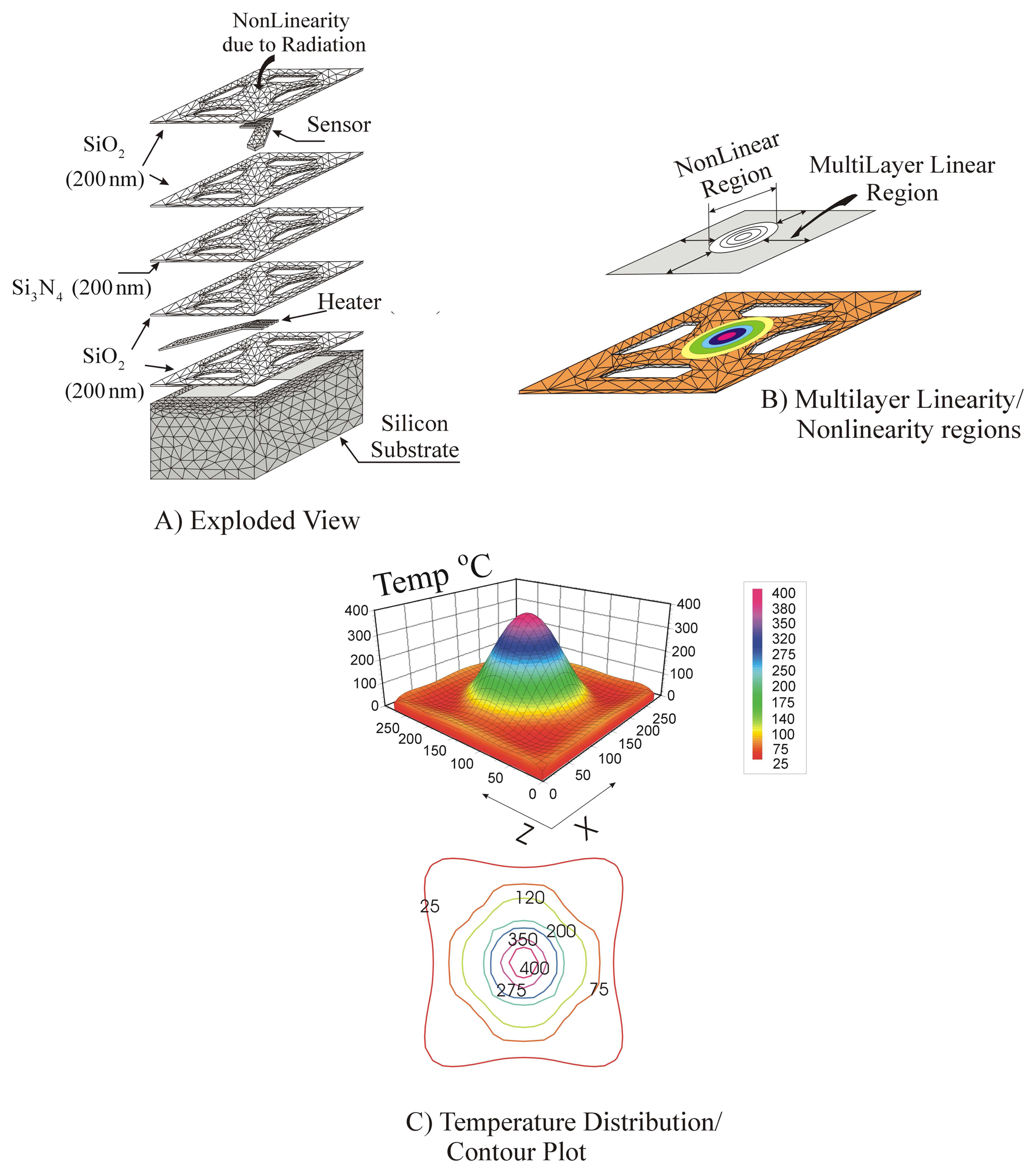
Figure 3.
Power temperature relationship for different heater material calculated with substructured coupled multiphysics analysis. Experimental measurements from Mo et al. [12]
Figure 3.
Power temperature relationship for different heater material calculated with substructured coupled multiphysics analysis. Experimental measurements from Mo et al. [12]
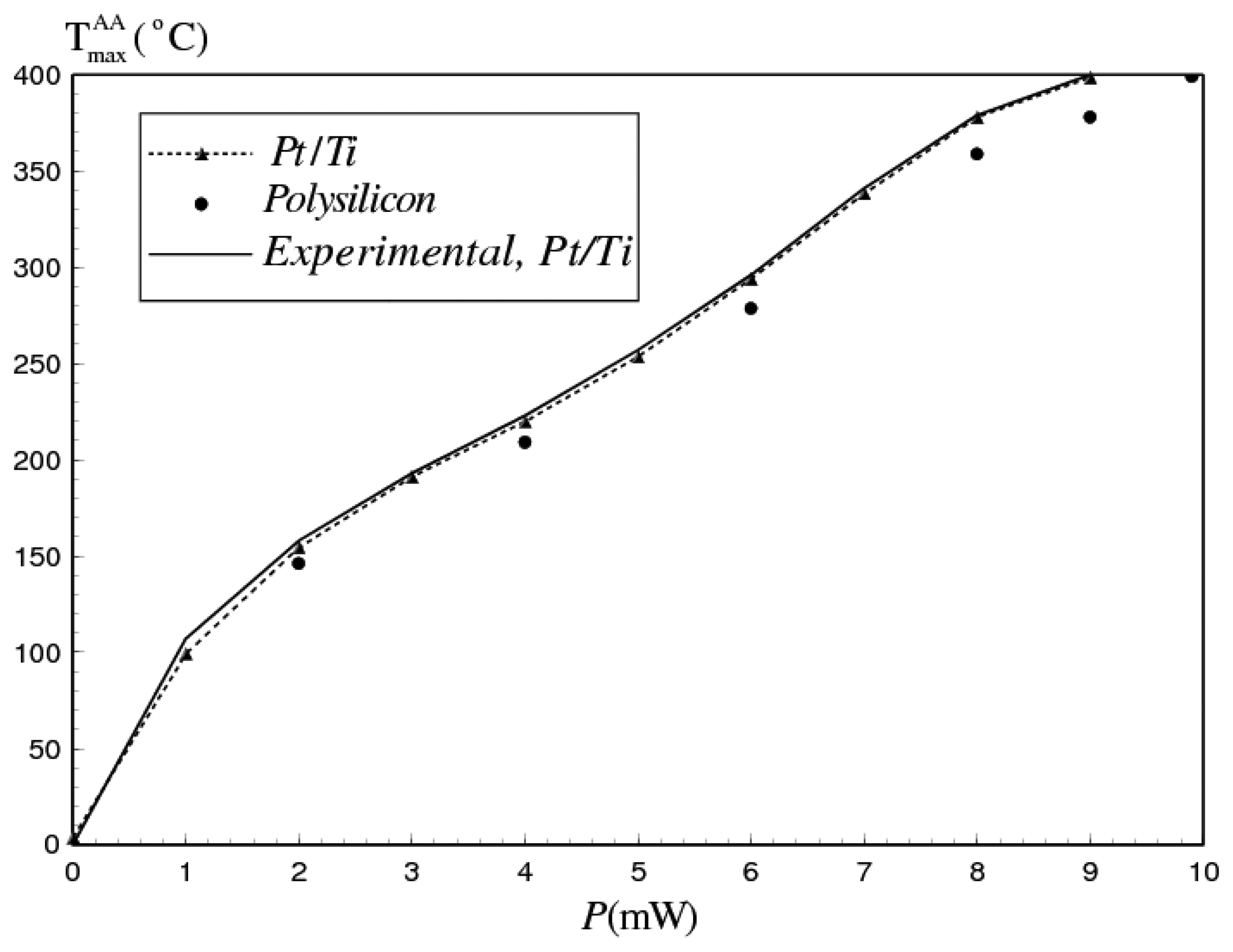
Figure 4.
Modeling/design framework
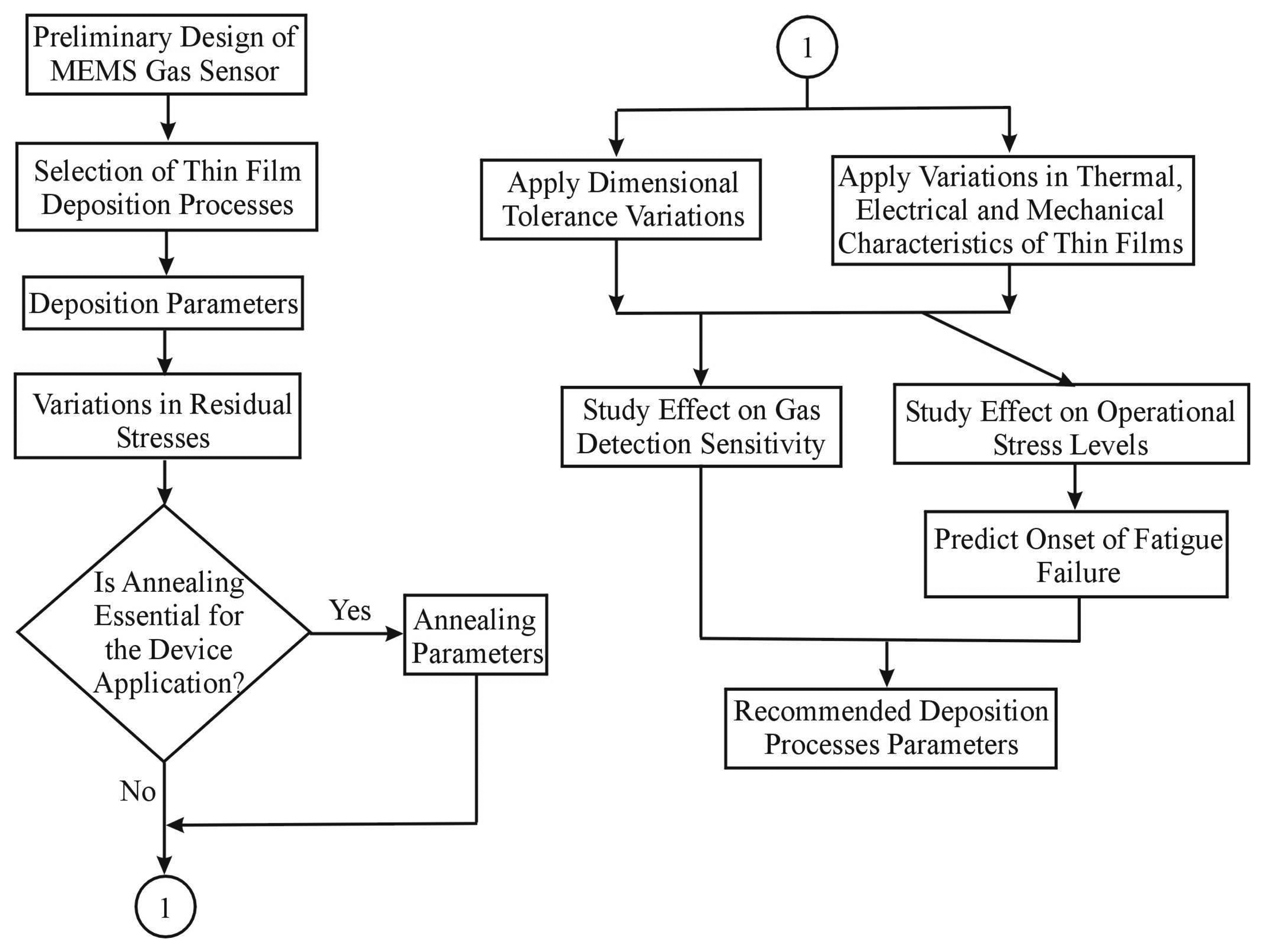
Figure 5.
Effect of thermal conductivity variation of Si3N4 on the maximum thermal stress of different gas sensor materials
Figure 5.
Effect of thermal conductivity variation of Si3N4 on the maximum thermal stress of different gas sensor materials

Figure 6.
Effect of electrical resistivity variation of Pt/Ti on the maximum thermal stress of different gas sensor materials
Figure 6.
Effect of electrical resistivity variation of Pt/Ti on the maximum thermal stress of different gas sensor materials
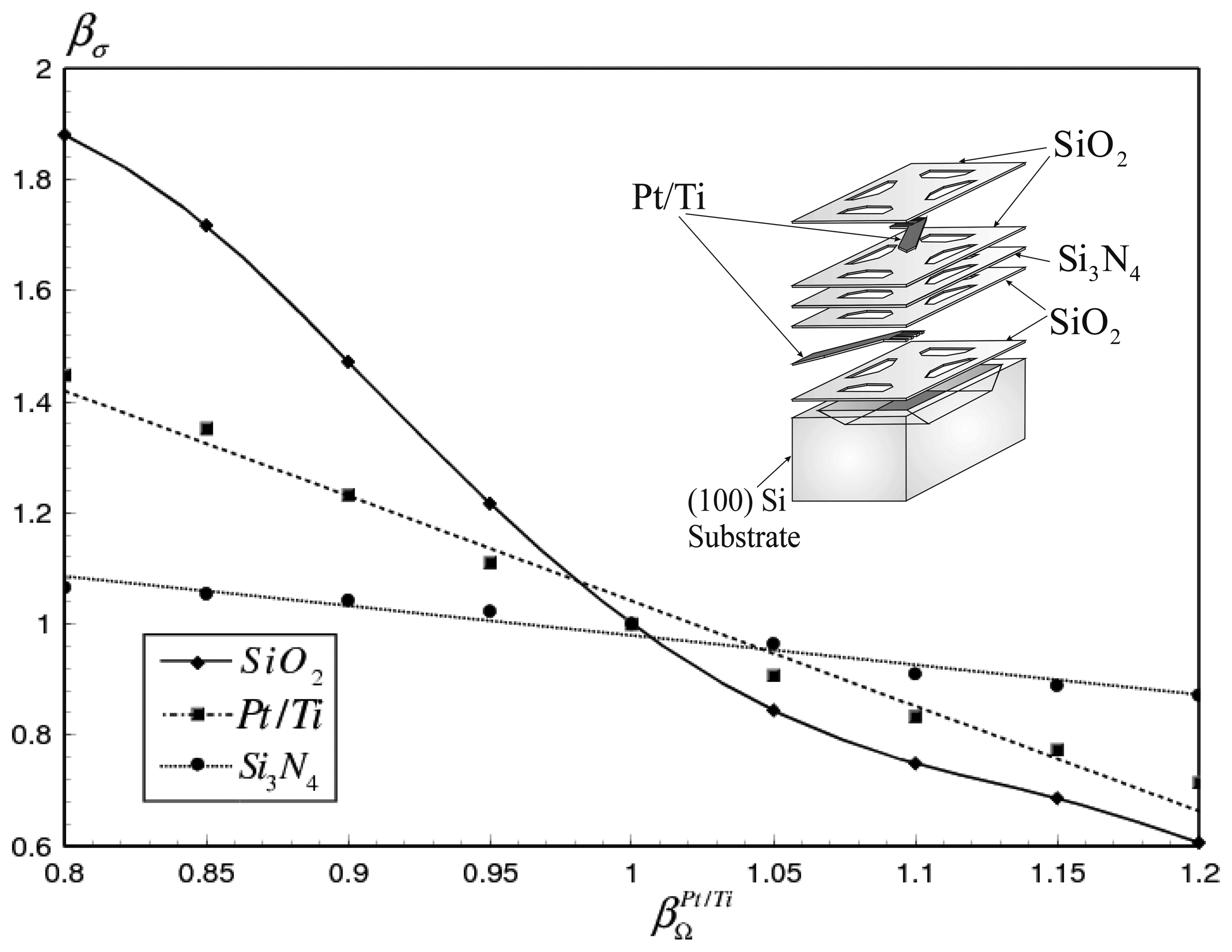
Figure 7.
Effect of electrical resistivity variation of polysilicon on the maximum thermal stress of different gas sensor materials
Figure 7.
Effect of electrical resistivity variation of polysilicon on the maximum thermal stress of different gas sensor materials
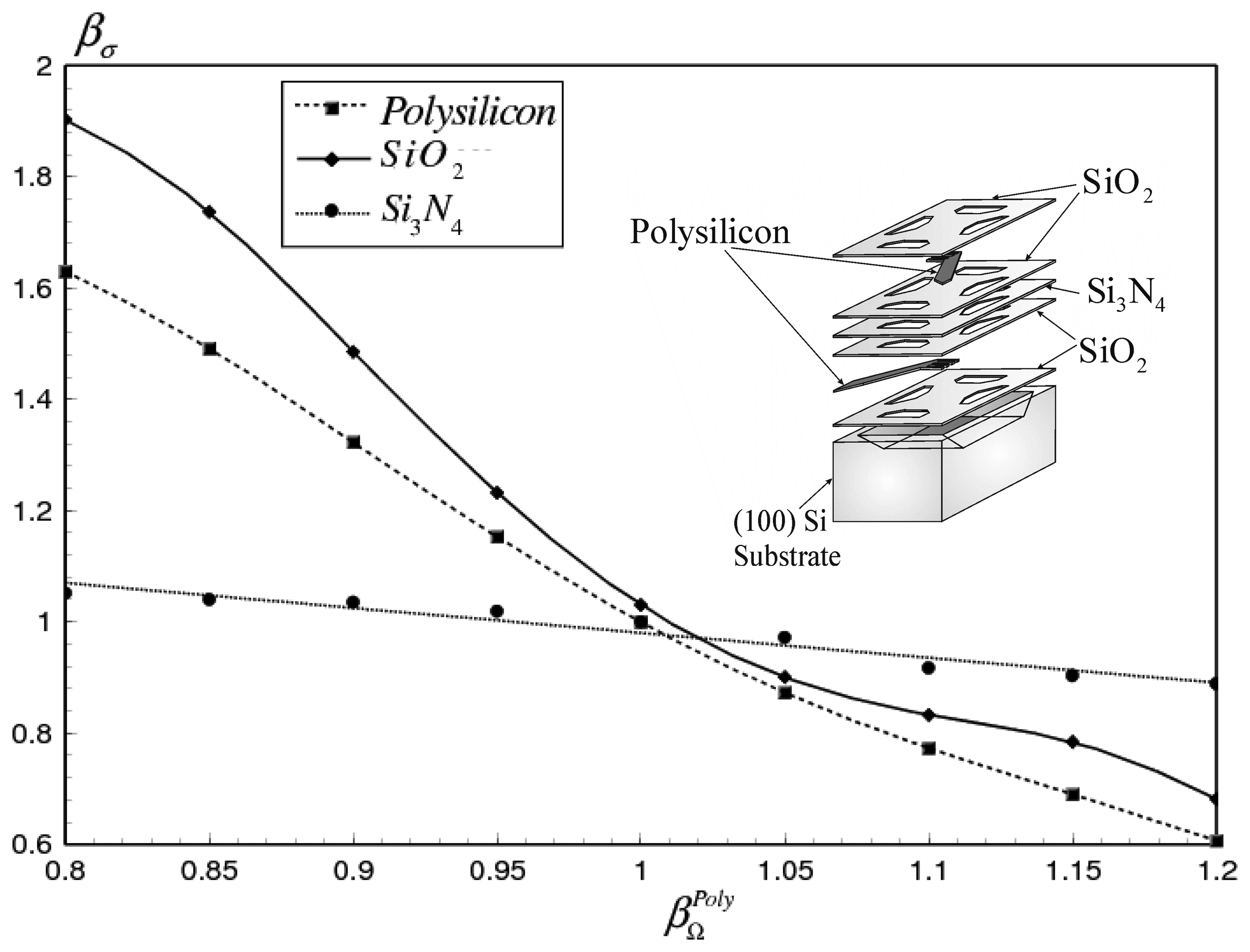
Figure 8.
Effect of the variation of the coefficient of thermal expansion of Si3N4 on the maximum thermal stress of different gas sensor materials
Figure 8.
Effect of the variation of the coefficient of thermal expansion of Si3N4 on the maximum thermal stress of different gas sensor materials

Figure 9.
Effect of the variation of the coefficient of thermal expansion of PtTi on the maximum thermal stress of different gas sensor materials
Figure 9.
Effect of the variation of the coefficient of thermal expansion of PtTi on the maximum thermal stress of different gas sensor materials

Figure 10.
Effect of the variation of the coefficient of thermal expansion of polysilicon on the maximum thermal stress of different gas sensor materials
Figure 10.
Effect of the variation of the coefficient of thermal expansion of polysilicon on the maximum thermal stress of different gas sensor materials

Figure 11.
Effect of the variation of the coefficient of thermal expansion of SiO2 on the maximum thermal stress of different gas sensor materials
Figure 11.
Effect of the variation of the coefficient of thermal expansion of SiO2 on the maximum thermal stress of different gas sensor materials

Figure 12.
Effect of the variation of Young's modulus on the maximum thermal stress of different gas sensor materials
Figure 12.
Effect of the variation of Young's modulus on the maximum thermal stress of different gas sensor materials

Figure 13.
Effect of the variation of the coefficient of thermal expansion and deposition residual stress for Si3N4 on the equivalent alternating stress of Si3N4
Figure 13.
Effect of the variation of the coefficient of thermal expansion and deposition residual stress for Si3N4 on the equivalent alternating stress of Si3N4
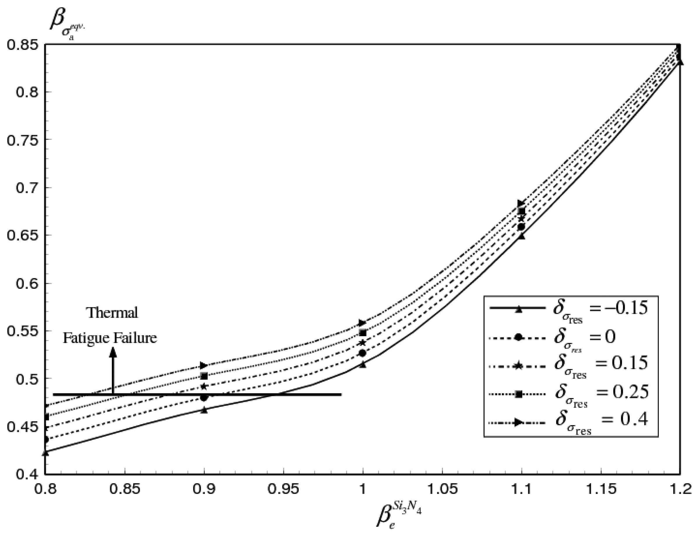
Figure 14.
Effect of the variation of the coefficient of thermal expansion and deposition residual stress for Si3N4 on the expected fatigue life of the gas sensor
Figure 14.
Effect of the variation of the coefficient of thermal expansion and deposition residual stress for Si3N4 on the expected fatigue life of the gas sensor
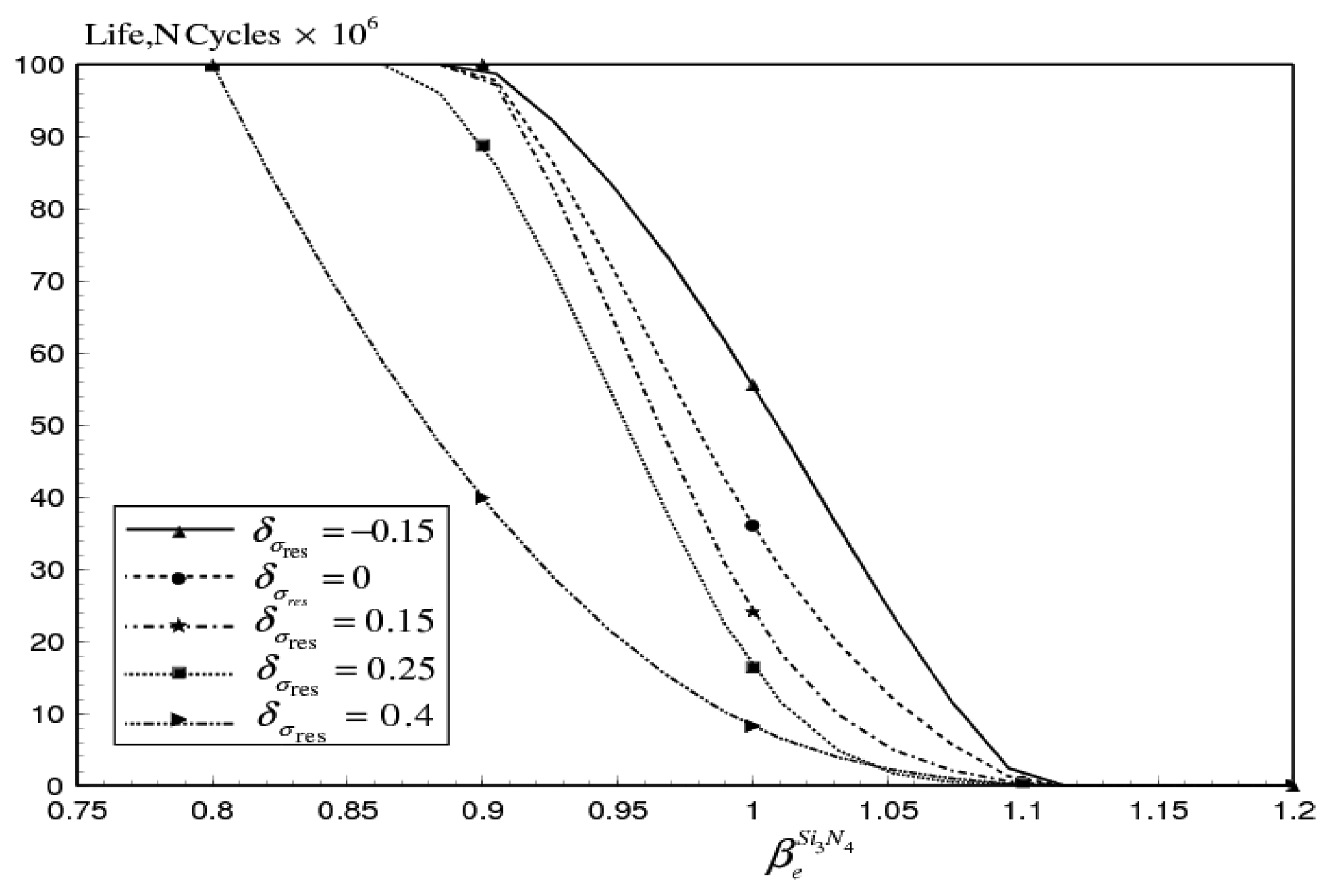
Figure 15.
Effect of the variation of Young's modulus and deposition residual stress for Si3N4 on the equivalent alternating stress of Si3N4
Figure 15.
Effect of the variation of Young's modulus and deposition residual stress for Si3N4 on the equivalent alternating stress of Si3N4
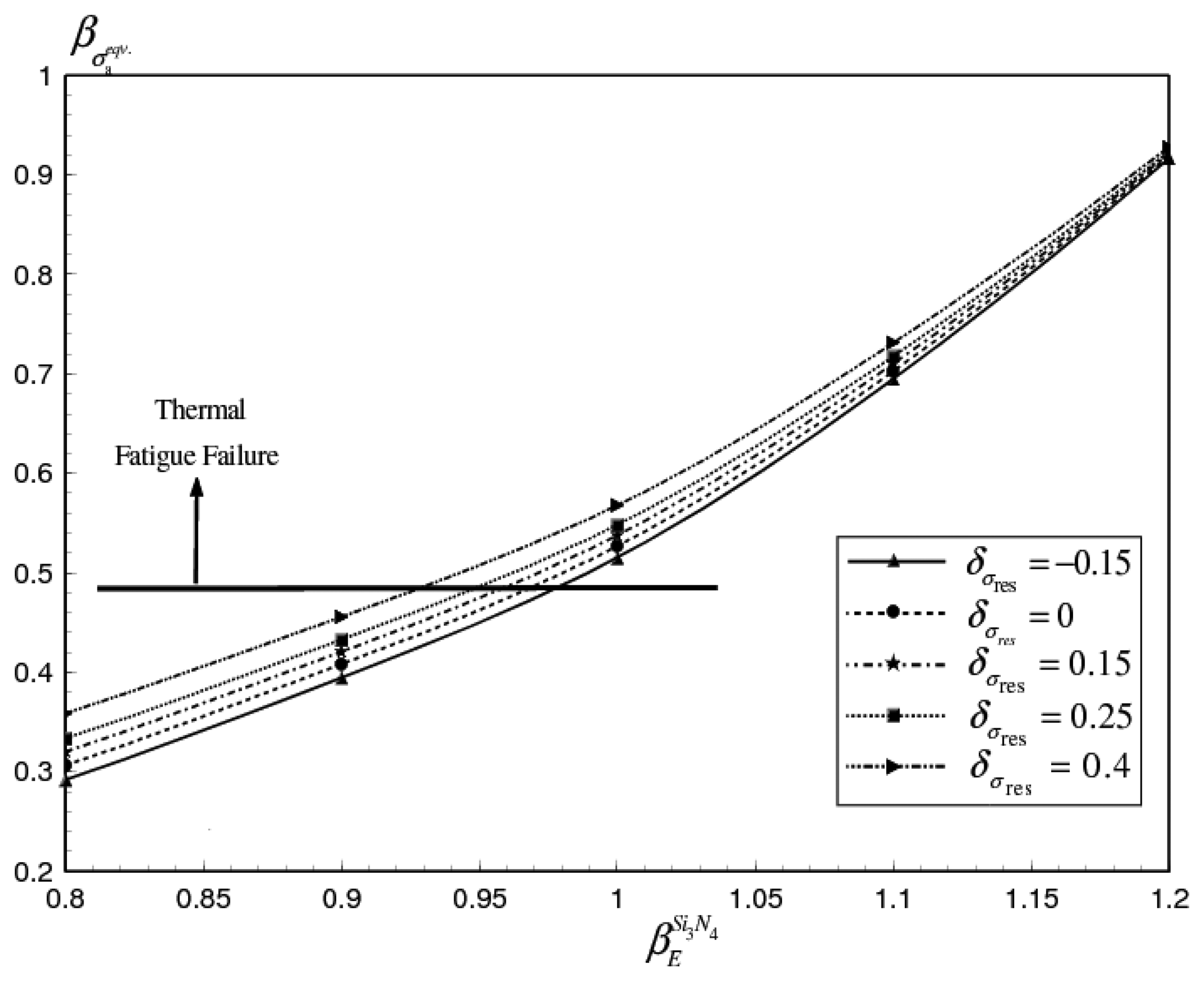
Figure 16.
Effect of the variation of Young's modulus and deposition residual stress for Si3N4 on the expected fatigue life of the gas sensor
Figure 16.
Effect of the variation of Young's modulus and deposition residual stress for Si3N4 on the expected fatigue life of the gas sensor

| Coefficient of Thermal expansion (α) (°C-1) | Young's Modulus (E) (GPa) | Residual Stresses (σres) (GPa) | Major Contributing Deposition Parameters | |
|---|---|---|---|---|
| SiO2 | 7×10⁻⁶ ±18% | 75 ± 7.8 | −0.3 → 0.3 | f (p,T) |
| Si3N4 | 3.3×10⁻⁶ ±18% | 310 ± 32 | −0.2 → 0.8 | f (T, G) |
| Pt/Ti | 0.97×10⁻⁵ ±18% | 140 ± 16 | 0.2 → 0.9 | f (DR) |
| Polysilicon | 2.7×10⁻⁶ ±18% | 162 ± 14 | −0.4 →0.3 | f (p,T) |
| σNmax (MPa) | σNmax/Sut | |
|---|---|---|
| SiO2 | 343 | < 0.3 |
| Si3N4 | 265 | ∼ 0.7 |
| Pt/Ti | 478 | ∼ 2 |
| Polysilicon | 341 | ∼0.08 |
| Equation | Material | ao | a1 | RMS |
|---|---|---|---|---|
| 2 | Si3N4 | 1.21 | -0.22 | 0.02 |
| 2 | Pt/Ti | 2.3 | -1.27 | 0.04 |
| 4 | Si3N4 | 1.51 | -0.53 | 0.02 |
| 4 | Pt/Ti | 2.93 | -1.90 | 0.05 |
| 6 | Si3N4 | 1.43 | -0.45 | 0.02 |
| 9 | Pt/Ti | -0.15 | 1.15 | 0.001 |
| 9 | Polysilicon | 0.78 | 0.23 | 0.001 |
| 9 | SiO2 | 0.62 | 0.38 | 0.005 |
| 10 | Si3N4 | -0.68 | 1.7 | 0.05 |
| 10 | SiO2 | -0.002 | 1.001 | 0.02 |
| 10 | Pt/Ti | -0.005 | 1.002 | 0.01 |
| Equation | Material | bo | b1 | b2 | b3 | b4 | RMS |
|---|---|---|---|---|---|---|---|
| 3 | SiO2 | -155.3 | -660 | -1019.5 | 690 | -172.4 | 0.02 |
| 3 | Polysilicon | -72.1 | 307.21 | -470.81 | 314.5 | -77.8 | 0.04 |
| 5 | SiO2 | -162 | 674.1 | -1020.4 | 674.9 | -165 | 0.001 |
| 7 | SiO2 | -199.2 | 833.6 | -1247.7 | 852.7 | -211.4 | 0.001 |
| 7 | Polysilicon | -59.3 | 254.24 | -386.8 | 255.1 | -62.2 | 0.001 |
| 8 | Si3N4 | -46 | 192 | -292.6 | 196.4 | -48.7 | 0.002 |
© 2007 by MDPI ( http://www.mdpi.org). Reproduction is permitted for noncommercial purposes.
Share and Cite
MDPI and ACS Style
Sadek, K.; Moussa, W. Studying the Effect of Deposition Conditions on the Performance and Reliability of MEMS Gas Sensors. Sensors 2007, 7, 319-340. https://doi.org/10.3390/s7030319
AMA Style
Sadek K, Moussa W. Studying the Effect of Deposition Conditions on the Performance and Reliability of MEMS Gas Sensors. Sensors. 2007; 7(3):319-340. https://doi.org/10.3390/s7030319
Chicago/Turabian StyleSadek, Khaled, and Walied Moussa. 2007. "Studying the Effect of Deposition Conditions on the Performance and Reliability of MEMS Gas Sensors" Sensors 7, no. 3: 319-340. https://doi.org/10.3390/s7030319