Modeling of Photoinduced Deformation in Silicon Microcantilever

ASIC and System National Key Lab, Department of Microelectronics, Fudan University, Shanghai 200433, China
*
Author to whom correspondence should be addressed.
Sensors 2007, 7(9), 1713-1719; https://doi.org/10.3390/s7091713
Submission received: 24 July 2007
/
Accepted: 27 August 2007
/
Published: 3 September 2007
(This article belongs to the Special Issue Cantilever, Microcantilevers and Nanocantilever Sensors and Biosensors)
Abstract
:A model for prediction the photostriction effect in silicon microcantilevers is built up based on the fundamentals of mechanics and semiconductor physics. By considering the spatial distribution and surface recombination of photoinduced carriers in silicon, the model interprets the cause of the photoinduced bending. The results from our model much more closely approximate the experimental values than the former model built up by Datskos, Rajic and Datskou [1](APL, Vol.73 (1998) No.16, pp 3219-2321), represented by the reduction of the error between calculation and measurement from 25 times to 0.85 times.
1. Introduction
The so called photostriction effect in semiconductors was found in germanium by Figielski in 1961 [2] and in silicon by Gauster and Habing six years later [3]. Similar effects were also found in some ceramic materials [4],and can be used as photostrictive actuators [5, 6]. Under that effect, the photogeneration of free charge carriers (electrons and holes) in a semiconductor, results in the development of a local mechanical strain [1, 7, 8]. In the late 1990s, Datskos's team investigated the photostriction effect in a silicon microcantilever structure [1, 7, 8]. It was also applied in photon detection [1, 7, 8] and chemical gas sensing [9]. They constructed a basic theory of the photostriction effect in a semiconductor cantilever structure. Their assumption was that the density of the photoinduced excess carriers was homogeneous in the microcantilever, shown by the average density they used to calculate photoinduced strain in equations 2 and 3 in reference [1, 7, 8]. However, their theoretical results were about 25 times larger than the experimental values [1, 7, 8]. In this study, by considering the spatial distribution and surface recombination of photoinduced carriers in silicon, we have constructed a model for prediction the photoinduced deformation in a microcantilever structure. The calculated results are also compared with Datskos's theoretical and experimental data.
2. Modeling
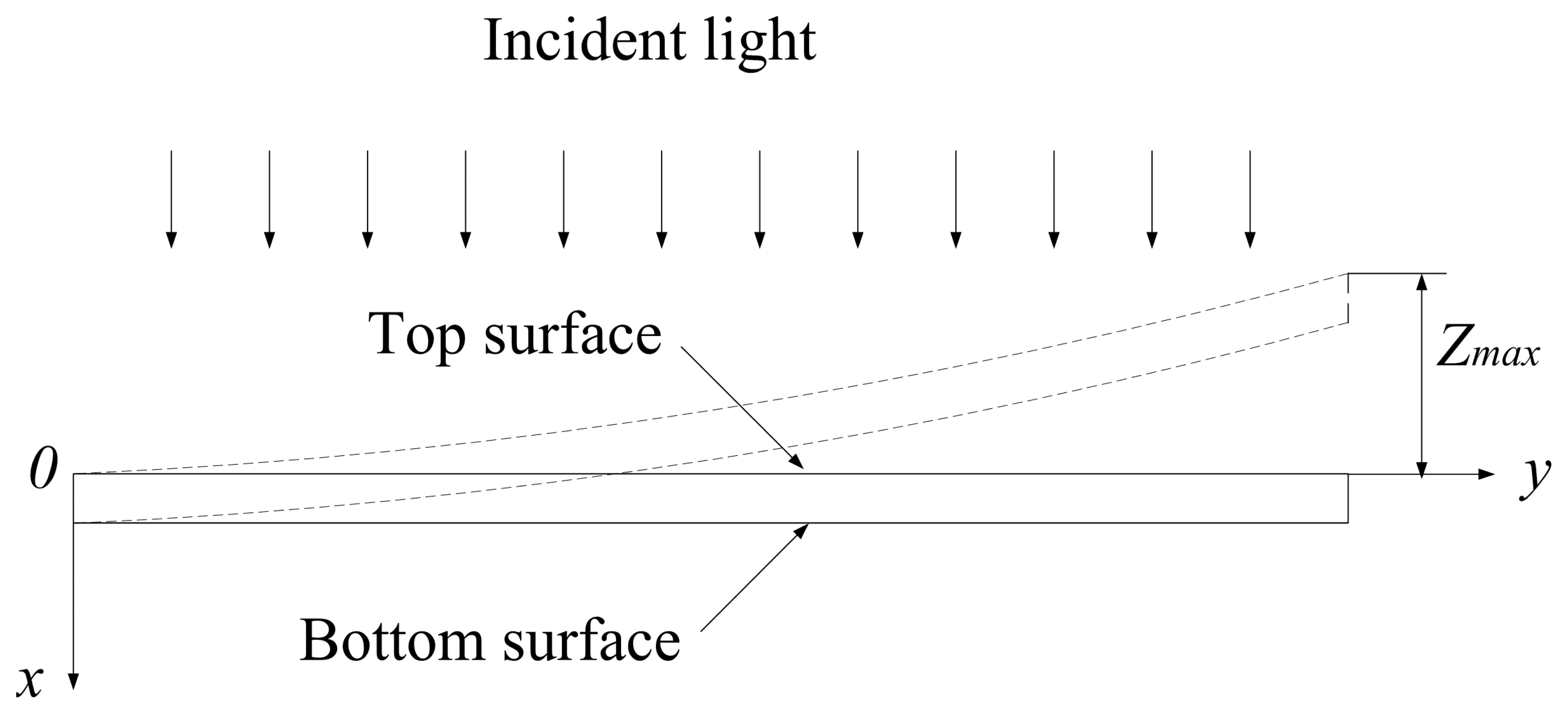
Under illumination with light with an energy above the band gap of silicon, the lattice in the microcantilever will be strained as the presence of excess electron-hole-pairs. Different from Datskos's assumption of homogeneous excess carriers, we suppose that the light intensity will be reduced along the depth of the cantilever (x direction in Figure 1), because of the intensive absorption of photons by Si. Therefore, the density gradient of the excess carries causes a strain gradient in the cantilever and thus the bending of the silicon cantilever.
Assuming that the light intensity at the top surface of the microcantilever is a constant, I0, the light intensity I along the x direction is as expressed by [10]:
where α is light absorption coefficient of silicon.
Following Datskos's deduction, the density of photoinduced excess carriers is given by [10]:
where η is the quantum efficiency and τ is the life time of the excess carriers in silicon.
The photoinduced strain is given by
where β is the photostriction coefficient. [2]
Derived from equations (1-3), the relationship between the light and the photoinduced strain can be written as:
For a cantilever with a rectangular cross section, the deformation curvature of the structure can be given by [11]
where W, H, and I are the width, thickness and the moment of inertia of the microcantilever, respectively. E is the elastic modulus of the cantilever, given by Ey/(1− υ) with the Poisson's ratio of silicon υ. M is the bending moment, which is the integral force moment of the forces (against the neutral plane) across the cross section of the structure [11], given by
In order to compare with Datskos's expression in reference [1, 7, 8], the above equation can be rewritten as
where a = 1 − e−αH, which is the photo absorptivity of silicon [10]. Let
Two obvious differences between the two equations can be seen. One is that in our equation, there is a' but not a as in Datskos's equation. In Equation (10), the first item 2-a indicates the effect of the photo absorptivity a on the part of the microcantilever above the neutral plane, while the second item
indicates the effect of the photo absorptivity a on the part below the neutral plane. a' and a denote two different strain generation mechanisms, i.e., the density of photoinduced excess carriers in the cantilever is asymmetrical in our theory while homogenous in Datskos's. The other is that in our Eq. (9), there is no item including the Poisson's ratio as in Datskos's equation. The reason is that because photostriction effect directly results in local mechanical strain. That indicates the photo-induced bending is caused by lattice contraction, not by stress. Therefore, the elastic modulus of the cantilever is eliminated from the deformation equation.
Furthermore, the recombination of the photoinduced excess carriers at the top and bottom surfaces must be considered in the prediction of the deformation, because the thickness of the microcantilever is as thin as some hundreds nanometers (e.g. 500 nm in [1]). The recombination of the photoinduced excess carriers has a great effect on the carrier density and thereafter the photoinduced strain. In addition, the surface recombination velocity is different at the two surfaces, which also plays an important role in the photoinduced bending. From the viewpoint of fabrication, one of the two surfaces of the microcantilever is formed by etching with rough surface, and the other is formed by the original polished silicon surface. The surface recombination velocity at the rough surface is much faster than that at the polished surface.
Suppose that excess carrier density at the etched surface equals to 0, while the carrier recombination at the polished surface can be omitted. Under this assumption, the bending moment M and deflection Zmax can be approximated as follows.
3. Verification of the model
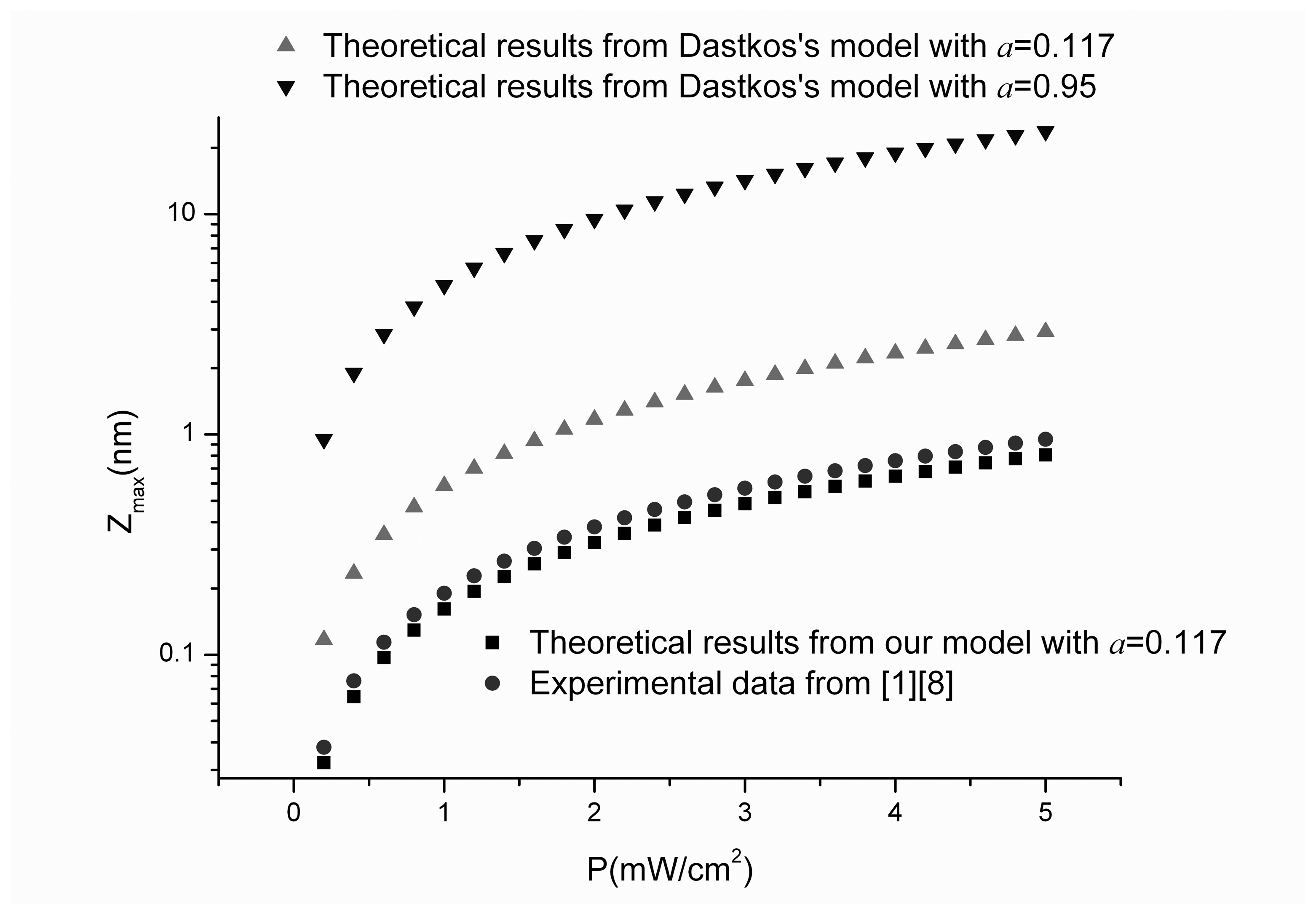
To verify our model, the calculated results from our model are compared with the theoretical and experimental data in [1, 8]. The experimental parameters are listed in Table 1. It should be noted that the photo absorptivity of silicon was set as a=0.95 in [1, 8], which is about ten time larger than its real value. From [12], for λ=780nm, a can be derived as 0.0952-0.1393 with the light absorption coefficient of silicon in the range of 2×10³ to 3×103cm-1. In our calculation, we set a as the average value of 0.117. The results shown in Figure 2 are the calculated data by Datskos's model (Eq. 11) and our model (Eq. 13), in addition with Datskos's experimental data in [1, 8]. The experimental data in Figure 2 is obtained from the fitting line shown in [1, 8].
The x ordinate of the plot is power density P instead of absorbed power Φ used in [1, 8] because we have to put theoretical data with a=0.95 and a=0.117 both in the plot for comparison. Power density P is given by P=I0hC/λ, where h is Planck's constant and C is the velocity of light. The y ordinate shows the maximum deflection on a logarithmic scale.
From the figure, higher accuracy of our model is obvious. For a=0.117, our theoretical data is 0.85 times the experimental one, while the results from Datskos's model are about 25 times when a=0.95 and 3 times when a=0.117 larger than that they measured. The difference between our calculation and the experimental data most likely comes from the assumption on the carrier recombination velocity of the top and bottom surfaces of the microcantilever.
4. Conclusions
In summary, we have introduced a model to calculate the photoinduced bending of a Si microcantilever, based on the theory of the gradient of photoinduced excess carrier and the carrier recombination at the two surfaces of the microcantilever. The result from our model is 0.85 times that of the measurement, which is much more accurate than the results from the former model. It has been revealed that the photoinduced bending is induced by the gradient of photoinduced excess carrier and the different recombination velocity between top and bottom surface on the cantilever.
Acknowledgments
This research work is supported by the Natural Science Foundation of China under Grant No. 60476032, and by the Open Research Fund of the Key Laboratory of MEMS of Ministry of Education, Southeast University.
References
- Datskos, P.G.; RaJic, S.; Datskou, I. Photoinduced and thermal stress in silicon microcantilevers. APPLIED PHYSICS LETTERS 1998, 73, 2319–2321. [Google Scholar]
- Figielski, T. Photostriction Effect in Germanium. Phys. Status Solidi (b) 1961, 1, 306–316. [Google Scholar]
- Poosanaas, P.; Uchino, K. Photostrictive effect in lanthanum-modified lead zirconate titanate ceramics near the morphotropic phase boundary. Materials Chemistry and Physics 1999, 61, 36–41. [Google Scholar]
- Poosanaas, P.; Tonooka, K.; Uchino, K. Photostrictive actuators. Mechatronics 2000, 10, 467–487. [Google Scholar]
- Sun, D.; Tong, L. Modeling of wireless remote shape control for beams using nonlinear photostrictive actuators. International Journal of Solids and Structures 2007, 44(2), 672–684. [Google Scholar]
- Gauster, W.B.; Habing, D.H. Electronic Volume Effect in Silicon. Physical Review Letters 1967, 18, 1058–1061. [Google Scholar]
- Datskos, P.G.; Rajic, S.; Egert, C.M.; Datskou, I. Detection of infrared photons using the electronic stress in metal-semiconductor interfaces. Part of the SPIE Conference on Infrared Technology and Applications XXV 1999, SPIE. 3698, 151–160. [Google Scholar]
- Datskos, P.G.; Rajic, S.; Datskou, I.; Egert, C.M. Novel photon detection based on electronically induced stress in silicon. Part of the SPIE Conference on Infrared Detectors and Focal Plane Arrays V 1998, SPIE. 3379, 173–181. [Google Scholar]
- Datskos, P.G.; Rajic, S.; Sepaniak, M.J.; Lavrik, N.; Tipple, C.A.; Senesac, L.R.; Datskou, I. Chemical detection based on adsorption-induced and photoinduced stresses in microelectromechanical systems devices. J.Vac.Sci.Technol. B 2001, 19, 1173–1179. [Google Scholar]
- Liu, E.; Zhu, B.M.; Luo, J. Semiconductor Physics, 6th Edition ed; Publishing House of Electronics Industry: Beijing, 2003; p. 323. [Google Scholar]
- Bao, M. Analysis and Design Principles of MEMS Devices; ELSEVIER: Amsterdam, 2005; p. 46. [Google Scholar]
- Sze, S.M. Physics of Semiconductor Devices, 2nd Edition ed; John Wiley & Sons: New York, 1981; pp. 41–44. [Google Scholar]
Figure 1.
Schematic of a Si microcantilever under incident light and the coordinate system

© 2007 by MDPI ( http://www.mdpi.org). Reproduction is permitted for noncommercial purposes.
Share and Cite
MDPI and ACS Style
Guo, Y.-L.; Zhou, J.; Huang, Y.; Bao, M. Modeling of Photoinduced Deformation in Silicon Microcantilever. Sensors 2007, 7, 1713-1719. https://doi.org/10.3390/s7091713
AMA Style
Guo Y-L, Zhou J, Huang Y, Bao M. Modeling of Photoinduced Deformation in Silicon Microcantilever. Sensors. 2007; 7(9):1713-1719. https://doi.org/10.3390/s7091713
Chicago/Turabian StyleGuo, Yu-Lin, Jia Zhou, Yiping Huang, and MinHang Bao. 2007. "Modeling of Photoinduced Deformation in Silicon Microcantilever" Sensors 7, no. 9: 1713-1719. https://doi.org/10.3390/s7091713