Multi-scale Analysis of MEMS Sensors Subject to Drop Impacts


1
Dipartimento di Ingegneria Strutturale, Politecnico di Milano, Piazza L. da Vinci 32, 20133 Milano (Italy)
2
MEMS Product Division, STMicroelectronics, Via Tolomeo 1, 20010 Cornaredo (Italy)
*
Author to whom correspondence should be addressed.
Sensors 2007, 7(9), 1817-1833; https://doi.org/10.3390/s7081817
Submission received: 30 August 2007
/
Accepted: 6 September 2007
/
Published: 7 September 2007
(This article belongs to the Special Issue Modeling, Testing and Reliability Issues in MEMS Engineering)
Abstract
:The effect of accidental drops on MEMS sensors are examined within the framework of a multi-scale finite element approach. With specific reference to a polysilicon MEMS accelerometer supported by a naked die, the analysis is decoupled into macro-scale (at die length-scale) and meso-scale (at MEMS length-scale) simulations, accounting for the very small inertial contribution of the sensor to the overall dynamics of the device. Macro-scale analyses are adopted to get insights into the link between shock waves caused by the impact against a target surface and propagating inside the die, and the displacement/acceleration histories at the MEMS anchor points. Meso-scale analyses are adopted to detect the most stressed details of the sensor and to assess whether the impact can lead to possible localized failures. Numerical results show that the acceleration at sensor anchors cannot be considered an objective indicator for drop severity. Instead, accurate analyses at sensor level are necessary to establish how MEMS can fail because of drops.
1. Introduction
Inertial micro-electromechanical sensors can sometimes fail because of incorrect handling or accidental drops. An accurate modeling of failures caused by such events can help the management and design of MEMS transport and working condition.
Recently, some researches have studied how the effects of drops or impacts can be dealt with by a reliability analysis of inertial MEMS sensors (see, e.g., [1–3]). Almost all these works proposed simplified models to link drop features with the stress state in the MEMS. The details of shock waves propagating inside the package and/or the die after impact against a target surface, can not be appropriately captured by these reduced order models: a rather low accuracy is therefore achieved when localized sensor failures are of concern [3].
To improve accuracy, a multi-scale finite element procedure is here proposed and adopted to study a uni-axial polysilicon MEMS accelerometer supported by a naked die and subject to accidental drops. The influence of falling orientation and the interaction between sensor and die/cap are investigated. A trial in this direction has been already proposed in [3], where detailed numerical simulations at the sensor level were run to define, according to a statistical failure analysis, the probability of rupture of MEMS accelerometers after impacts. In the present work, which has to be meant as a first step towards the construction of a fully coupled multi-scale numerical procedure, we start assessing the effects of drops and, more generally, of impacts at the die (macroscopic) and sensor (mesoscopic) length scales. Within the offered frame, micro-scale analyses for polycrystalline sensors should have to account for the nonlinear phenomena occurring at the crystal length scale like, e.g., crack nucleation and propagation, bulk damping and plasticity. Here we a-priori assume that in case of impacts a major role is played by the propagation of cracks at grain boundaries and within grains [4]. Since polysilicon is brittle at room temperature [5], a local rupture can occur when the stress field satisfies a stress-based failure criterion. We therefore avoid running micro-scale simulations; instead, an experimentally determined tensile strength of the polysilicon is required.
Since MEMS are characterized by a mass smaller by several orders of magnitude than the die or the package ones, the dynamics of the whole device after impacts is only marginally affected by the presence of the MEMS itself. A decoupling between macro-scale (at die level) and meso-scale (at MEMS level) simulations is thus allowed. Following a standard top-down approach, in macro-scale analyses the whole device is modeled while falling and bouncing off a target surface; the effects of the shape of the die, of the drop height and of the falling orientation on the displacement/acceleration history and, specially, on the acceleration peaks at the sensor anchors can be established. In meso-scale analyses the displacement evolution at the anchor points are adopted as loading conditions for the sensor; critical MEMS details, where the stress state can exceed the polysilicon carrying capacity, can thus be identified.
In all the analyses we assume the MEMS to behave elastically. This constitutive assumption prevents an accurate simulation of the failure mode, i.e. of how the MEMS eventually brakes. In what follows, according to the above mentioned strength criterion for brittle materials, we aim at detecting if and where the local stress field approaches or even exceeds the tensile strength of the polysilicon; we are therefore mainly collecting information on the drop conditions leading to failure of a MEMS component. In case a detailed description of the failure process is in need, micro-scale analyses accounting for the actual crystal structure of the polysilicon must be adopted [6–8].
To define drop severity, the acceleration peak felt by the MEMS, estimated according to an enhanced Hertz theory accounting for dynamic effects [9], is usually adopted for micro-systems. The main out-come of our simulations is that the said estimation can not lead to an objective classification of drop severity. In fact, the Hertz theory provides acceleration peaks different by orders of magnitude from those furnished by the finite element approach, and can not distinguish among the possible falling orientations. Furthermore, it is shown that drops leading to higher acceleration peaks are not necessarily the worst ones in terms of failure probability; some stress fields turn out to be more severe than others, even if associated to lower acceleration peaks. This depends on how the MEMS interacts with the surfaces of the die/cap while vibrating after the impact. According to what already envisaged in [10], the proposed multi-scale scheme can be adopted to detect failures caused by device drops.
2. Mechanical properties of polysilicon films
When the size of a structural component is comparable with the silicon grain size (typically 0.2 – 0.7 μm), the hypothesis of homogeneous bodies is no longer applicable [5, 6, 11, 12]. This occurs in the studied devices at the micro-scale, i.e. at the scale of the accelerometer details. However, since the aim of this work is to detect the most critical drop configurations and not to investigate the relevant failure mechanism, an homogenized transversely isotropic constitutive model is adopted for the polysilicon at the sensor level. As shown in [12], results are expected to be significant if the MEMS or its details are constituted by at least a few hundreds of grains.
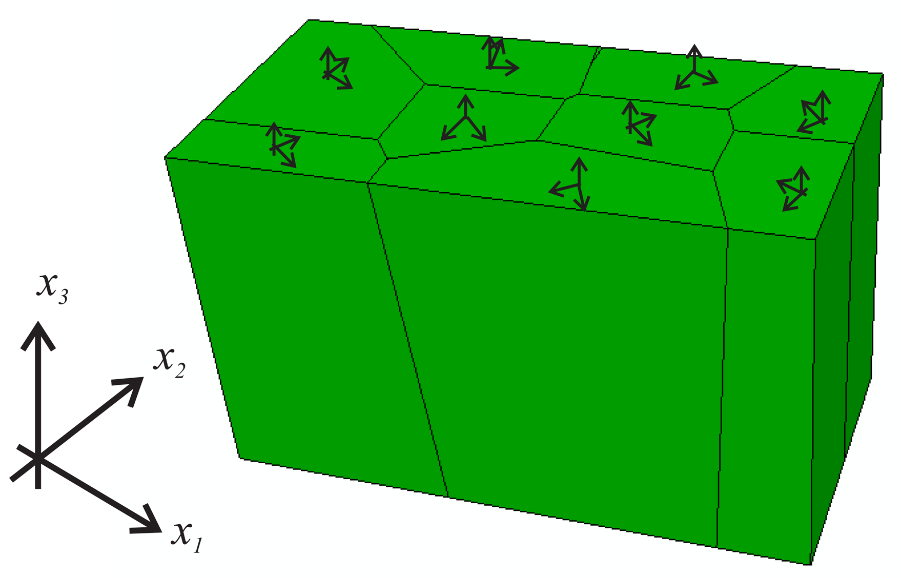
The polycrystalline silicon here studied has a columnar structure, being obtained via epitaxial growth from a flat substrate. Furthermore, the texture axis can be assumed coincident with axis x3 (see Figure 1), i.e. perpendicular to the substrate surface.
Adopting a standard Voigt notation for solid mechanics [13], the matrix S of elastic moduli (linking the stress vector σ to the strain vector ε through σ = Sε) for single-crystal silicon can be expressed as follows:
where [14 – 16]: s11 = 165.7 GPa, s12 = 63.9 GPa, s44 = 79.6 GPa.
As shown in the sketch of Figure 1, grains have a privileged direction aligned with axis x3 but a random orientation of the other two axes of elastic symmetry in the x1 – x2 plane. The overall response of the crystal assembly, to be adopted in meso-scale analyses, can hence be assumed transversely isotropic, the axis of transverse isotropy being coincident with axis x3. In the relevant homogenized matrix S of elastic moduli five independent parameters appear: the in-plane (namely in the x1 – x2 plane) Young's modulus E and Poisson's ratio v; the out-of-plane (namely along axis x3) Young's modulus Ē; the shear modulus Ḡ and the Poisson's ratio v̄ linking in-plane and out-of-plane deformation components. According to the crystal structure described above, constants Ē, v̄, Ḡ are assumed coincident with the single crystal ones, i.e. Ē = 130.10 GPa, Ḡ = 79.6 GPa, v̄ = 0.28; on the other hand, in-plane moduli E and v are bounded as described here below.
Due to the random orientation of the in-plane privileged directions of the grains, an iso-strain (Voigt-like) bound on matrix S is furnished by [15]:
where T stands for transpose and Te is the orthogonal transformation matrix that defines the variation of the strain vector components while passing from the local privileged crystal reference frame to the overall one, aligned with axes xi ,i= 1,2,3.
Following a similar approach, an iso-stress (Reuss-like) bound on S is given by [15]:
where Tσ plays the same role of Tε when defining the variation of the stress vector components.
Each silicon grain displays a fcc material symmetry, with a small anisotropy level (see [15]); the bounds on E and v are thus expected to be tight. In fact, it turns out that the homogenized in-plane Young's modulus is bounded by Eσ = 147.1 GPa and Eε = 158.7 GPa, while the in-plane Poisson's ratio is bounded by vε = 0.18, vσ = 0.22. Due to relatively small difference between the two bounds, henceforth we assume as in-plane elastic moduli the mean value of the two bounds, i.e. E = 152.9 GPa and v = 0.2.
3. Multi-scale analysis of inertial polysilicon MEMS: preliminaries
A multi-scale finite element approach is here used to get insights into the drop features leading to possible sensor failure. A decoupling among the length-scales is allowed by the very small ratio between the masses of the sensor and of the whole die/cap assembly (or of the whole package). Since the behavior of the polysilicon is assumed elastic up to failure, results are not expected to provide a detailed description of the possible failure mechanism(s); whereas, sites where the stress state exceeds the material tensile strength can be clearly identified.
In the analyses to follow, a few simplifying hypotheses are introduced:
- -
- air viscosity during drop is neglected;
- -
- the impacted (target) surface is assumed flat and rigid;
- -
- contact between the device and the target surface is frictionless;
- -
- fluid-sensor interaction, leading to viscous damping, is neglected.
The above assumptions are commonly expected to give rise to an overestimation of the stress field; therefore, the sensor carrying capacity against shock loadings is underestimated.
As far as the mentioned tensile strength of the polysilicon is concerned, a final remark is in need. For heterogeneous materials the strength is a local feature that continuously varies inside the body; this variation can be particularly remarkable in brittle materials, which are more sensitive to internal defects. Mainly because of the variation of the crystal structure, the strength of the polysilicon varies unpredictably from specimen to specimen, even when nominally identical geometries and loading conditions are considered [17]. To handle such kind of problems, a non deterministic (statistical) approach based on Weibull theory [18] is here adopted, see e.g. [19]. According to data furnished by the sensor supplier, the reference tensile strength is assumed σ0 ≈ 4 GPa; this value corresponds to a failure probability of 63.2% for a sample under uniaxial tensile loading conditions. This reference value σ0 is then deter-ministically compared to the local stress field envelopes in order to assess if and where the MEMS can fail.
4. Simulation of MEMS failure caused by accidental drops
After a frictionless impact against a flat target surface, the falling die repeatedly bounces. Customarily, the severity of the drop is estimated through the acceleration peak felt by the sensor. However, as already pointed out in [1] for much simpler structures, this information can not always be objective if the resistance of MEMS to shock loading is under study.
If the die is approximated as a compact, spherical-like body with characteristic radius R, made of an isotropic elastic material with Young's modulus Ed and Poisson's ratio vd, and the target is assumed perfectly flat and made of an isotropic elastic material with Young's modulus Et and Poisson's ratio vt, then an analytical estimate ā of the said acceleration peak felt by the sensor is given by [9]:
vimp being the velocity of the die while impacting the target surface, and m its mass. The analyses are here aimed at modeling accidental drops mainly due to mis-handling; hence, drop height has been assigned as h=150 cm. For the studied device, in case of impacts against a rigid target, the reference acceleration ā turns out to be on the order of 105 g, g = 9.81 m/s2 being the gravity acceleration.
4.1. Macro-scale analysis
In the present numerical scheme, at this length-scale the propagation of shock waves in the bulk of the falling die/cap assembly is explored. Three-dimensional dynamic simulations are run to capture the response of the whole body during and after the impact.
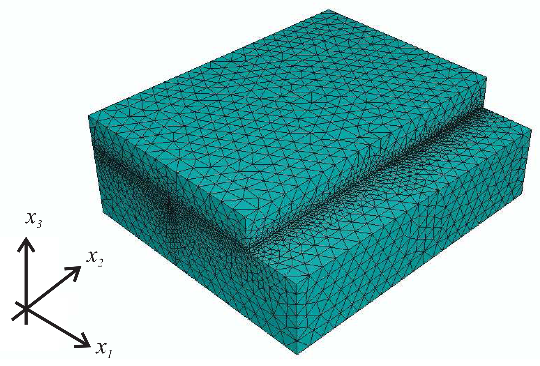
The geometry of the modelled device is shown in Figure 2: a space discretization consisting of about 145,000 tetrahedral, 4-node linear elements and about 30,000 nodes has been adopted.
Both die and cap are made of single-crystal silicon. Since shock waves do not lead to appreciable dissipative phenomena at this scale, silicon is assumed elastic. Furthermore, because of the small anisotropy level of the silicon (see Section 2), the body is assumed to be isotropic, with Young's modulus Ed =130 GPa, Poisson's ratio vd =0.22 and mass density ρd = 2330 Kg/m3.
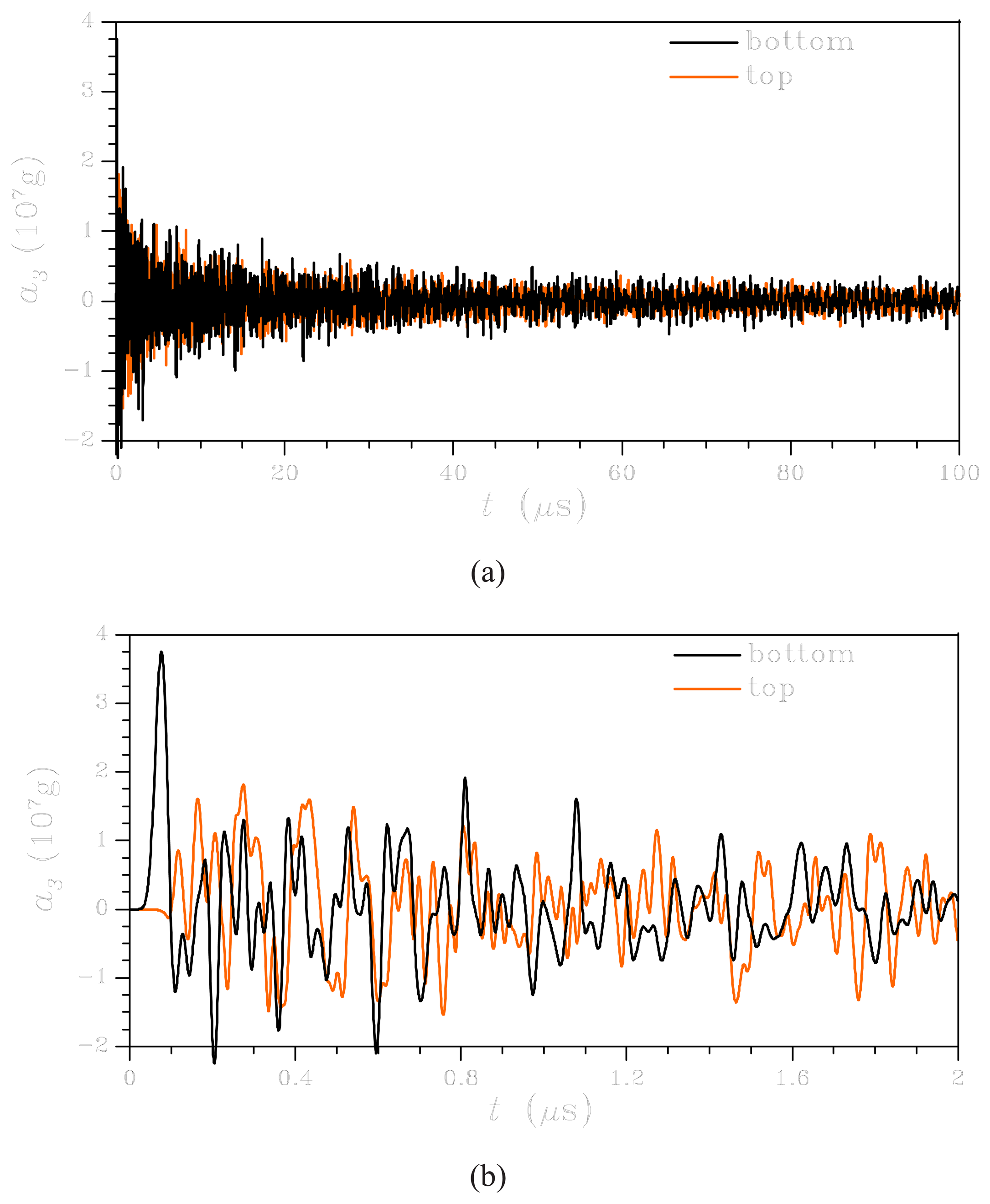
Because the cap is asymmetrically positioned with respect to the center of gravity of the whole die/cap assembly (see Figure 2), while falling and bouncing the assembly is affected by a rotation around axis x2. To account for the effects of this tilting, two different collisions with the target surface have been explored, see Figure 3: in the first one (bottom case) the die strikes the target surface with its bottom surface; in the second one (top case) the die strikes the target surface up-side down, leading to a contact with the upper surface of the cap. According to symmetry, tilting around axis x1 has been prevented.
Interactions between the shock waves emanating from the surface that strikes the target takes place inside the die; all the simulations last 100 μs which can be shown to be a reasonable bound on the time interval to be scanned to detect peak stress states in the sensor.
During the analyses, the acceleration at the sensor anchor(s) is continuously monitored. Because of the above described asymmetric geometry of the die-cap assembly, rigid body-like rotations of the assembly itself show up after the impact, specially for t > 50 μs (t being time); therefore, also the rotational acceleration at the sensor anchor(s) is stored.
Figure 4 shows a comparison between the acceleration records in the sensing direction x3 (see Figure 2) caused by top and bottom drops, in the interval 0 < t < 100 μs; to highlight the sequence and the magnitude of the peaks, a detail of the records just after the impact, namely for 0 < t < 2 μs, is also depicted. Due to the multiple reflections of the shock waves at the free surfaces of the device, a large amount of peaks show up. The highest peaks are anyway located in short time intervals after the impacts, whereas oscillations appear to be damped for t > 40 μs. By comparing these graphs with the values furnished by Eq. (4), it can be noticed that the analytical estimate fails because of two reasons: it is not able to distinguish between top and bottom drops, namely it is not able to determine which impact configuration is the worst one (obviously, in terms of the highest acceleration peak); it underestimates the acceleration peaks by two orders of magnitude.
Hence, it can be finally claimed that Eq. (4) has to be interpreted at best as a rough estimate of the maximum acceleration peak that the sensor anchor experiences after the impact with a rigid target. This is due to the fact that theory leading to (4) has been developed to furnish the acceleration of the center of mass of the falling body, while it lacks the capability to describe local effects due to the propagation of shock waves.
4.2. Meso-scale analysis
At this length-scale the response of MEMS to shock loadings is simulated. The main goal of the analyses is to detect where the stress state caused by the drop approaches or even exceeds the tensile strength of the polysilicon.
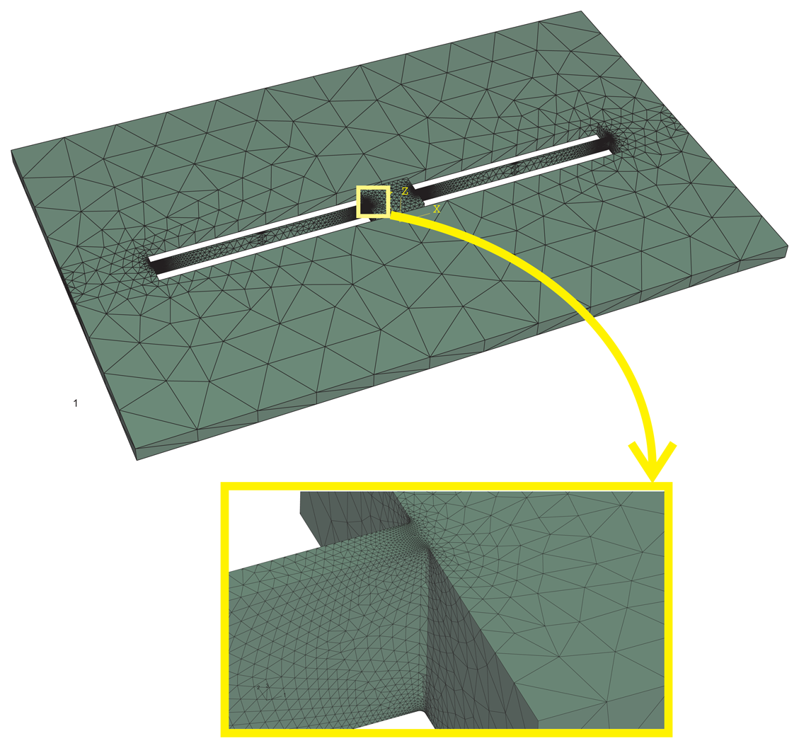
The sensor under study is depicted in Figure 5; it is constituted by a seismic mass (or massive plate), connected via two slender beams (or springs) to the anchor point. Both the seismic plate and the beams are made of polycrystalline silicon, whose material properties have been given in Section 2. To assess how the MEMS interacts with the die during the vibrations that follow the impact, the results of two series of simulations are compared next: in the first one the possible interactions of the movable parts of the sensor (plate and springs) with stoppers and with top/bottom surfaces of the cavity inside the die/cap assembly are disregarded; in the second one the said interactions are fully accounted for.
To this purpose, the sensor has been discretized with about 77,500 tetrahedal 4-node elements, while die/cap and stopper surfaces have been assumed rigid. Loading conditions are defined through motion at the anchor, according to the displacement record obtained in the macro-scale analyses at the same anchor point.
Because of the sensor lay-out, bending vibrations of the plate turn out to be negligible; on the other hand the springs, due to their slender geometry, are subject to coupled bending-torsional vibrations. Re-entrant corners at the end of the springs give rise to an amplification of the stress field in the surrounding region: the details which are prone to failure can therefore be identified as the spring-anchor and the spring-plate joint sections. A detailed resolution of the stress state in these regions is necessary to accurately capture the drop features leading to sensor failure: this requirement motivates the adopted mesh shown in the detail of Figure 5.
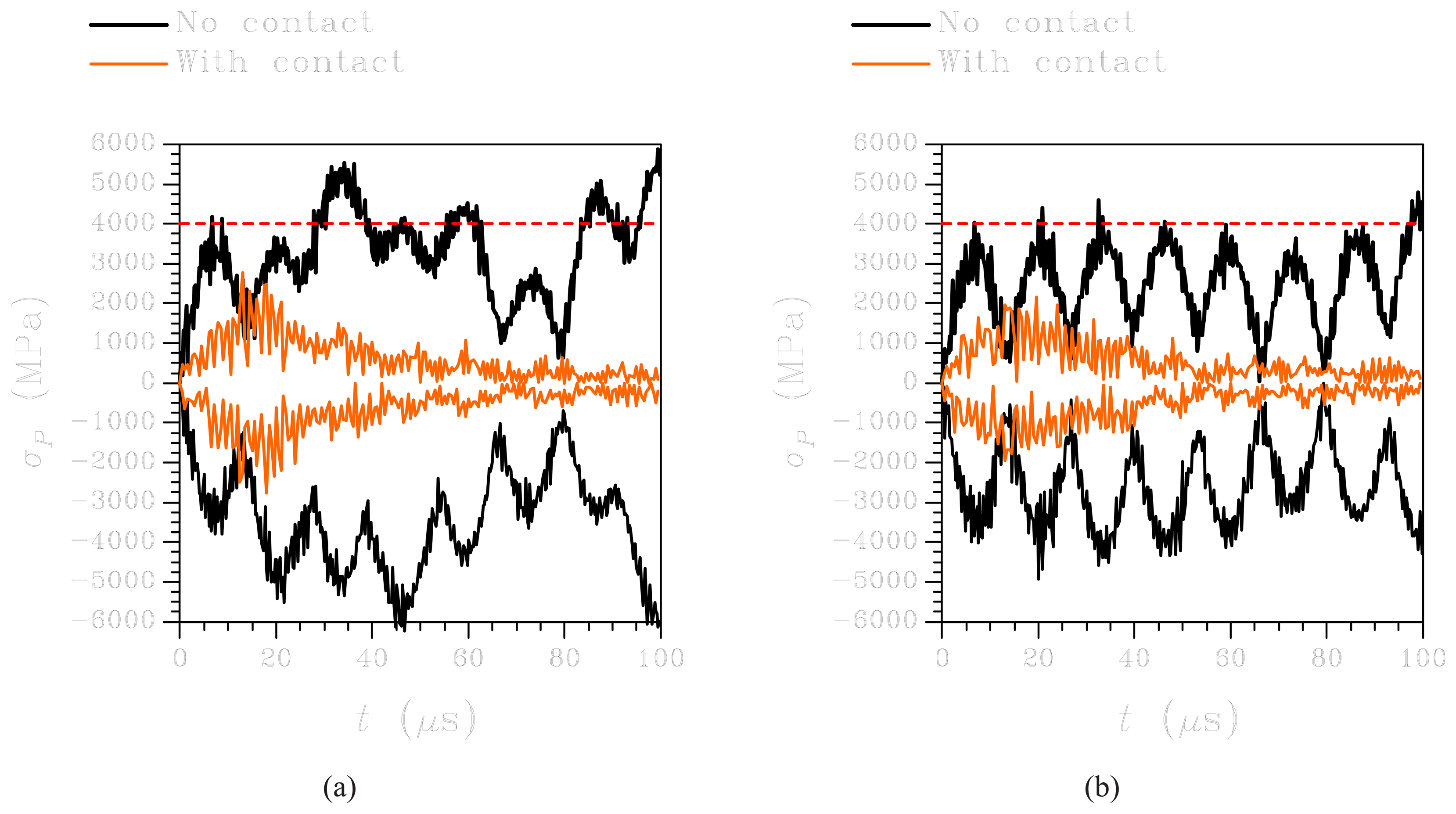
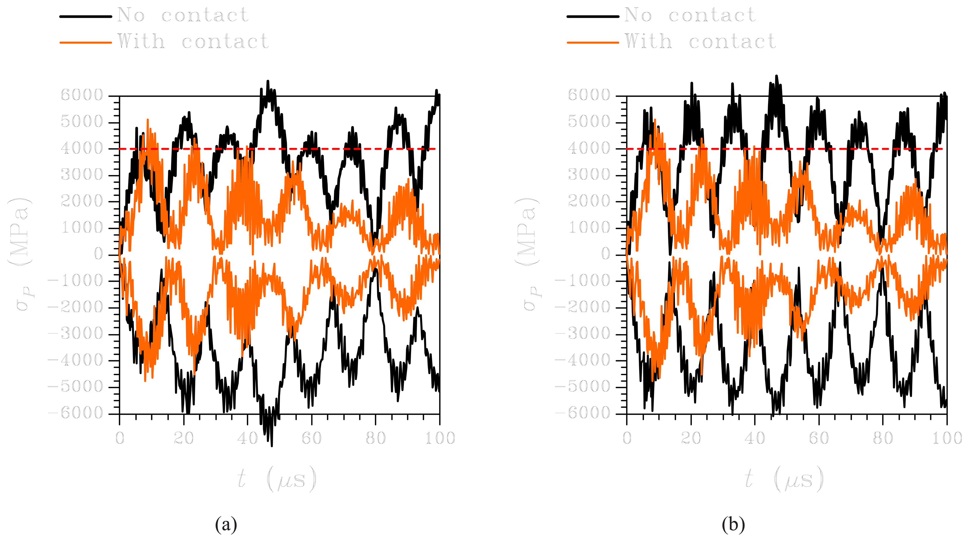
Figures 6 and 7 collect the envelopes of the principal stresses up to tend = 100 μs in the above mentioned joint sections, as caused by bottom and top impacts respectively. When contact between sensor and die is disregarded, it can be noticed that low frequency variations, with period Tlow ≈ 13 μs, are superposed to high frequency ones. These latter ones are linked to higher vibration modes of the springs, but they can be spurious artifacts of the simulations. When interaction between sensor and die is allowed for, vibrations turn out to be damped soon after the seismic mass strikes the die surface.
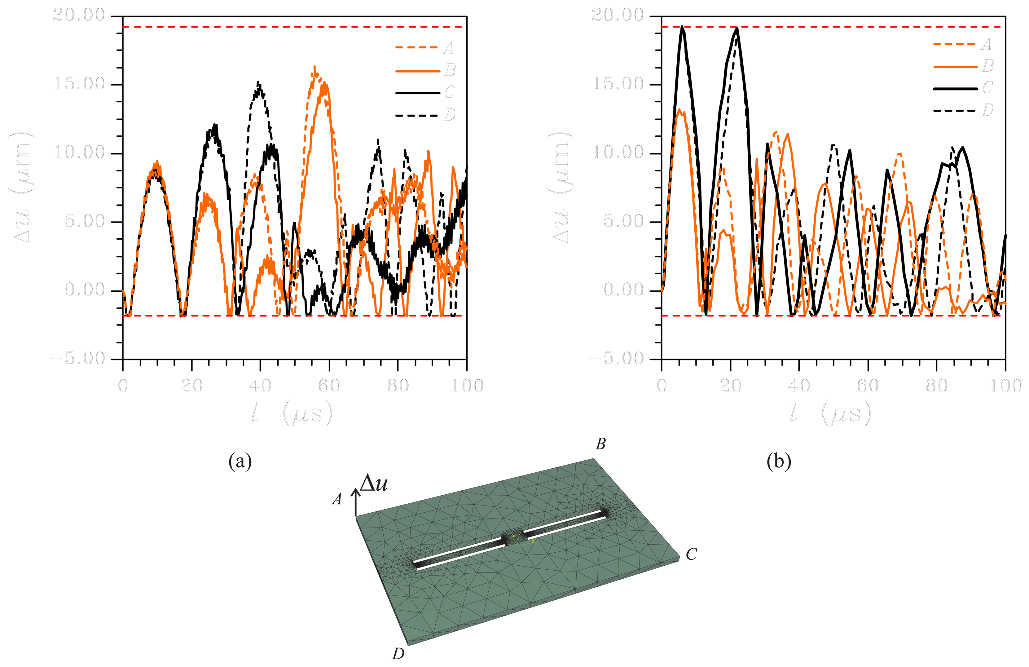
This is clearly evidenced in Figure 8, where the relative displacements between the plate corners and the die/cap surfaces along the direction perpendicular to the plate (sensing direction) are shown. In these plots, when the Δu curves match the horizontal dashed lines it means that the corresponding plate corner (according to the notation of Figure 8) and the top/bottom surfaces of the die cavity come into contact. In the bottom case (Figure 8a) the plate is pushed downwards after the impact by its inertia and the bottom surface of the die cavity is quickly approached: the deflection of the beam and, therefore, the stress field are reduced with respect to the case in which this interaction is disregarded. In the top case (Figure 8b), the sensor falls up-side down and impact against the target surface causes an upward motion of the seismic mass in the reference frame of Figure 2. Since the gap between the accelerometer and the bottom surface of the device cap is far greater that that between the accelerometer itself and the top surface of the die (as revealed by the ordinate of the horizontal lines in Figure 8), the springs suffer in this drop configuration a significant deflection before the interaction sensor-die takes place. This explains why in the top drop the stress field is higher and exceeds the tensile strength of the polysilicon, whereas in the bottom drop this limit is never approached.
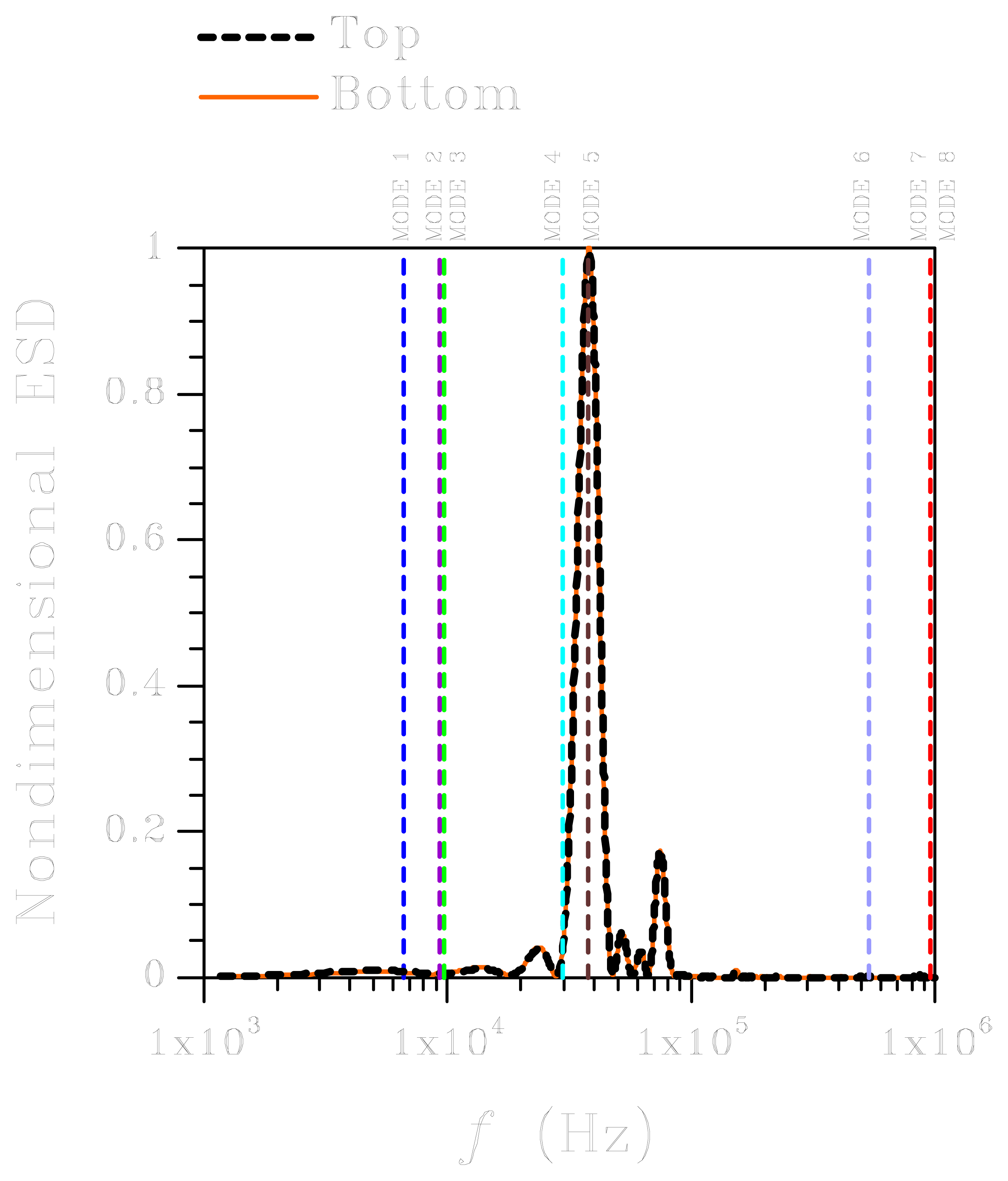
Figure 8 also shows that, even though the sensor falls perfectly horizontal in both the drop configurations, the asymmetric sensor lay-out (set to maximize the sensitivity to the acceleration along axis x3) lead to different relative movement records registered at points A and D, and at points B and C, thereby causing a coupled bending-torsional vibration of the springs. This is also shown by the Fourier transform of the maximum principal stress at the anchor point, see Figure 9: in the two drop configurations, the same peak in the excitation show up at a frequency corresponding to the fifth vibration mode of the sensor. Figure 10 collects the first six vibration modes of the sensor; here, obviously, the interaction between the sensor and the die has been disregarded to avoid nonlinear effects. As anticipated by plots in Figure 8, the fifth mode produces an out-of-plane bending of the springs coupled to longitudinal torsion.
Account taken of the sensor-die interaction, the bottom drop, characterized by higher acceleration peaks at the anchor point in the sensing direction (see Figure 4b), leads to a stress field never exceeding the tensile strength of the polysilicon. Overturning the conclusion at the macro-scale, the top drop, characterized by lower acceleration peaks at the sensor anchor, leads to stress envelopes actually exceeding the material tensile strength around 10 μs after the impact. Hence, while the acceleration records lead to the conclusion the the bottom drop is more critical, micro-scale analyses reveal that only the top drop gives rise in this case to a stress field that could brake the spring-anchor joint section. As already pointed out in what precedes, if the actual failure mechanism in this section needs to be modeled, one has to account for a representative crystal structure of the MEMS in the surrounding region.
To better understand the effects of the impact on the sensor dynamics, animations in Figures 11 and 12 (relevant to the bottom drop), and in Figures 13 and 14 (relevant to the top drop) show isometric and lateral views of the vibrating sensor in the interval 0 < t < 25 μs (displacements are here amplified five times). As for the top case, the accelerometer is shown upside-down, in its actual drop configuration. It can be seen that in both cases a stress concentration, localized around the end sections of the springs, is triggered by the MEMS layout.
5. Conclusions
In this paper we have proposed a multi-scale numerical approach to compute the stress state induced in polysilicon MEMS sensors by accidental drops, and to detect eventual failure locations. Macro-scale simulations (at die length-scale) furnish the displacement histories at sensor anchor points, to be used as input loading condition in meso-scale analyses (at sensor length-scale).
It has been shown that, depending on how the sensor interacts with die/cap, the acceleration peak is not an objective indicator as far as the safety of the device is concerned. In fact, the suspension springs of the sensor are subject to a coupled flexural/torsional deformation mode and can locally fail at their end sections if stoppers and die/cap surfaces do not constrain enough the displacement of the seismic mass.
While the proposed approach furnishes accurate outcomes as for the identification of critical drop configurations, micro-scale analyses (at polysilicon length-scale) should be adopted to get insights into the possible failure mechanisms typically caused by inter- as well as trans-granular crack growth.
Acknowledgments
The support of EU NoE Design for Micro & Nano Manufacture (Patent DfMM), contract no. 509255 is gratefully acknowledged. A.G. wishes to thank Cariplo Foundation for the financial support of the project Innovative models for the study of the behaviour of solids and fluids in micro/nano electromechanical systems. S.M. gratefully acknowledges the financial support of Italian MIUR through PRIN-Cofin2005 programme Interfaces in innovative micro and nano structured materials and devices.
References
- Suhir, E. Is the maximum acceleration an adequate criterion of the dynamic strength of a structural element in an electronic product? IEEE Transactions on Components, Packaging and Manifacturing Technology 1997, 20, 513–517. [Google Scholar]
- Li, G.; Shemansky, F. Drop test and analysis on micro machined structures. Sensors and Actuators A 2000, 85, 280–286. [Google Scholar]
- Hauck, T.; Li, G.; McNeill, A.; Knoll, H.; Ebert, M.; Bagdahn, J. Drop simulation and stress analysis of MEMS devices. Ernst, L. J., Zhang, G. Q., Rodgers, P., Meuwissen, M., Marco, S., de Saint Leger, O., Eds.; In Proc. Eurosime06; pp. 203–207. Como (Italy), April 2006. [Google Scholar]
- Cho, S.; Jonnalagadda, K.; Chasiotis, I. Mode I and mixed mode fracture of polysilicon for MEMS. Fatigue and Fracture of Engineering Materials and Structures 2007, 30, 21–31. [Google Scholar]
- Boroch, R.; Wiaranowski, J.; Mueller-Fiedler, R.; Ebert, M.; Bagdahn, J. Characterization of strength properties of thin polycrystalline silicon films for MEMS applications. Fatigue and Fracture of Engineering Materials and Structures 2007, 30, 2–12. [Google Scholar]
- Espinosa, H.; Zavattieri, P. A grain level model for the study of failure initiation and evolution in polycrystalline brittle materials. Part I: theory and numerical implementation. Mechanics of Materials 2003, 35, 333–364. [Google Scholar]
- Corigliano, A.; Cacchione, F.; Frangi, A.; Zerbini, S. Simulation of impact rupture in polysilicon MEMS. Ernst, L. J., Zhang, G. Q., Rodgers, P., Meuwissen, M., Marco, S., de Saint Leger, O., Eds.; In Proc. Eurosime06; pp. 197–202. Como (Italy), April 2006. [Google Scholar]
- Corigliano, A.; Cacchione, F.; Frangi, A.; Zerbini, S. Micro-scale simulation of impact rupture in polysilicon MEMS. Gdoutos, E. E., Ed.; In Proc. ECF16; Alexandropoulos (Greece), July 2006.
- Falcon, E.; Laroche, C.; Fauve, S.; Coste, C. Collision of a 1-D column of beads with a wall. The European Physical Journal B 1998, 5, 111–131. [Google Scholar]
- Srikar, V.; Senturia, S. The reliability of Microelectromechanical systems (MEMS) in shock environments. Journal of Microelectromechanical Systems 2002, 11, 206–214. [Google Scholar]
- Zavattieri, P.; Espinosa, H. Grain level analysis of crack initiation and propagation in brittle materials. Acta Materialia 2001, 49, 4291–4311. [Google Scholar]
- Cho, S.; Chasiotis, I. Elastic properties and representative volume element of polycrystalline silicon for MEMS. Experimental Mechanics 2007, 47, 37–49. [Google Scholar]
- Zienkiewicz, O. C.; Taylor, R. L. The finite element method: the basisvolume 1, Butterworth-Heinemann Oxford, 5th edition; 2000. [Google Scholar]
- Brantley, W. A. Calculated elastic constants for stress problems associated with semiconductor devices. Journal of Applied Physics 1973, 44, 534–535. [Google Scholar]
- Mullen, R. L.; Ballarini, R.; Yin, Y.; Heuer, H. Monte Carlo simulation of effective elastic constants of polycristalline thin films. Acta Materialia 1997, 45, 2247–2255. [Google Scholar]
- Nye, J. F. Physical properties of crystals.; Clarendon: Oxford, 1985. [Google Scholar]
- Chasiotis, I.; Knauss, W. G. The mechanical strength of polysilicon films. Part 2: size effect associated with elliptical and circular perforations. Journal of the Mechanics and Physics of Solids 2003, 51, 1551–1572. [Google Scholar]
- Weibull, W. A statistical distribution of wide applicability. Journal of Applied Mechanics 1951, 18, 293–297. [Google Scholar]
- Corigliano, A.; Cacchione, F.; De Masi, B.; Riva, C. On-chip electrostatically actuated bending tests for the mechanical characterization of polysilicon at the micro scale. Meccanica 2005, 40, 485–503. [Google Scholar]
Figure 1.
Sketch of the polysilicon film, showing a columnar grain assembly with growth direction aligned with axis x3. The reference frame for each single crystal represents the relevant orientation of the local privileged directions (or axes of elastic symmetry).
Figure 1.
Sketch of the polysilicon film, showing a columnar grain assembly with growth direction aligned with axis x3. The reference frame for each single crystal represents the relevant orientation of the local privileged directions (or axes of elastic symmetry).

Figure 2.
Overview of the die mesh.

Figure 3.
Snapshots of the bouncing die, taken every 20 μs after the impact event: (left) bottom drop; (right) top drop.
Figure 3.
Snapshots of the bouncing die, taken every 20 μs after the impact event: (left) bottom drop; (right) top drop.

Figure 4.
Comparison between top and bottom acceleration histories (a) in the full analysis range 0 < t < 100 μs and (b) in the short-time interval 0 < t < 2 μs after the impact.
Figure 4.
Comparison between top and bottom acceleration histories (a) in the full analysis range 0 < t < 100 μs and (b) in the short-time interval 0 < t < 2 μs after the impact.

Figure 5.
Overview of the sensor mesh and detail of the spring-anchor point.

Figure 6.
Bottom drop: stress envelopes (a) at the spring-anchor joint sections and (b) at the spring-plate joint sections.
Figure 6.
Bottom drop: stress envelopes (a) at the spring-anchor joint sections and (b) at the spring-plate joint sections.

Figure 7.
Top drop: stress envelopes (a) at the spring-anchor joint sections and (b) at the spring-plate joint sections.
Figure 7.
Top drop: stress envelopes (a) at the spring-anchor joint sections and (b) at the spring-plate joint sections.

Figure 8.
Relative out-of-plane displacements at plate corners: (a) bottom drop; (b) top drop.

Figure 9.
Stress-related nondimensional energy spectral density at the anchor point.

Figure 10.
First vibration modes of the sensor (displacements are amplified in the plots to help understanding the deformation type).
Figure 10.
First vibration modes of the sensor (displacements are amplified in the plots to help understanding the deformation type).

Figure 11.
Bottom drop: lateral view of the vibrating sensor in the interval 0 < t < 25 μs.
Figure 12.
Bottom drop: isometric view of the vibrating sensor in the interval 0 < t < 25 μs.
Figure 13.
Top drop: lateral view of the vibrating sensor in the interval 0 < t < 25 μs.
Figure 14.
Top drop: isometric view of the vibrating sensor in the interval 0 < t < 25 μs.
© 2007 by MDPI ( http://www.mdpi.org). Reproduction is permitted for noncommercial purposes.
Share and Cite
MDPI and ACS Style
Mariani, S.; Ghisi, A.; Corigliano, A.; Zerbini, S. Multi-scale Analysis of MEMS Sensors Subject to Drop Impacts. Sensors 2007, 7, 1817-1833. https://doi.org/10.3390/s7081817
AMA Style
Mariani S, Ghisi A, Corigliano A, Zerbini S. Multi-scale Analysis of MEMS Sensors Subject to Drop Impacts. Sensors. 2007; 7(9):1817-1833. https://doi.org/10.3390/s7081817
Chicago/Turabian StyleMariani, Stefano, Aldo Ghisi, Alberto Corigliano, and Sarah Zerbini. 2007. "Multi-scale Analysis of MEMS Sensors Subject to Drop Impacts" Sensors 7, no. 9: 1817-1833. https://doi.org/10.3390/s7081817