An Optical Tomography System Using a Digital Signal Processor

1
Control & Instrumentation Engineering Department, Faculty of Electrical Engineering, Universiti Teknologi Malaysia, 81310 Skudai, Johor Bahru, Malaysia
2
School of Mechatronic Engineering, Universiti Malaysia Perlis, 02600 Arau, Perlis, Malaysia
*
Author to whom correspondence should be addressed.
Sensors 2008, 8(4), 2082-2103; https://doi.org/10.3390/s8042082
Submission received: 29 January 2008
/
Accepted: 7 March 2008
/
Published: 27 March 2008
Abstract
:The use of a personal computer together with a Data Acquisition System (DAQ) as the processing tool in optical tomography systems has been the norm ever since the beginning of process tomography. However, advancements in silicon fabrication technology allow nowadays the fabrication of powerful Digital Signal Processors (DSP) at a reasonable cost. This allows this technology to be used in an optical tomography system since data acquisition and processing can be performed within the DSP. Thus, the dependency on a personal computer and a DAQ to sample and process the external signals can be reduced or even eliminated. The DSP system was customized to control the data acquisition process of 16×16 optical sensor array, arranged in parallel beam projection. The data collected was used to reconstruct the cross sectional image of the pipeline conveyor. For image display purposes, the reconstructed image was sent to a personal computer via serial communication. This allows the use of a laptop to display the tomogram image besides performing any other offline analysis.
1. Introduction
Optical tomography involves the use of non-invasive optical sensors to obtain vital information in order to produce images of the dynamic internal characteristics of process system [4]. The use of optical sensors has the advantages of being conceptually straightforward and relatively inexpensive [7]. Its working principle involves projecting a beam of light through a medium from one boundary point and detecting the level of light received at another boundary point [9]. A typical optical tomography system usually uses a Data Acquisition System (DAQ) to perform data acquisition tasks and a host computer to carry out image reconstruction. However, only some of the functions provided by the DAQ were implemented. This is a waste of resources considering the high cost of a DAQ system. This paper discusses the implementation of DSP as the core processor in a parallel beam projection optical tomography system.
On the other hand, nowadays powerful Digital Signal Processors (DSP) running at Millions Instructions Per Second (MIPS) are available at very reasonable cost. A DSP, which is usually equipped with single cycle multiplication, is well suited for number crunching applications and optimized for digital signal processing algorithms. The tasks that were carried out by the DAQ and host computer such as data acquisition and image reconstruction can now be carried out by the DSP alone. However, the host computer is still needed for display purposes. Alternatively, a Liquid Crystal Display (LCD) could be utilized to display the results.
The full automation of solid-handling plant has frequently not been possible because of the lack of a basic flow meter [3]. The previously used technique to measure solid flow often involved removing the material for weighing which was complicated, expensive and did not allow continuous feedback for automatic control [3]. Many non intrusive techniques attempted to measure solids mass flow in pneumatic conveyor were elaborated Beck et al. [1].
Later, Xie et al. [13] made an effort to measure mass flow of solids in pneumatic conveyors by combining electrodynamics and capacitance transducers. Rahim et al. [10] investigated applications of fibre optics into optical tomography for flow concentration measurement. Chan [2] followed up and investigated mass flow rate measurement using optical tomography by relating the flow's concentration profile measurement with its mass flow rate. This method first performs calibration by recording the flow's concentration percentage plotted against mass flow rate measured using weight scale and stop watch. Based on their findings, the two variables had linear relation in light flow condition. However, this technique requires re-calibration each time a new flow material is used.
Cross correlation technique was proposed by Beck et al. [1] for flow velocity measurement. This function was successfully applied by Ibrahim and Green [5] for offline bubble flow velocity measurement using optical tomography. In 2003, Pang [7] implemented real time system for solid-gas flow concentration, flow velocity and mass flow rate measurement using optical tomography and data distribution system. The cross correlation techniques being used by these researches were based on time domain cross correlation function, which was very time consuming.
Pang [7] implemented four projections arrays (2 orthogonal and 2 rectilinear) in optical tomography system. The extra two layers (the Rectilinear layers) were used to filter the ambiguous image and smearing effects. However, analogue acquisition was used to acquire all the measurements. The obtained data from masking layer were used for comparison to predetermined threshold values. Using this method, valuable time was utilized for analogue to digital conversions. Furthermore, the number of sensors on the rectilinear was quite large. Although the research successfully implemented real time optical tomography system, it required four powerful personal computers and a network hub in order to implement data distribution system. The resulting system was bulky and not portable.
2. Hardware Construction
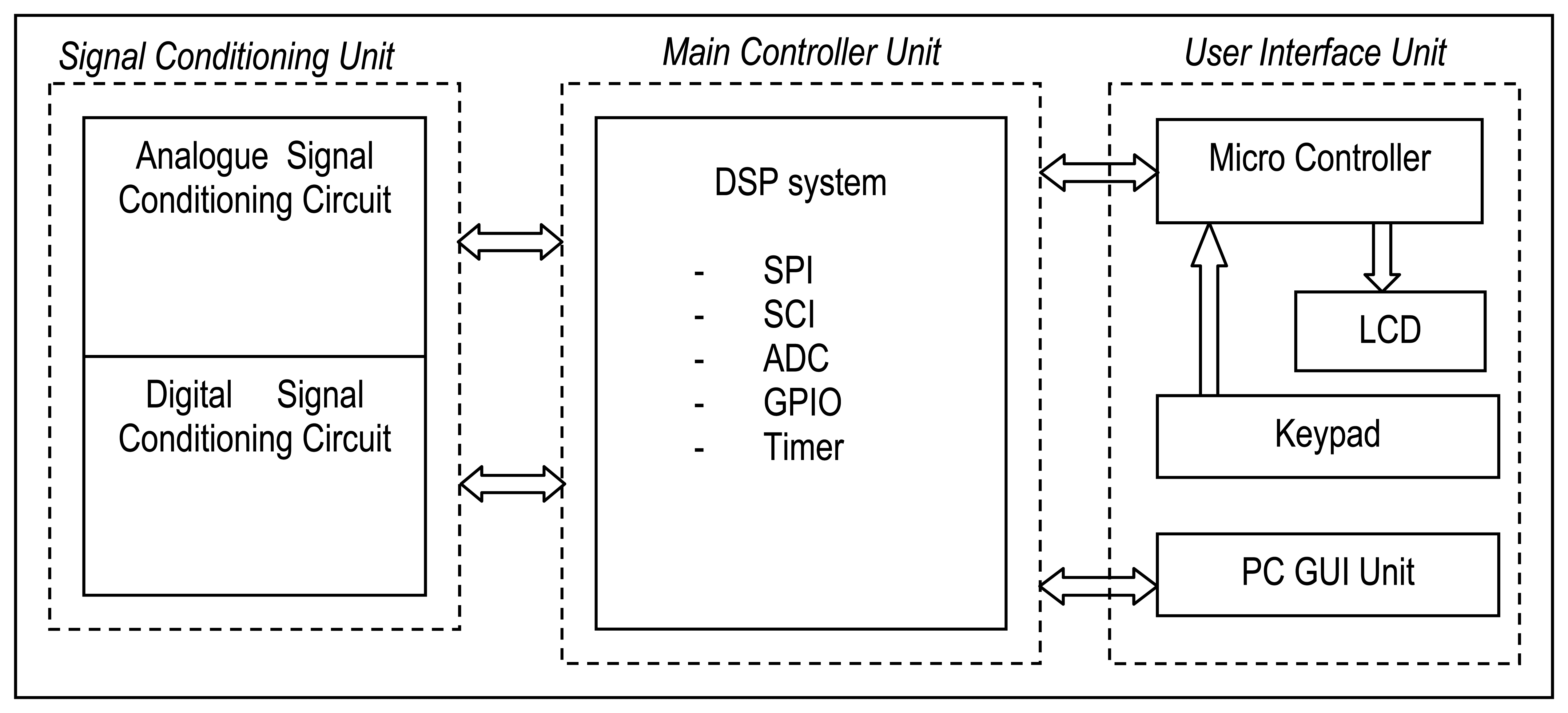
The topology is illustrated in Figure 1. The first module, which is the Signal Conditioning Unit, is responsible for the conditioning of incoming signals from the optical sensors. For Analogue Signal Conditioning, the incoming signals are from 64 optical sensors of the orthogonal layers. These signals are multiplexed into 16 ADC channels on the DSP system. On the other hand, 92 single bit binary streams from the Digital Signal Conditioning are sent to the embedded system using Serial Peripheral Interface (SPI). There are also signals from the DSP system to control the sampling process of these two modules.
The Main Controller Unit, as its name implies, acts as a main controller in processing the measurement data and producing required results. It is mainly used to perform the thousands of calculations required for image reconstruction algorithms, velocity profile construction and mass flow rate measurements. It also coordinates the communication between Signal Conditioning Unit and User Interface Unit.
2.1. Sensor Configuration
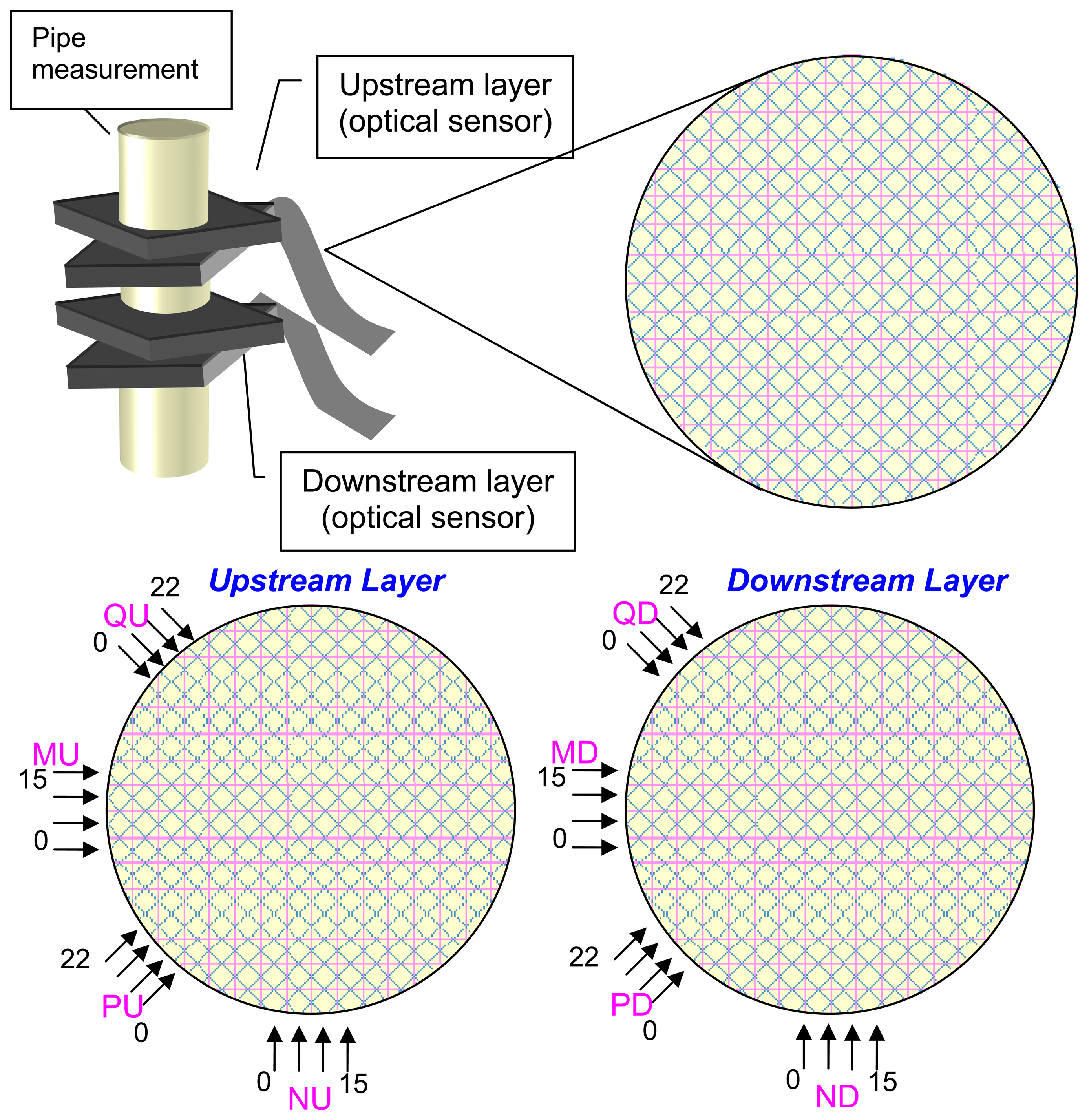
In this research, a fabricated optical sensor unit with sensors arranged in parallel beam projection has been implemented [8]. There are two layers of sensors being used, namely Upstream Layer and Downstream Layer to support the analysis of algorithm-based velocity profile measurement. At each layer, there are four arrays of sensors arranged in parallel beam projections. Two arrays of sensors, namely Orthogonal Sensors are arranged in such a way that their projected light beams are orthogonal (90°) to each other while another 2 arrays of sensors namely, Rectilinear Sensors are arranged so that their projected light beams are 45° to the orthogonal projections. This configuration is illustrated in Figure 2.
There are 16 sensors at each orthogonal projection (MU0–MU15, NU0–NU15, MD0–MD15, ND0–ND15) where altogether is a total of 64 sensors. The suffix U and D appended were to represent the Upstream and Downstream layer. Another four arrays of 23 sensors (PU0–PU22, QU0–QU22, PD0–PD22, QD0–QD22) are arranged to provide rectilinear projections. This adds up 92 sensors for the rectilinear projections for Upstream and Downstream layers. In total, there are 156 sensors readings to be acquired at every single scan.
3. Signal Conditioning Unit
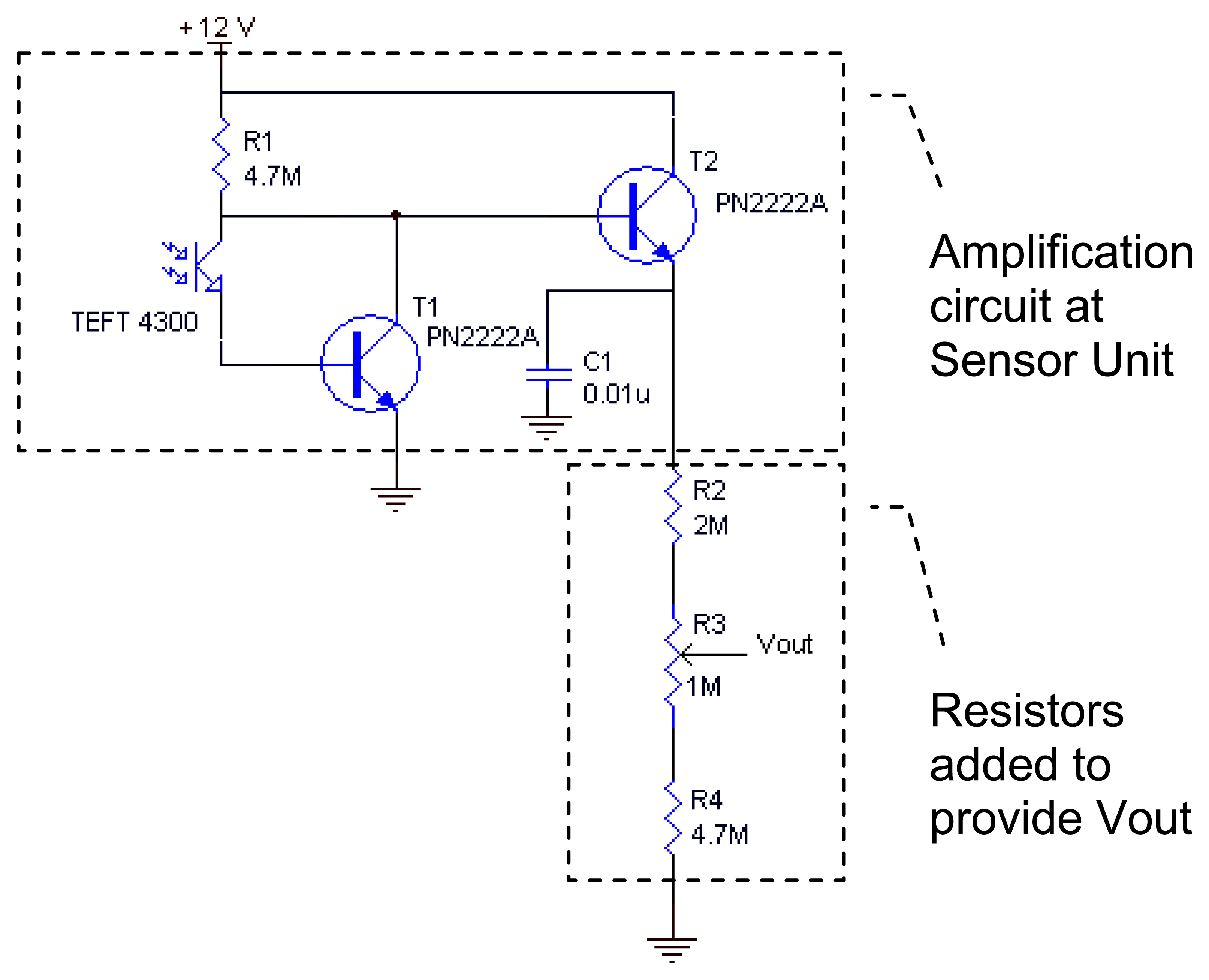
The Sensor Unit already includes LED driver circuits and amplifier circuits to convert the received light to electrical signals. Each sensor from the Sensor Unit outputs a current which is inversly proportional to the light intensity it measures. In other words, higher current is output when there is little light (object presence blocks the light beam) and lower current is output when there is more light (no object blocking the light beam). This way, software overhead is reduced during image reconstruction as the presence of object is proportional with the voltage measured. In work by Chan [2], optical attenuation model was used, where object presence resulted in voltage loss. The processing software then subtracted the loss from the expected full voltage to obtain the correct readings. This step was not required in this research.
All the signal amplifiers on the Sensor Unit are identical. Only resistors must be added to the outputs of the Sensor Unit to have a voltage drop for measurement. The circuit for a single sensor is shown in Figure 3. In this circuit, R2, R3 and R4 are used as simple current to voltage converter. R3 is a variable resistor, specifically used to adjust the scale of Vout. The value of 1MΩ is about 12.5% of the total drop voltage. This allows adjustment to calibrate optical sensors.
In designing the signal conditioning circuits, there are two considerations that need to be observed. The first consideration is the data acquisition rate. In total, there are 156 sensors readings to be acquired at every single scan. This obviously causes the measurement to take very long time, especially using a single digitizer with low conversion rate. Using a low conversion rate digitizer, an array of sample and hold circuit is required to acquire and hold the readings of a single scan [7]. This is because the conversions occur sequentially and by the time the digitizer converts the next sensor, the current signal is not from the same time as captured by the previous sensors. This may result in tilted or distorted image. Since there are 156 sensors on the sensor unit, using sample and hold circuits for each sensor will also take up a lot of board space.
Another approach is to speed up measurement time by using dedicated low conversion rate digitizer per sensor or per group of sensors. The digitizers can be triggered to convert many signals simultaneously so that the need of sample and hold circuits can be eliminated. However, this approach is expensive and still occupies a lot of board space.
As a solution, a high conversion rate ADC was implemented in this research to overcome the said issues. The use of a single high conversion rate ADC required analogue multiplexers to multiplex respective signals for conversion. In this research, the ADC being used was built-in inside the DSP chip. Internally, it was multiplexed to receive analogue signals from 16 external channels. Since there are more than 16 signals for conversion, additional analogue multiplexers still need to be designed.
As for the second consideration, a faster method compared to ADC for sampling the sensors on rectilinear projections is desired. This is because these sensors only provide masking of ambiguous image in Hybrid Reconstruction algorithm. Previously, these signals were converted using ADC and compared to a threshold value set in software [7]. If the measured signal value was above the threshold value, a TRUE value was obtained and vice versa. Then, the signal value was discarded. Therefore, a single bit binary representation is sufficient and this can be implemented using hardware voltage comparator which can perform this same task at a higher rate. This approach reduces the number of signals for ADC conversion from 156 signals to only 64 signals.
3.1. Analogue Signal Conditioning Circuit
Basically, the Sensor Unit has provided the amplifications to convert the light intensity to current. Resistors were added to the output of the amplifier circuits to generate voltage drop for measurement. The fabricated circuits on the sensor unit were based on optical path width model [7] where the current outputs correlate linearly with the width of the object that obstructs the light beam.
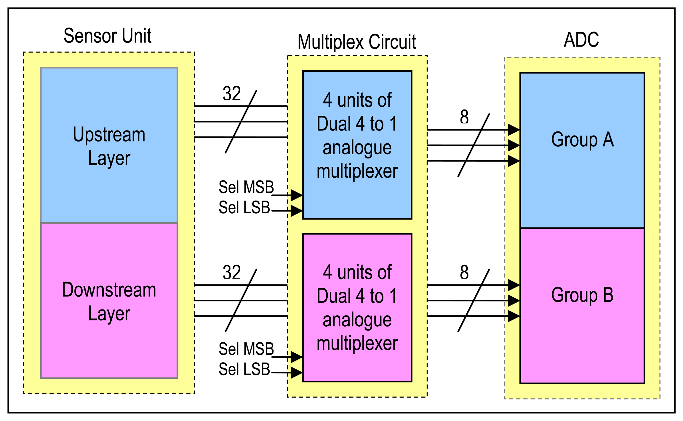
As mentioned previously, there are 16 sensors per projection and there are two orthogonal projections per layer. Therefore, there are 32 signals for Upstream Layer and 32 signals for Downstream Layer, totalling up to 64 signals for measurement. In this research, a built in ADC in a DSP of the Main Controller Unit was utilized to perform the signal acquisitions.
The ADC is multiplexed into two groups, namely Group A and Group B. Each group consists of eight channels, thus expanding the total channel inputs of the ADC to be 16 channels. Due to the fact that there are 64 signals to convert, the signals need to be multiplexed. Four dual 4 to 1 analogue multiplexers (4052) were used per layer to multiplex these signals. Using this configuration, all 64 channels measurements can be accomplished in four acquisitions. The dual 4 to 1 analogue multiplexer was also chosen instead of the 8 to 1 analogue multiplexer since there were 16 ADC channels that were available. The data acquisition process can also be controlled easily since only two input bits (Sel MSB and Sel LSB) need to be controlled by using GPIO port. The overall configuration is shown in Figure 4.
3.2. Digital Signal Conditioning Circuit
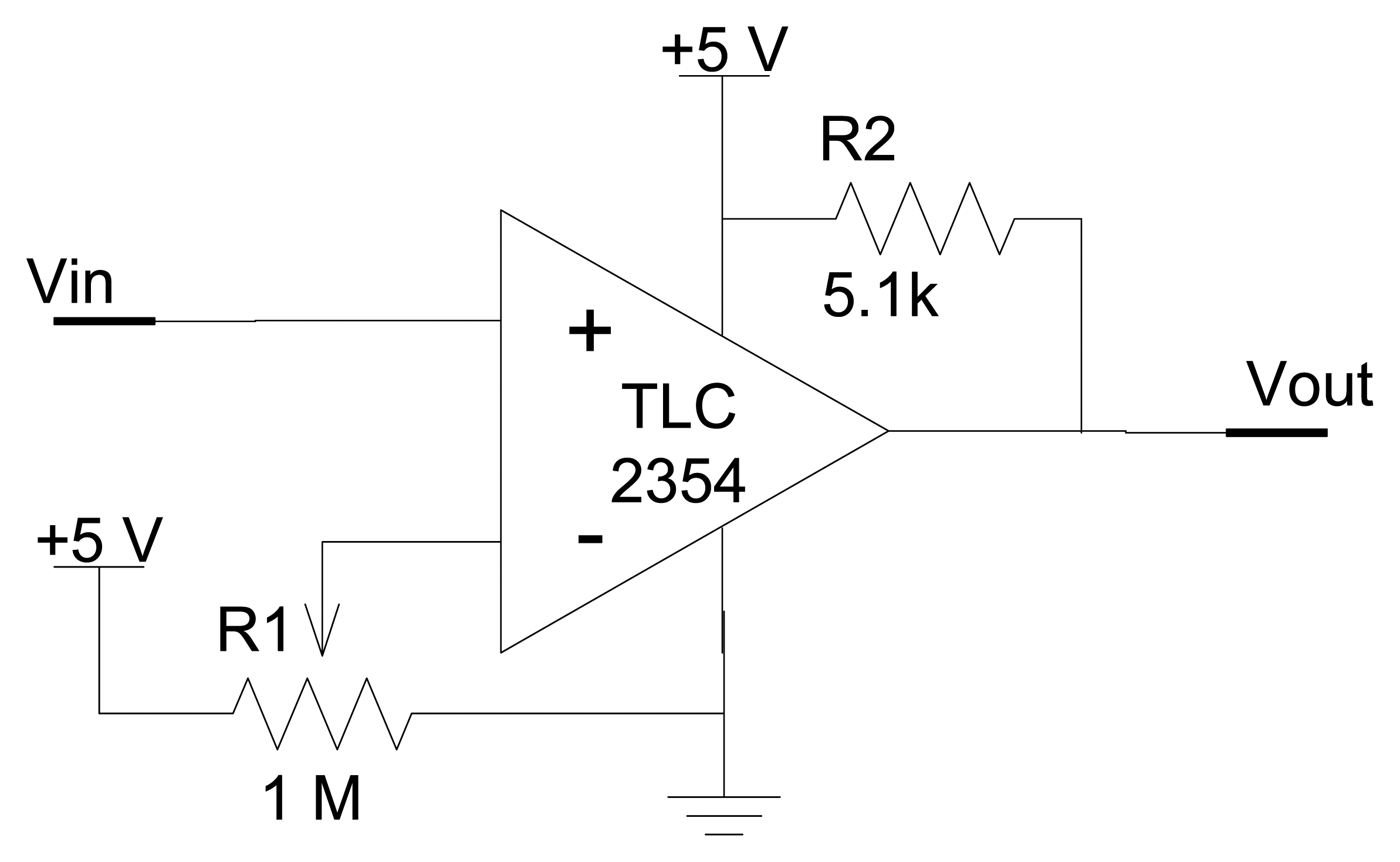
As discussed in Section 3, improvement on the sampling method of the sensors for rectilinear projections was implemented using hardware voltage comparator. As the rectilinear projections were really used as a masking layer (to filter ambiguous image obtained from orthogonal projections), a single bit representation is sufficient (Either TRUE or FALSE). This is a trade off of more information (as in analogue values) with simpler and quicker processing. Each voltage comparator is implemented using TLC 2354 referenced to a voltage divider using variable resistor. These variable resistors were calibrated to a threshold value of about 25% of the steady state sensor output voltage (4V). This made sure that the representation was valid and not caused by false trigger such as noise and spikes. The following Equation 1 represents the value of the binary bit for different sensor voltage levels.
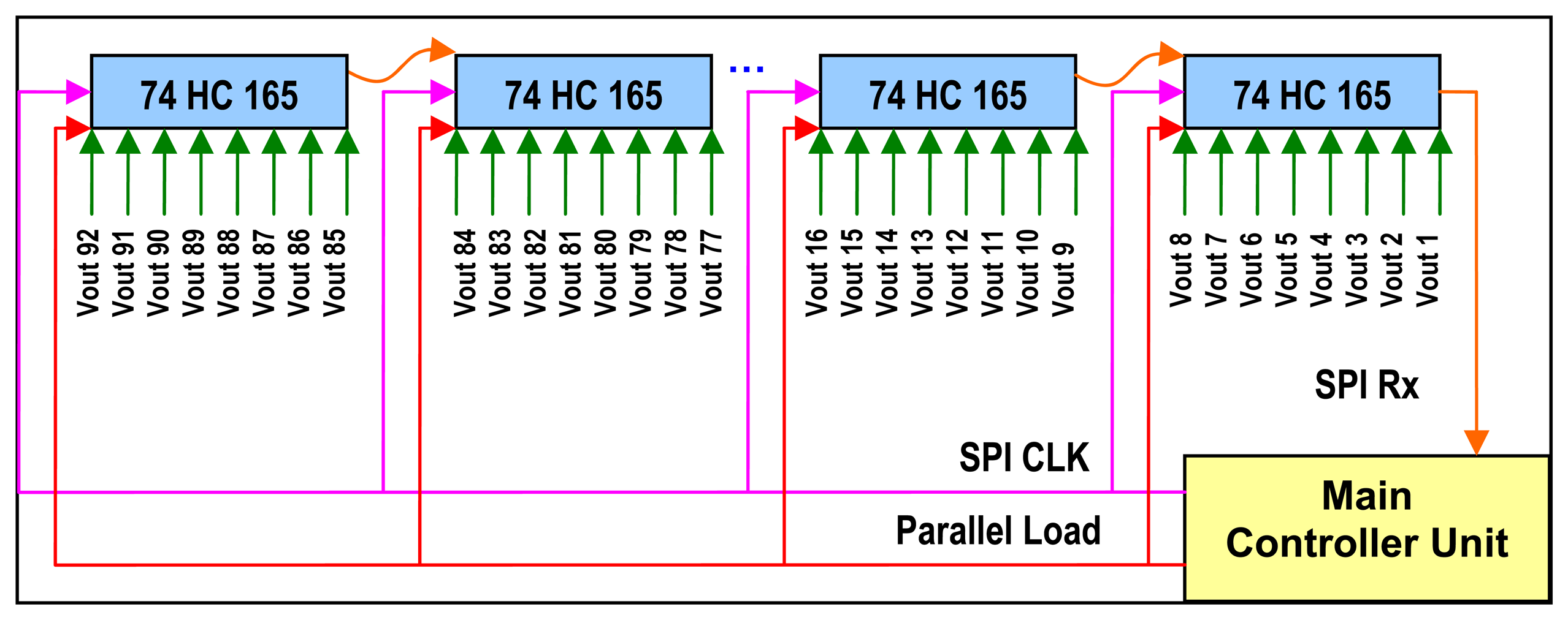
The circuit for each voltage comparator is shown in Figure 5. After the voltage comparisons were carried out, the binary bits need to be sent to the embedded system. This was conveniently achieved by converting them to serial bit stream and then reading the data using Serial Peripheral Interface (SPI). Each sensor output from the rectilinear projections was fed to a voltage comparator input (Vin).
The resulting outputs (Vout) from the comparators were then connected to the data inputs of parallel to serial converter chips (74HC165) arranged in cascade. The embedded system only needed to load the parallel data bits by sending a pulse to the Parallel Load pin and generate clock signal to shift in the serial data. From the embedded system side of view, the Digital Signal Conditioning Circuit is merely a slave device with serial interface. This approach is less troublesome compared with using bus topology where buffers and more digital input and output lines are needed [12]. Besides that, the chip is able to support high speed data transfer. The overall topology of the digital signal conditioning circuit is shown in Figure 6.
4. Main Controller Unit
The main controller unit is the brain of the whole system. The processing involved includes data acquisition, image reconstruction from measured sensors signals, flow analysis in terms of flow velocity and mass flow rate measurement and communication between modules. All these processes require intensive calculations and thus, the performance of this controller is very essential in affecting the overall system performance. Pang [8] developed an optical tomography that could perform image reconstruction in real time by using data distribution system where 3 sets of high performance PC (2.4 GHz, 512 MB RAM) were used. This research attempted to achieve comparable result using only single embedded system as its main controller unit.
Among the criteria that need to be fulfilled by the embedded system are high execution speed, low cost, support for standard communication protocols and memory expansion capability [8]. Micro processor based systems can offer high flexibility but requires more complicated design and other peripheral interfaces to support required functionalities. On the other hand, micro controller based systems offers many built in and ready to use standard peripherals but are usually not very flexible. Finally, a Digital Signal Processor based system provides relatively greater performance but lacks in terms of interfacing to the outside world.
A relatively new technology was introduced to the market lately and was known as the Hybrid Digital Signal Processor. The hybrid term was actually a combination of the micro controller and Digital Signal Processor technologies. As such, this architecture is actually a solution that benefits the best of both worlds. As this research requires both the peripherals offered by micro controller and high speed processing offered by Digital Signal Processor, the Hybrid Digital Signal Processor makes a very suitable choice as the platform for implementation in this research.
A comparison was carried out on some of the Digital Signal Processors offered by Texas Instruments Inc. [11] and the results are shown in Table 1. It can be concluded that the most suitable processor for this research is the one from the TMS320F28xx family. A device from this family, TMS320 F2812 fulfils almost all of the requirements needed. The unavailability of the Floating Point Unit is considered as a trade off for its low cost and can be justified by many of the supporting peripherals that come together in the chip.
5. Digital Signal Processor Architecture
The chosen DSP (TMS320 F2812) as the main controller in the embedded system is a well equipped architecture with many essential peripherals built in and ready to be used. These peripherals include the internal high speed Analogue to Digital Converter (ADC), Serial Peripheral Interface (SPI), Serial Communication Interface (SCI) and 16 bit Timer.
5.1. User IO Unit
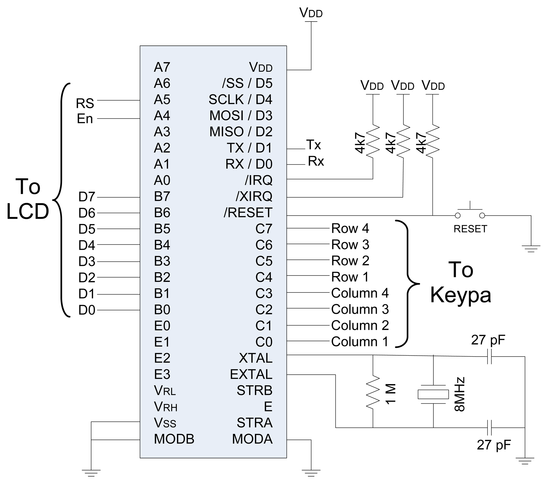
As mentioned previously, this unit allowed user to view Mass Flow Rate result and change certain settings of the Main Controller Unit. This unit consists of a microcontroller, LCD module and a 4×4 matrix keypad. By implementing this module, the control of LCD and keypad processing became transparent to the Main Controller Unit. Hence, the Main Controller Unit was able to communicate with this module using only the serial communication interface.
5.2 The Microcontroller Architecture
The User IO Unit was developed using M68HC11 microcontroller from Motorola Inc. This microcontroller which is commonly known as HC11 contains many built in peripherals such as SCI, SPI, RAM, EEPROM, ADC, GPIO and Timing modules. It is typically driven by an 8 MHz crystal oscillator, which provides a main clock speed of 2 MHz (the main clock rate divided by four). For LCD display and keypad handling purposes, this speed is sufficient. Shown in Figure 7 is the circuit diagram for the User IO Unit. Basically, the circuit is a minimum system that uses its GPIO pins to drive the necessary signals to the LCD module and decode the keypad.
5.3. Liquid Crystal Display (LCD)
The Liquid Crystal Display is a standard 2 lines, 16 characters alphanumeric LCD module. The alphanumeric display is actually driven by a LCD driver built-in in the module. The LCD driver contains a table of standard alphanumeric characters stored in its volatile memory. Commands and data are sent to this driver by driving the necessary pins to certain patterns. Figure 8 shows the connections of the LCD module to the embedded system.
In order to display data to the LCD module, standard protocol and commands set were used. These commands are usually standard among most LCD modules. Basically, the microcontroller needs to handle the control signals according to certain timing requirements and outputs the command or data to the data bus accordingly.
5.4. Keypad
The main usage of the keypad is as the input interface for the user when the PC GUI unit is not being used. Settings such as solid density and status of PC GUI unit (online or offline) are inputs that can be entered through this interface. The keypad used in this research is a standard 4×4 matrix keypad. This interface acts as an input to user to change settings if required. The microcontroller is responsible to decode the key pressed by the user and send it to the Main Controller Unit.
6. Firmware Development
6.1. System Flowchart
The overall operation performed by the DSP is described in Figure 9. Basically, the system was initialized at program start to set the configurations of ADC, SPI and SCI such as ADC channel sampling sequence, SCI and SPI bit length, parity and baud rate. After being initialized, data acquisition began by sending a pulse to Parallel Load pin on parallel to serial converters. This action latched the binary outputs from the comparator into the converter. Then, acquisition from rectilinear projection sensors was carried out by reading data from SPI. The use of SPI caused the binary values to be packed in six words, so they were unpacked into variables after the acquisition.
As for the orthogonal projections, the Select pins on the analogue multiplexers were set from 0 to 3 to multiplex 64 channels into the ADC. The Select pin setting and the respective channels being multiplexed are shown in Table 2 below.
Two image reconstruction algorithms were implemented in this study. The first algorithm was the commonly known Linear Back Projection algorithm while the second algorithm was the Hybrid algorithm [5]. The image reconstructed was stored in internal Random Access Memory (RAM) of the DSP. Finally, the DSP sent the image to the host computer upon request via SCI. At the host computer, a Graphical User Interface (GUI) was developed using Ms. Visual C++ to facilitate this feature.
6.2. Hybrid Image Reconstruction Algorithm
In order to visualize the flow concentration using tomography technique, image reconstruction algorithm was applied to the measurement data. The Hybrid reconstruction algorithm which originated from the Linear Back Projection algorithm was implemented with some improvements. Basically, the back projection algorithm can be illustrated as in Figure 10.
Figure 10 (a) shows the actual object and light projection while Figure 10 (b) shows the image reconstructed using Linear Back Projection algorithm. Considering only a single object, this algorithm worked fine (only single pixel detected, shown by dark green) with some smearing, shown by light green. The values shown are the summation of the sensor voltage where sensor voltage is assumed to be 5V if blocked by object. Therefore, the detected pixel shows value of 10V. However, when there is more than one object, the Linear Back Projection algorithm results in ambiguous image as in Figure 11. Notice that there are four pixels ‘detected’ while there are only two actual objects. This is actually a result of summation of the smearing effects.
Based on work by Ibrahim et al. [4] ambiguous image can be eliminated by using at least four projections. He added two rectilinear projections to eliminate ambiguous image and named the image reconstruction algorithm as Hybrid Reconstruction algorithm. Pang [7] further improved this algorithm by doubling the resolution obtained from the previous research which used 8×8 sensor pairs in the orthogonal layer and 11×11 sensor pairs in the rectilinear layer [4] to 16×16 sensor pairs in the orthogonal layer and 23×23 sensor pairs in the rectilinear layer.
Basically, the additional number of sensors used in rectilinear layer was to project the masking layer's beam of light at the centre of each pixel, whereby object's presence at any pixel could be detected with only four sensor readings (two from orthogonal and two from rectilinear). In this research, the same hybrid image reconstruction algorithm was improved by further dividing each pixel into eight small triangles. This is shown in Figure 12.
Although the pixel was divided into 8 small triangles, four triangles in the centre were grouped as one since there wasn't any way to determine the smaller triangles' concentration independently based on the sensor readings. Thus, there were 5 parts, namely A, B, C, D and E. Object that is present at any of these 5 parts could be determined by back projecting the respective sensor readings. By dividing the pixel into 5 smaller parts, each of the small parts can be set as valid or invalid during concentration calculation. This differs from previous work by Pang where the whole pixel was set to a concentration value (using orthogonal layer values) upon confirming that an object exists at that pixel (using only 2 rectilinear layer values).
Using this approach, detection of arc edges of flow object can be presented more accurately. As a fair comparison, let's consider a pixel which is located at the centre of the flow region. The total area in this pixel is 28.3 mm2 for the 85mm diameter pipe being used in this research. Therefore, each triangle contributes one-eight (⅛) of the total pixel, which is 3.5375 mm2. Using this new Hybrid Reconstruction algorithm, there could be twelve possible cases to represent each pixel instead of only one case. These are shown in Figure 13, where triangle parts are shaded to represent blocked location.
From these cases, the percentage of error can be calculated by comparing each case to case (a). This comparison is shown in Table 4.
Each triangle can be determined as valid or not by considering the following table. OFFSET_P and OFFSET_Q are constants for offset adjustments while iP and iQ are used for array indexing. Equation 1 and 2 shows the relationship between the array index with x-axis and y-axis.
- y = y-axis location
- OFFSET_P = 11
- x = x-axis location
- OFFSET_Q = -4
VALID_RECT is a constant (0×80) being used to represent the binary bit value of TRUE from the rectilinear sensors acquisition. The value is set to 0 if the bit is FALSE. The following Table 5 shows the comparisons made in the software to determine the valid triangles using the New Hybrid Image Reconstruction algorithm. The valid triangle is marked with a tick sign when the comparison equations on the left are fulfilled.
By using iP and iQ, the number of additions and subtractions carried out per pixel can be reduced compared to calculating it every time the comparison equations are evaluated. Besides that, the comparisons were carried out by evaluating comparison equations that involved iQ first. This prevents the Main Controller Unit from calculating iQ at each comparison. The same method was used for iP. Although it seemed that the reduction was very little, accumulation of the reductions for image reconstruction of more than a hundred sets of data made the reductions significant.
In previous work by Pang [7], all the cases shown in Figure 13 previously were considered as one case which was case (a). This was because the information from the masking layer was used only to eliminate the ambiguous image and did not contribute to the pixel value (the pixel value was calculated only from the orthogonal layer sensors). By using this New Hybrid Reconstruction algorithm, the information from the masking layer was fully utilized to determine the total value of a pixel. However, using this new algorithm required at least two bytes; one byte to keep the pixel value and the second byte to carry information on which area was valid (using bit or flag representation). Although this new algorithm brings more accuracy, it affects the overall system performance in a few areas. Firstly, the total data and therefore memory required to store the reconstructed images will be larger. Secondly, the data transfer to the host computer for reconstructed image display will be slower as more data needed to be sent. Thirdly, the amount of cross correlation operation required at later stage to calculate flow velocity will increase and this decreased the system performance.
Therefore, an alternative method was essentially required to represent the equivalent information and yet would not burden the system too much. Finally, this technique was implemented by trading off the actual graphical representation to an equivalent pixel value. This can be understood by realizing that no matter how the pixel concentration was represented by 5 areas; ultimately it would be converted to a single pixel value for mass flow rate measurement. The only difference was that the triangles were displayed as a full pixel with equivalent concentration value of total valid triangles instead of visual representation of actual detected independent triangles. In other words, it was a trade off of the valid triangle location for higher performance but still maintain the more accurate equivalent value of the concentration measurement.
In order to do this, all the triangles were summed up and averaged to represent the whole pixel. This way, the small triangles were taken into account to represent the whole pixel's value. Mathematically, each pixel's value was calculated according to the following equation.
The image reconstruction algorithm used in this research is shown graphically in the flow chart diagram of Figure 14.
6.3. DSP Optimization Techniques
Programming a DSP is not as straight forward as programming a high level programming language. Although the DSP could be programmed using a C compiler, the code implementation must be well considered in order to optimize for speed. Using a personal computer nowadays with Giga Hertz operating frequency almost have no noticeable delay but for a DSP running at only 150 MHz, some delay here and there could cause very noticeable system slow down.
Among the techniques used to speed up the processing are:
- Use internal memory to perform calculations such as Fast Fourier Transform to reduce wait states required to access external memory
- Reduce the number of parameters to be passed through frequently called functions. This will reduce the time required to pass the extra parameters to the stack.
- Use fixed point calculation instead of floating (‘float’ type). Real values requires conversion algorithm which takes longer time than the integer values.
7. Results and Discussions
The results acquired were evaluated in two categories. The first category was the execution speed while the second category was the quality of the reconstructed cross sectional image.
7.1. The Execution Speed
The execution speed can be measured easily by toggling a General Purpose Input Output (GPIO) pin and measuring the time delay using an oscilloscope. The timer function available in the DSP could was also used to measure the execution time. From experiments, the measured time using timer DSP is the same as using oscilloscope. A GPIO pin was set to HIGH at the beginning of data acquisition and set to LOW to represent the beginning of image reconstruction. Therefore, the overall time per frame was measured from a HIGH level to the next HIGH level. The time required per frame for one layer and both layers are shown in Table 3 below.
The time required for data acquisition and processing is comparable to the time required in previous work by Pang [8] which needed 1.58 ms per frame. This improvement is mainly due to the use of high speed ADC core in the DSP, digital sampling of rectilinear projection sensors and high speed execution using DSP.
7.2. The Reconstructed Image
Two small sticks (6 mm diameter), medium sized pipe (2.7cm diameter) and a large sized pipe (4.24 cm diameter) were used as samples to be imaged. The results are shown in Figures 15, 16 and 17. All figures to show three things:
- The object being imaged
- The hybrid LBP image
- The simple LBP image
Results for three tests are presented. Figure 15a shows two small 6 mm diameter sticks. The hybrid algorithm reconstructs an image showing two square blocks (Figure 15b), but the LBP algorithm shows smearing and aliasing/ambiguity of the image (Figure 15c).
Figure 16a shows a 2.7 cm diameter pipe. The hybrid algorithm reconstructsan image showing a square (Figure 16b), but the LBP algorithm shows smearing of the image (Figure 16c).
Figure 17a shows a 4.24 cm diameter pipe. The hybrid algorithm reconstructs an image showing an approximation to a circle (Figure 17b), but, in comparison, the LBP algorithm shows a badly smeared image.
8. Conclusions
The data acquisition and processing of a parallel beam projection optical tomography system was presented and discussed in this paper. The speed at which the DSP perform data acquisition and image reconstruction is comparable to previous work utilizing DAQ and host computer. This proves that DSP is a promising solution at a lower price, smaller board size and yet competitive in performance.
References
- Beck, M.S.; Green, R.G.; Thorn, R. Non-intrusive measurement of solids mass flow in pneumatic conveying. J. Phys. E: Sci. Instrum. 1987, 20(7), 835–840. [Google Scholar]
- Chan, K.S. Real time image reconstruction for fan beam optical tomography system. M.Sc. Thesis, Universiti Teknologi Malaysia, 2002. [Google Scholar]
- Green, R.G.; Kwan, H.K.; John, R.; Beck, M.S. A low-cost solids flowmeter for industrial use. J. Phys. E: Sci. Instrum. 1978, 11(10), 1005–1010. [Google Scholar]
- Ibrahim, S.; Green, R.G.; Evans, K.; Dutton, K.; Rahim, R.A. Optical tomography for process measurement and control. UKACC International Conference 2000, 4–7. [Google Scholar]
- Ibrahim, S.; Green, R.G. Velocity measurement using optical sensors. Proceedings ICSE 2002, 126–129. [Google Scholar]
- Ibrahim, S.; Green, R.G. Optical fibre sensors for imaging concentration profile. Proceedings. ICSE 2002, 121–125. [Google Scholar]
- Pang, J.F.; Rahim, R.A.; Chan, K.S. Infrared sensor configuration using four parallel beam projections. Proceeding 3rdInternational Symposium on Process Tomography in Poland 2004, 48–51. [Google Scholar]
- Pang, J.F.; Rahim, R.A.; Chan, K.S. Real Time Image Reconstruction System Using Two Data Processing Units in Optical Tomography. Proceeding 3rd International Symposium on Process Tomography in Poland 2004, 52–55. [Google Scholar]
- Rahim, R.A. A tomography imaging system for pneumatic conveyors using optical fibres. Ph. D. Thesis, Sheffield Hallam University, 1996. [Google Scholar]
- Rahim, R.A.; Green, R.G.; Horbury, N.; Dickin, F.J.; Naylor, B.D.; Pridmore, T.P. Further development of a tomographic imaging system using optical fibres for pneumatic conveyors. Meas. Sci. Technol. 1996, 7(3), 419–422. [Google Scholar]
- Texas Instruments. DSP Selection Guide 2002.
- Thiam, C.K.; Cong, T.Z.; Fea, P.J.; Rahim, R.A.; Loon, G.C. Digital sensors for masking purpose in parallel beam optical tomography system. Proceeding 3rd International Symposium on Process Tomography in Poland 2004, 158–160. [Google Scholar]
- Xie, C.G.; Stott, A.L.; Huang, S.M.; Plaskowski, A.; Beck, M. S. Mass-flow measurement of solids using electrodynamic and capacitance transducers. J. Phys. E: Sci. Instrum. 1989, 22(9), 712–719. [Google Scholar]
Figure 1.
Block diagram of three main hardware modules.

Figure 2.
Sensor Unit configuration.

Figure 3.
Amplification circuit for each sensor.

Figure 4.
Interface between analogue signal conditioning and ADC.

Figure 5.
Voltage comparator circuit.

Figure 6.
Digital Signal Conditioning topology.

Figure 7.
User IO Unit circuit diagram.

Figure 8.
Interfacing LCD module with HC11.

Figure 9.
Overall System Flowchart.

Figure 10.
Back projection technique.

Figure 11.
Ambiguous image resulting from back projection.

Figure 12.
Division of a pixel into eight triangles.

Figure 13.
Different pixel reconstruction cases.

Figure 14.
New Hybrid Reconstruction Algorithm.


Figure 15.
Figure 15a. Two small 6 mm diameter sticks.Figure 15b. The hybrid algorithm reconstructs an image showing two square blocks.Figure 15c. The LBP algorithm shows smearing and aliasing/ambiguity of the image.
Figure 15.
Figure 15a. Two small 6 mm diameter sticks.Figure 15b. The hybrid algorithm reconstructs an image showing two square blocks.Figure 15c. The LBP algorithm shows smearing and aliasing/ambiguity of the image.


Figure 16.
Figure 16a. The 2.7 cm diameter pipe.Figure 16b. The hybrid algorithm reconstructs an image showing a square.Figure 16c. The LBP algorithm shows smearing of the image.
Figure 16.
Figure 16a. The 2.7 cm diameter pipe.Figure 16b. The hybrid algorithm reconstructs an image showing a square.Figure 16c. The LBP algorithm shows smearing of the image.


Figure 17.
Figure 17a. The 4.24 cm diameter pipe.Figure 17b. The hybrid algorithm reconstructs an image showing an approximation to a circle.Figure 17c. The LBP algorithm shows a badly smeared image.
Figure 17.
Figure 17a. The 4.24 cm diameter pipe.Figure 17b. The hybrid algorithm reconstructs an image showing an approximation to a circle.Figure 17c. The LBP algorithm shows a badly smeared image.


| Family | Core Clock Speed (MHz) | Remarks |
|---|---|---|
| TMS320F28xx | 150 | Hybrid DSP, built in peripherals: UART (2), SPI, CAN 2.0, ADC (16.7 Msps), 128k Flash memory, GPIO, Dual 16×16 bit MAC |
| TMS320C55xx | 300 | Dual MAC, DMA, GPIO, Host Processor Interface (HPI), UART, ADC, I2C,USB Full Speed (12 Mbps) |
| TMS320C64xx | 600 | Host Processor Interface (HPI), UART, GPIO (16 bits), 20 bit video port |
| Select pins | ADC channel | ||||||||
|---|---|---|---|---|---|---|---|---|---|
| MSB | LSB | A0 | A1 | A2 | A3 | A4 | A5 | A6 | A7 |
| B0 | B1 | B2 | B3 | B4 | B5 | B6 | B7 | ||
| Orthogonal Sensor Array index | |||||||||
| 0 | 0 | 0 | 1 | 2 | 3 | 4 | 5 | 6 | 7 |
| 0 | 1 | 8 | 9 | 10 | 11 | 12 | 13 | 14 | 15 |
| 1 | 0 | 16 | 17 | 18 | 19 | 20 | 21 | 22 | 23 |
| 1 | 1 | 24 | 25 | 26 | 27 | 28 | 29 | 30 | 31 |
| Algorithm | One Layer | Both Layers |
|---|---|---|
| Linear Back Projection | 233 us | 313 us |
| Hybrid | 305 us | 466 us |
| Case | Assumption of Object | Area (Hybrid) | Area (new Hybrid) | % Error |
|---|---|---|---|---|
| a | A cube | 28.3000 | 28.3000 | 0 |
| b | A diagonally thin object | 28.3000 | 21.2250 | 25 |
| c | A diagonally thin object | 28.3000 | 21.2250 | 25 |
| d | A cylinder with small radius | 28.3000 | 14.1500 | 50 |
| e | An object's arc, top right | 28.3000 | 24.7625 | 12.5 |
| f | An object's arc, bottom left | 28.3000 | 24.7625 | 12.5 |
| g | An object's arc, top left | 28.3000 | 24.7625 | 12.5 |
| h | An object's arc, bottom right | 28.3000 | 24.7625 | 12.5 |
| i | A small particle with edge | 28.3000 | 17.6875 | 37.5 |
| h | A small particle with edge | 28.3000 | 17.6875 | 37.5 |
| k | A small particle with edge | 28.3000 | 17.6875 | 37.5 |
| l | A small particle with edge | 28.3000 | 17.6875 | 37.5 |
| Comparison Equation | Valid Triangle | ||||
|---|---|---|---|---|---|
| A | B | C | D | E | |
| sensQ[iQ] = VALID_RECT | ✓ | ||||
| sensP[iP+1] = VALID_RECT | |||||
| sensQ[iQ] = VALID_RECT | ✓ | ||||
| sensP[iP] = VALID_RECT | |||||
| sensQ[iQ] = VALID_RECT | ✓ | ||||
| sensP[iP-1] = VALID_RECT | |||||
| sensP[iP] = VALID_RECT | ✓ | ||||
| sensQ[iQ+1] = VALID_RECT | |||||
| sensP[iP] = VALID_RECT | ✓ | ||||
| sensQ[iQ-1] = VALID_RECT | |||||
© 2008 by MDPI (http://www.mdpi.org). Reproduction is permitted for noncommercial purposes.
Share and Cite
MDPI and ACS Style
Rahim, R.A.; Thiam, C.K.; Rahiman, M.H.F. An Optical Tomography System Using a Digital Signal Processor. Sensors 2008, 8, 2082-2103. https://doi.org/10.3390/s8042082
AMA Style
Rahim RA, Thiam CK, Rahiman MHF. An Optical Tomography System Using a Digital Signal Processor. Sensors. 2008; 8(4):2082-2103. https://doi.org/10.3390/s8042082
Chicago/Turabian StyleRahim, Ruzairi Abdul, Chiam Kok Thiam, and Mohd. Hafiz Fazalul Rahiman. 2008. "An Optical Tomography System Using a Digital Signal Processor" Sensors 8, no. 4: 2082-2103. https://doi.org/10.3390/s8042082