High Sensitivity MEMS Strain Sensor: Design and Simulation


1
Mechanical Engineering Department, University of Alberta, Alberta, Canada
2
Department of Electrical and Computer Engineering, University of Alberta, Alberta, Canada
*
Author to whom correspondence should be addressed.
Sensors 2008, 8(4), 2642-2661; https://doi.org/10.3390/s8042642
Submission received: 8 February 2008
/
Accepted: 13 March 2008
/
Published: 14 April 2008
(This article belongs to the Special Issue Intelligent Sensors)
Abstract
:In this article, we report on the new design of a miniaturized strain microsensor. The proposed sensor utilizes the piezoresistive properties of doped single crystal silicon. Employing the Micro Electro Mechanical Systems (MEMS) technology, high sensor sensitivities and resolutions have been achieved. The current sensor design employs different levels of signal amplifications. These amplifications include geometric, material and electronic levels. The sensor and the electronic circuits can be integrated on a single chip, and packaged as a small functional unit. The sensor converts input strain to resistance change, which can be transformed to bridge imbalance voltage. An analog output that demonstrates high sensitivity (0.03mV/με), high absolute resolution (1με) and low power consumption (100μA) with a maximum range of ±4000με has been reported. These performance characteristics have been achieved with high signal stability over a wide temperature range (±50°C), which introduces the proposed MEMS strain sensor as a strong candidate for wireless strain sensing applications under harsh environmental conditions. Moreover, this sensor has been designed, verified and can be easily modified to measure other values such as force, torque…etc. In this work, the sensor design is achieved using Finite Element Method (FEM) with the application of the piezoresistivity theory. This design process and the microfabrication process flow to prototype the design have been presented.
Keywords:
MEMS; Strain Sensor; Piezoresistive; Simulation; Microfabrication; Finite Element Modeling1. Introduction
Strain, normalized deformation, is one of the most important quantities to judge the health of a structure. High magnitudes and repetitive strains may lead to fatigue or yielding in the structure material. Moreover, mechanical strain readings can be utilized to estimate the structural loads, moments, and stresses; or to validate mathematical models. High-performance strain sensing systems, consisting of sensors and interface electronics, are highly desirable for advanced industrial applications, such as point-stress and torque sensing, and strain mapping. Conventional strain sensors made from metal foils suffer from limited sensitivity, large temperature dependence and high power consumption. Therefore, they are inadequate for high performance and low power consumption applications [1, 2]; and hence other strain sensing methods, based on the Micro Electro Mechanical Systems (MEMS) technology, have been proposed [3].
For MEMS strain sensors, several physical sensing principles have been explored including the modulation of optical [4-6], capacitive [7, 8], piezoelectric [9], frequency shift [10] and piezoresistive properties [11, 12]. For optical sensing, the signal temperature drift places a huge burden on the conditioning circuitry and electronics to achieve the required accuracy of the light intensity modulation. Moreover, the optical fiber sensors are susceptible to fiber damage, which demands higher number of redundancies based on the application. Moreover, capacitive sensors require high input power to achieve the required sensitivity, and they are still facing the limited range problem of ∼1000 με [13]. Furthermore, the response of piezoelectric sensors has high temperature dependence, and they are not combatable with the advanced microelectronics for integration purposes. More importantly, they are still immature in their fabrication technology to achieve the required signal stability. In addition, MEMS resonant strain sensors [10, 14] have been demonstrated to achieve high performance by converting an input strain to shift in the device resonant frequency, but the high coupling coefficients require high operating voltage to overcome the energy loss in the sensor structural support. Therefore, they are undesirable for low-voltage and low-power integrated systems.
MEMS piezoresistive strain sensors, on the other hand, are more favorable and attractive due to a number of key advantages such as high sensitivity [3], low noise [15], better scaling characteristics, low cost and their ability to have the detection electronics circuit further away from the sensor or on the same sensing board. Moreover, they have high potential for monolithic integration with low-power CMOS electronics. Furthermore, piezoresistive strain sensors need less complicated conditioning circuit [16].
Early studies of piezoresistance in semiconductor materials, both theoretical [17] and experimental [18-20], have shown that the longitudinal piezoresistive coefficient (πl) depends on the doping concentration and the operating temperature. At constant operating temperature that ranges between -75 to 75°C, πl decreases with the increase in the doping concentration. This trend was reported [17] at doping concentrations above 1017 atoms/cm3. Moreover, at doping levels below 1017 atoms/cm3, the value of πl was reported to be nearly constant for a given operating temperature. Additionally, the piezoresistive coefficient decreases with the temperature increase [17]. Kanda [17] defined the piezoresistance factor, P(N,Tw), as the ratio between the actual value of the piezoresistive coefficient at doping concentration (N) and operating temperature (Tw), and its value at light doping levels (<1017 atoms/cm3) and reference temperature (Tref). Harley [21] compared a fit of the available room-temperature experimental data for piezoresistive coefficients in the literature to theoretical predictions from Kanda at room temperature [21], and some discrepancies were observed. For example, Kanda's curve underpredicted the experimentally observed πl at higher concentrations. It has been suggested [22] to use the maximum theoretical value predicted by Kanda, which showed to be accurate at lower doping concentrations [23], and adjust it using Harley's piezoresistance factor for higher concentrations. Unfortunately, this is only possible at room temperature, and for different temperatures Kanda's piezoresistance factor is the only way to scale the piezoresistive coefficients.
In this paper, a low-noise piezoresistive MEMS strain sensor has been designed. The sensor is designed and verified using Finite Element (FE) Simulation. The simulation results showed high sensitivity, low-temperature dependence and high resolution.
2. Analytical Modeling
In this section, the basic equations that describe the sensor performance will be introduced. The detailed formulation of the piezoresistivity theory can be found on Appendix A at the end of this article.
In the case of a strained semiconducting filament with electrical resistivity (ρo), length (LR) and cross sectional area (AR), the normalized change of the electrical resistance, can be described by
where υ is the material Poison's ratio. If this strained filament is an arm of a Wheatstone bridge with input voltage of (Vi), the imbalance voltage is given by
In case of four resistors that are connected in a full-bridge configuration along two perpendicular directions, e.g. [110] and its in-plane transverse, the total bridge imbalance is calculated using
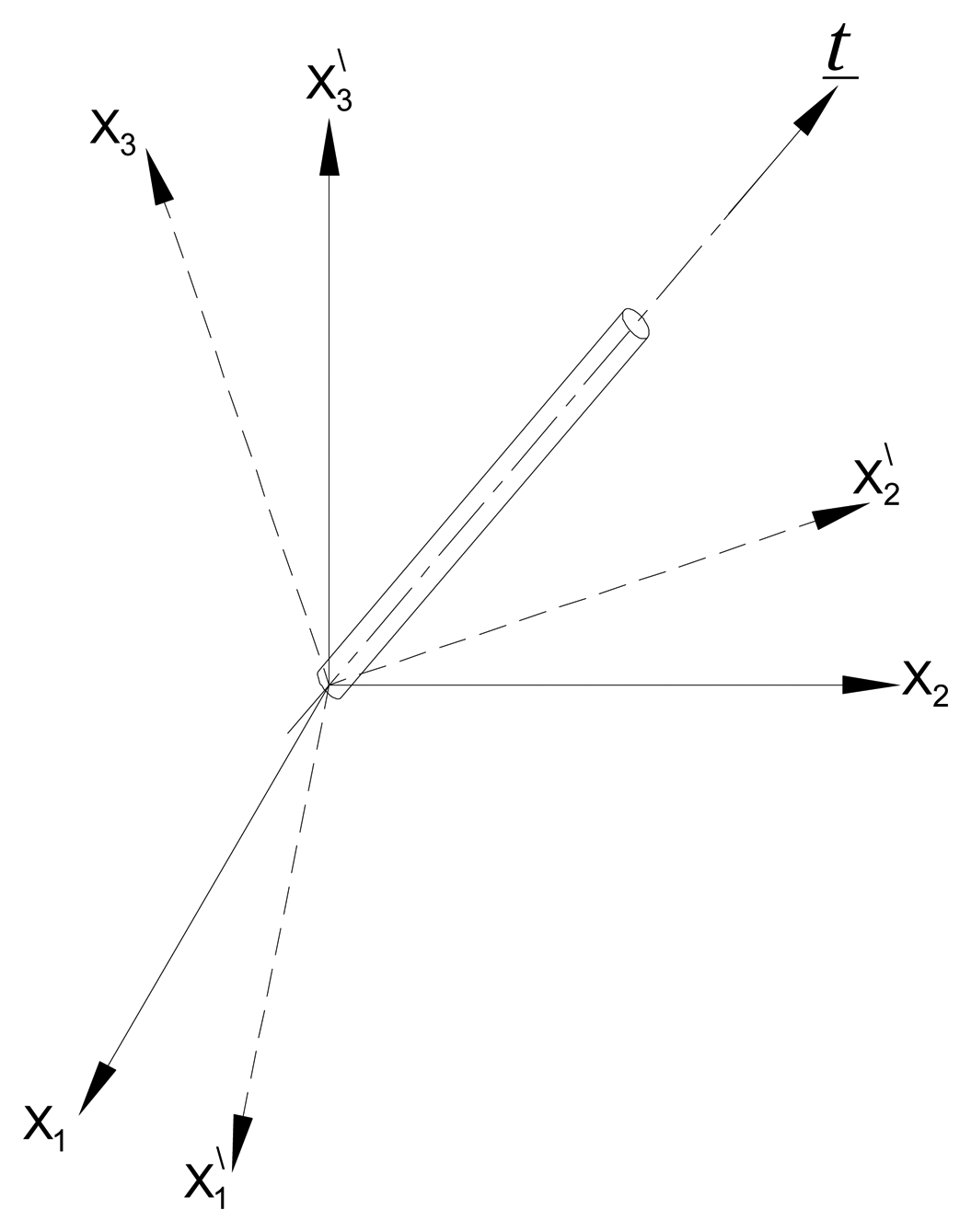
In the case of single crystal silicon filament, which is an anisotropic material, assuming that this filament is initially aligned in arbitrary direction ṯ, that has direction cosines of l, m, n the normalized change in the electrical resistance is given by
where πij, are the components of fourth order piezoresistivity tensor, which characterize the stress-induced resistivity change and T is the difference between the operating temperature (Tw) and the reference temperature (Tref) i.e. (T=Tw−Tref), which linked to temperature coefficients for resistance (α1, α2…). Note that into account that π11=π22=π33, π44=π55=π66 and π12=π13=π23=π21=π31=π32. The same equation can be referred to the off-axis direction cosines l′, m′, n′ as
3. Sensor Noise and Resolution
Generally, mechanical sensors suffer from various noise sources such as thermal, Hooge, shot, photon or thermomechanical [23]. In the case of piezoresistive sensors, the thermal and the Hooge noise sources are found to have high effect on the performance. One of the important performance parameters that are affected by these two types of noise is the sensor resolution, which depends on the total sensor noise and sensitivity. This sensitivity is affected by the sensor dimensions, fabrication parameters, material properties, crystal orientation…etc. In the proposed design, the sensor sensitivity is enhanced by introducing geometrical features in the silicon carrier. In the presented prototyping process flow, p-type dopant is selected since it provides high sensitivity in the [110] direction and its in-plane transverse, which are convenient crystallographic orientations from the fabrication standpoint.
a). Thermal (Johnson) Noise
Johnson noise [23] is fundamental noise in nature for any resistor. This noise is a “white noise” with a spectral density that is independent of frequency, and is considered as the basic performance limit, set by the thermal energy of the carriers in a resistor [24]. Johnson voltage noise power density is given by
For a step dopant profile, the total Johnson noise depends only on geometry and doping level. Electrical resistance can be approximated by [R=ρLR/AR]. The total Johnson noise for a given geometry and doping level (N) is calculated by integrating its power density over the working bandwidth from fmin to fmax yielding
b). Hooge (1/f) Noise
Contrary to Johnson noise, this type of noise is dependent on the frequency; where it dominates at low frequencies due to conductance fluctuations. Furthermore, the flowing current in the device presents a noise that has a power spectral density at low frequency with a divergent behavior. This noise does not appear fundamental in nature and originates from the process variables; therefore, it can be avoided. The fluctuation of 1/f noise in piezoresistive sensors is shown to vary inversely with the total number of carriers (n) in the piezoresistor, as formulated by Hooge [25]. Therefore, while 1/f noise is reduced for heavily doped piezoresistors with deep sections, sensitivity considerations favor lightly doped piezoresistors with shallow sections. Furthermore, an optimal doping concentration is identified to be a function of the piezoresistors' volume and the measurement bandwidth (fmax-fmin) [26]. The annealing conditions are also found to affect the 1/f noise level, with side effect of loss in sensitivity due to dopant diffusion [21]. For a homogeneous resistor, 1/f noise is calculated using Hooge empirical equation as
where α is a dimensionless parameter, which varies depending on the annealing conditions of the implanted piezoresistors. For high doping levels α=1.5×10⁻⁶ [27]. Integrating eqn. (8) from fmin to fmax yields
For a rectangular resistor with constant doping concentration, the total number of carriers can be approximated by the doping density times the doped piezoresistor volume i.e. (n=NLRAR). With this approximation, Hooge noise can be predicted based on the doping level and the piezoresistors' geometry.
c. Sensor Resolution
Using eqn. (11), it is found that εmin is affected by the resistor geometry, temperature, doping level and the sensor sensitivity. The sensor output signal (Vout |total) is composed from two components; the ideal sensor signal at zero noise (Vout) and the sensor noise signal (Vnoise)
4. Sensor Design and Working Principle
The strain sensor presented is designed to operate within a measurement range of 4000 microstrain (με) with a resolution of 1με. These values were selected to cover a wide range of applications that include structural integrity monitoring (crack initiation and propagation) of mechanical and biomedical devices. Figure 1 presents a schematic of the simulated sensor design, which depicts a three-arm sensing rosette. Each sensing arm or unit has four piezoresistors connected in a full-bridge configuration. The sensor chip is composed of single crystal silicon, which has been through various microfabrication processes. The sensor output signal is the resultant of a signal transfer through different structural layers.
The sensing process is initiated from the strained surface that experiences external strain along an arbitrary direction. This surface strain is transferred through the bonding material layer (epoxy in the current case) to the lower surface of the silicon substrate. This transfer process causes some loss in the strain signal strength (first loss) that is dependent on the geometric and material properties of the epoxy layer. To compensate for this signal loss, backside slots have been etched in the bottom surface of the silicon substrate perpendicular to the sensing unit direction, as shown in Figure 1-b. These slots magnify the strength of the transferred strain. The magnified strain is then transferred from the lower surface of the silicon substrate to its upper surface, which results in another loss in its signal strength, (second loss).
When the transferred strain signal reaches the upper surface of the silicon carrier, it is then resolved into three directions (0-45-90°). These directions are the sensing units' orientations, which are designed to solve for the principle stresses. On the upper surface, deep trenches have been etched to compensate for the second signal loss. On each sensing unit, four piezoresistive elements have been prototyped and connected in a full-bridge configuration resulting in a third level of signal magnification. The deformation of the silicon substrate is directly measured from the electrical resistivity change in the form of offset voltage caused by the bridge imbalance. The use of the full-bridge configuration will result in the cancellation of the temperature coefficients of resistance and the local thermal expansion coefficients based on the original values of piezoresistors electrical resistance, which will stabilize the output signal over the operating temperature range.
The four piezoresistors are oriented along the [110] and its in-plane transverse on a (100) p-type silicon. It is reported earlier [28] that when p-type resistors are oriented along these directions, they offer the highest strain sensitivity, which is given by the longitudinal piezoresistive coefficient (πl). However, this value needs to be adjusted to take into account the dependence of πl on doping concentrations [17, 21].
5. Finite Element Simulation
In this paper, a finite element (FE) model has been constructed to simulate the sensor structure using the commercial FE package ANSYS10.0®. The different structural layers have been included starting from the strained surface till the doped regions of the silicon substrate. To verify the feasibility of the designed sensor, four sets of the FE models, shown in Figure 2, have been analyzed. The first set was designed to verify the signal enhancement due to the existence of the geometric features in the silicon carrier e.g. back side slots and front side trenches. The second set of the FE analysis were used to evaluate the sensor performance at different operating temperatures. The third FE simulations set was designed to calculate the contribution of the different noise sources to the sensor output signal. The forth FE simulation set is applied to calculate the designed strain sensor sensitivity and resolution. The strained surface, bonding layer (epoxy), silicon carrier and piezoresistors were modeled using 3-D tetrahedral 10-node elements taking into account the isotropy or the anisotropy of each structural layer.
The FE mesh was refined to ensure a mesh independency with approximately 200,000 degrees of freedom (DOFs), and the load has been applied as a constant displacement on the edges of the silicon carrier. Moreover, the boundary conditions' effect has been isolated by changing the ratio between the silicon carrier dimensions to the strained surface dimensions, fixing the former at the sensing chip dimensions. Furthermore, the effect of changing the fabrication parameters (doping concentration) has been investigated to select the suitable doping concentration. In addition, the effect of temperature change on the material properties' has been investigated. To perform this FE analysis, 3 FE submodels have been built; structural, piezoresistive and coupled-field. In these submodels, the output results were used to calculate the strain induced resistance change, the sensor gauge factor and the expected output signal. Since the values of sensor cross-sensitivity and transverse gauge factor can affect the output signal (introducing a great source of error in the measured strain) an investigation of these factors has also been carried out in the current FE analysis.
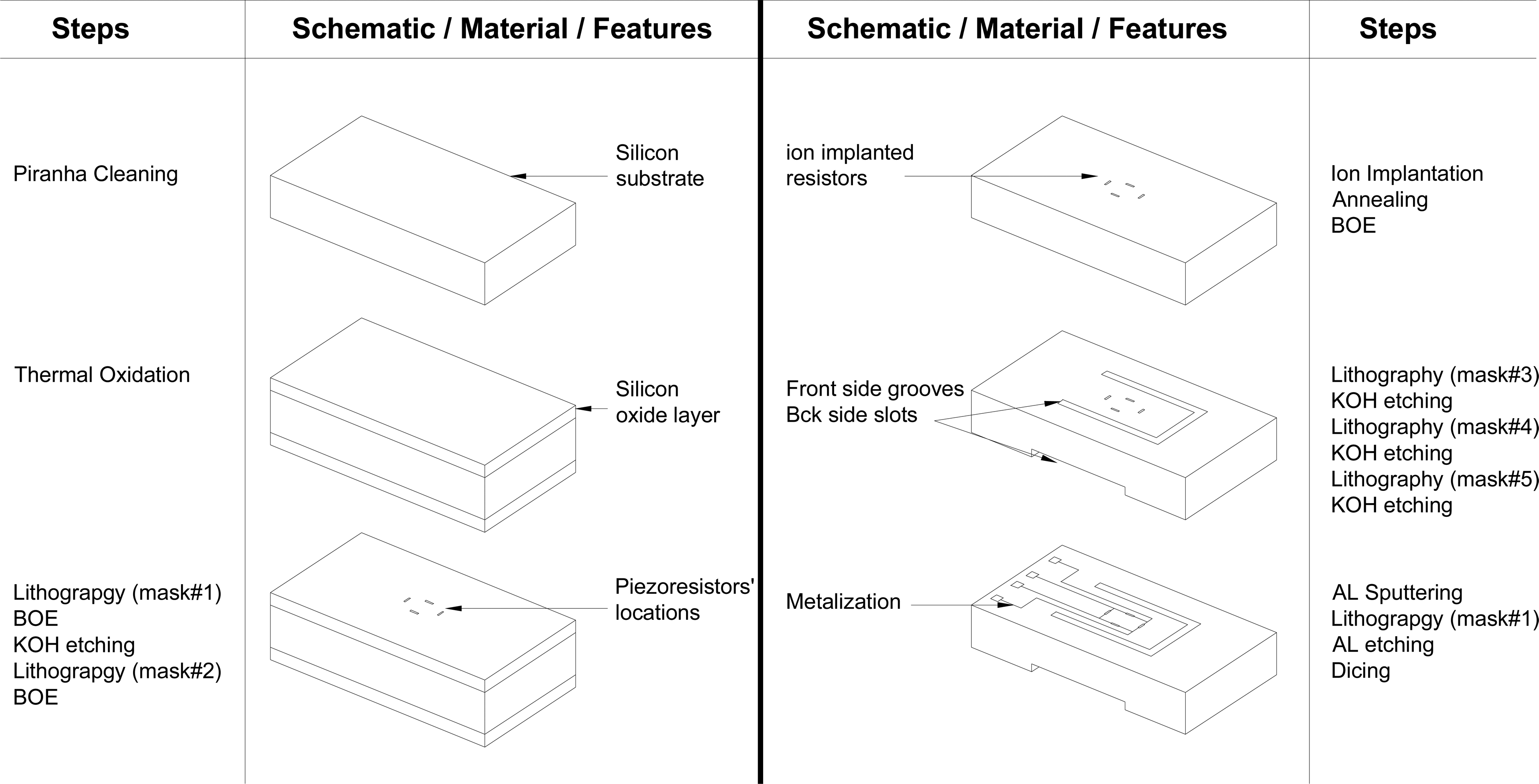
6. Sensor Fabrication
A five-mask microfabrication process flow based on bulk silicon micromachining has been constructed to prototype the proposed MEMS strain sensor. The fabrication process utilizes 4-inch (100) n-type double sided polished silicon substrates with the primary flat along [110] direction. The wafer has thickness of 500±25 μm, bulk resistivity of 10Ω cm and a total thickness variation less than 1μm.
The microfabrication process flow, shown in Figure 3, starts by cleaning the silicon substrates in piranha (3 parts of H2SO4 + 1 part of H2O2). This step is followed by growing 1200 nm of thermal oxide at 1000 °C for 8 hrs in a wet atmosphere of N2. This oxide is intended to serve as the masking layer for the doping process and to minimize silicon lattice damage due to the bombarding ions during the ion-implantation process. Next, a lithography step is performed to pattern the first mask, which defines the surface trenches and the alignment marks in the oxide and the silicon layers. Buffered oxide etch (BOE) and anisotropic etching using KOH are used to pattern the first mask in the silicon substrate.
The second mask is then pattered using two successive steps of lithography and BOE to define the piezoresistors' locations. Boron ion-implantation is then performed according the predetermined specifications from the FE simulation. The intended doping concentration is 5×10¹⁹ atoms/cm3 at a junction depth of 1 μm. The masking oxide layer is then removed by another BOE step. A subsequent annealing step follows the ion implantation process at 1100 °C for about 15 min. An extra wet thermal oxidation step is then performed to grow an insulating oxide layer for one hour at 1000 °C.
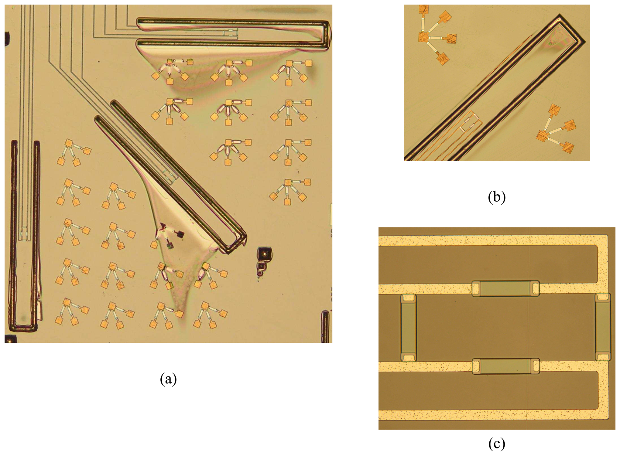
The third mask is used to open via for the aluminum contacts. Aluminum has been sputtered for 30 minutes to get an aluminum layer of thickness 500 nm that will serve in the metallization and interconnects. This aluminum layer is then patterned and etched using aluminum etchant. Finally, lithography, BOE and KOH etching steps are performed to create back side slots. A prototype of the fabricated sensing chip is shown in Figure 4, which contains some characterization structures beside the sensor prototype.
7. Results and Discussion
The typical electrical resistance of the commercial semiconductor strain gauges is 1 kΩ and in metal foil gauges is 120 or 350 Ω. Results from the FE simulation showed that the current design has 15 KΩ/doped piezoresistors. This value can be adjusted (increased or decreased) and tuned based on the microfabrication parameters. Therefore, the proposed sensor design is robust in operating at low-current and low-power applications. The decrease in doping level showed to increase the sensor sensitivity, however it has undesirable effect on the noise level; both 1/f and Johnson.
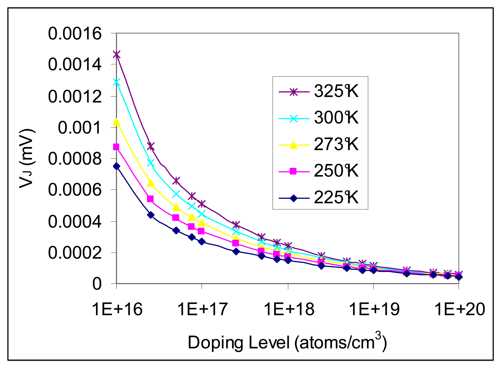
The simulation results have been combined with the analytical modeling to construct the characteristic curves of the MEMS strain sensor. Figures 5 and 6 illustrate the dependence of both Johnson and 1/f noises on the doping concentration at different operating temperatures. Although 1/f noise does not appear to depend on the operating temperature as described in eqn. (9), it is found to follow the same trend as Johnson noise as the doping concentration changes. This trend decreases as doping concentration increases. Due to the nature of Johnson noise as thermal energy fluctuation of the resistors, it is found to increase as the operating temperature increases. This trend is generally correct up to doping level of 1019 atoms/cm3. At this doping level, all the curves tend to coincide and start to be temperature independent. It is noted that increasing the doping level beyond 5×10¹⁸atoms/cm3 reduces the noise dependence on the operating temperature and its absolute value, which improves the sensor performance. In addition, it is clear from Figures 5 and 6 that the value of Johnson noise is lower than the value of 1/f noise by more than two orders of magnitude, which makes the 1/f noise dominating at low frequency range (1 Hz-1 kHz).
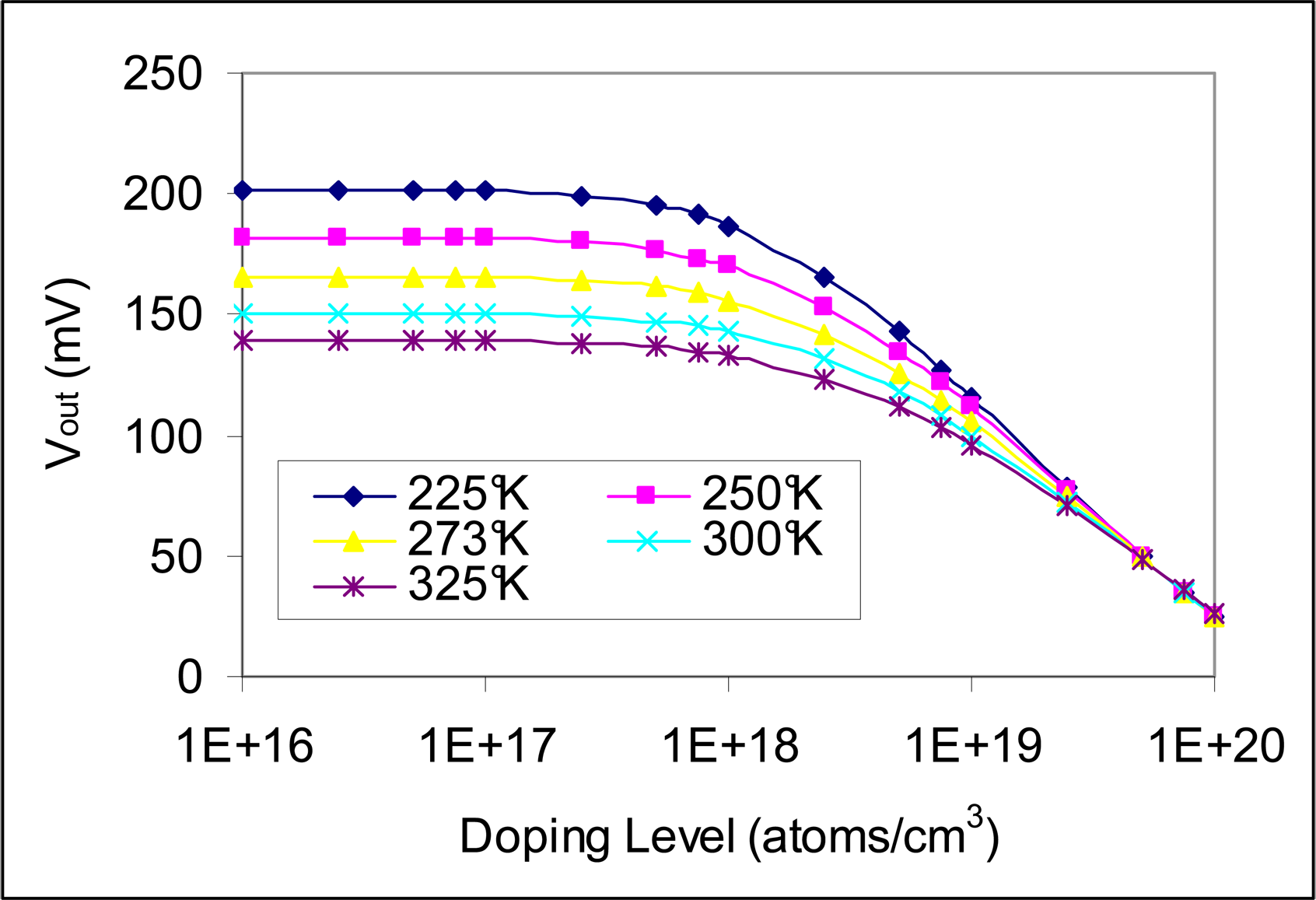
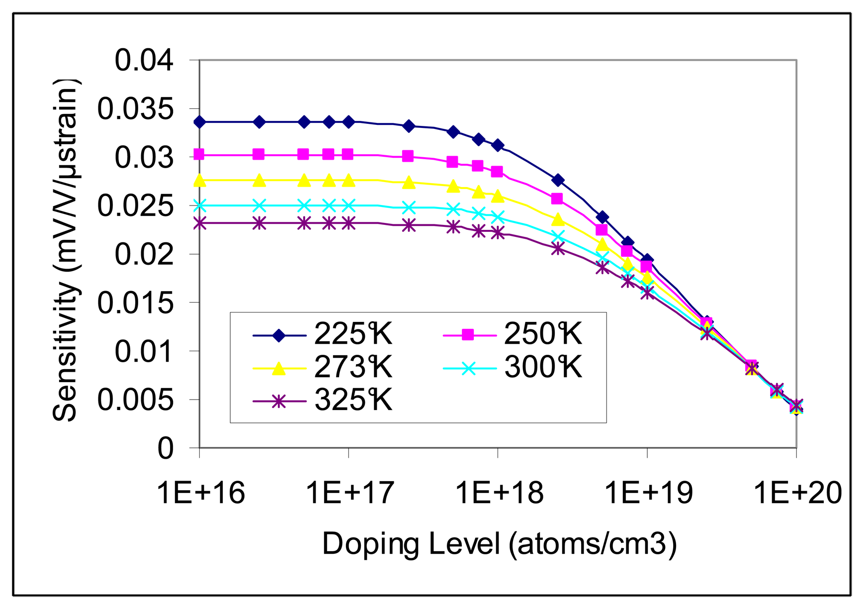
Figures 7 and 8 show both sensor output signal and sensitivity versus doping level at different operating temperatures. It is clear that increasing doping level lowers the output signal and hence reduces the sensitivity. Moreover, working at high doping levels (more than 1019 atoms/cm3) stabilizes the output signal and makes it temperature-independent. Furthermore, high operating temperatures, at doping levels more than 1019 atoms/cm3, reduce the sensor output signal and sensitivity by ∼ 65-75 percent of its original value at low to moderate doping levels (1016-1018 atoms/cm3).
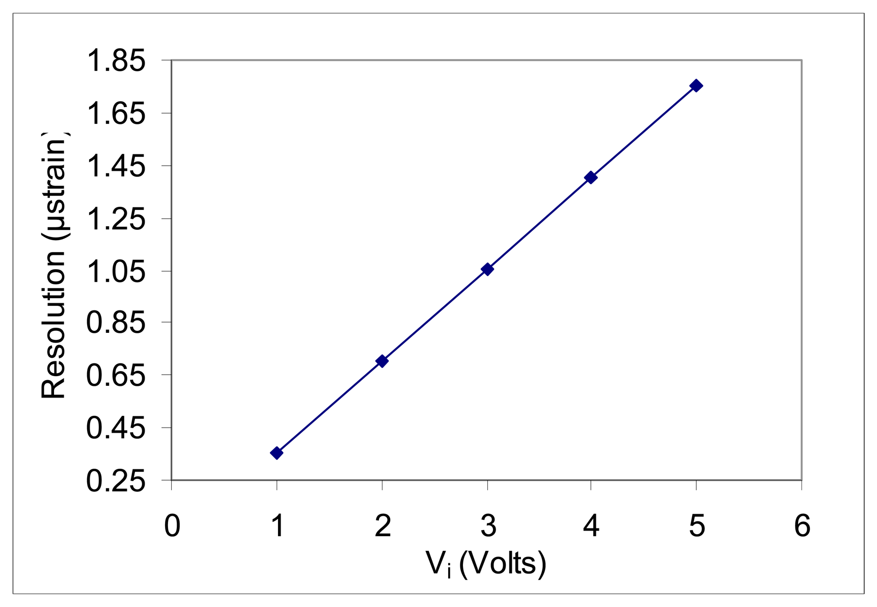
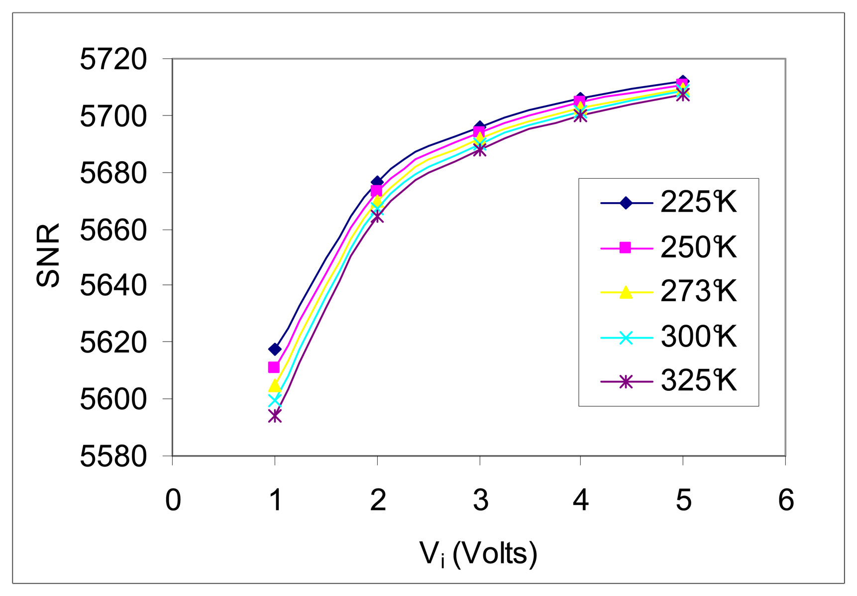
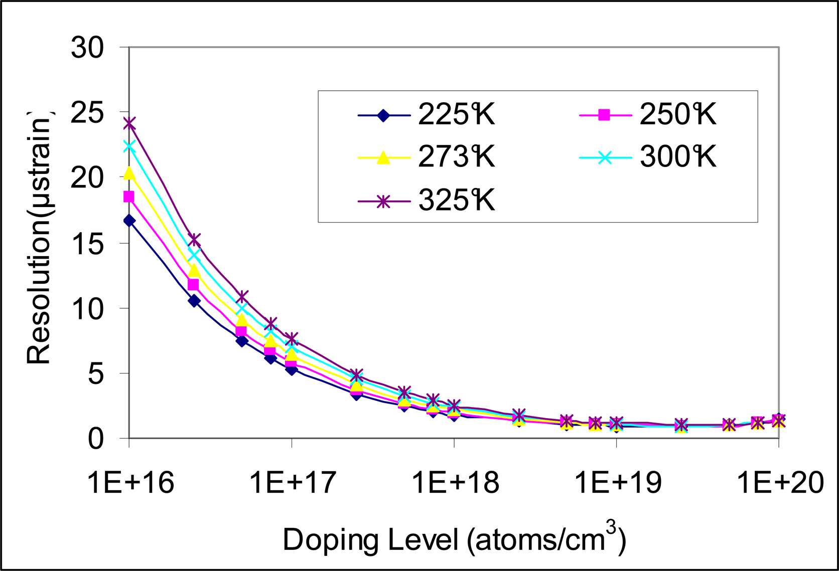
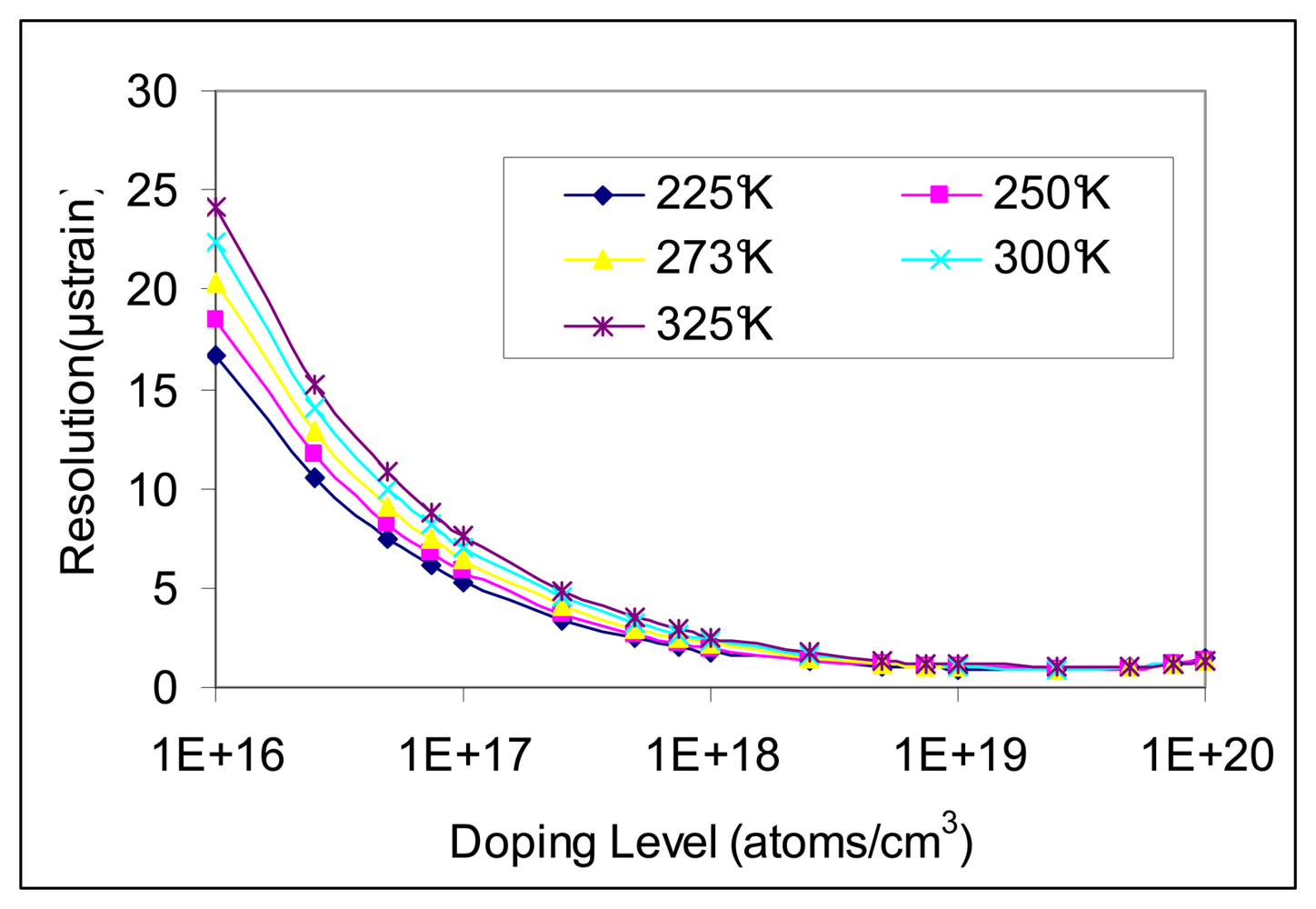
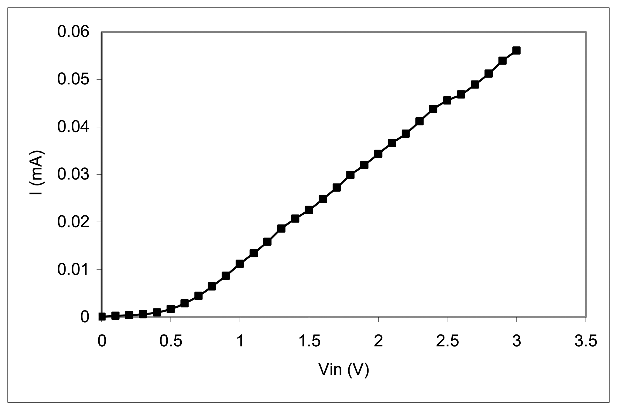
Although sensitivity aspects favor low doping concentrations, the stable sensor resolution shown in Figure 9 requires high doping concentrations (>1019 atoms/cm3), but continuous increase of the doping level will result in a substantial decrease in the sensor sensitivity. The previous argument does not apply to the signal to noise ratio (SNR). To select the proper doping level, the SNR curve, shown in Figure 10, has been constructed. From the SNR results, it is found that doping level of 5×10¹⁹ atoms/cm3 produces the highest SNR with acceptable signal stability over temperature range of ±50 °C (225-325 °K). The sensor input voltage (Vi) is also addressed in the current work. From Figures 11 and 12, it is found that increasing the input voltage increases 1/f noise and SNR. Moreover, sensitivity at this doping level is constant regardless the operating temperature, as shown in Figure 8. However, from the I-V characteristic curve, shown in Figure 13, it is found that a sensor input of ∼1 V and more is sufficient to break the junction. Therefore, input voltage of 3 V has been selected for both the MEMS sensor and the microelectronics in the conditioning circuit.
8. Conclusions
A MEMS piezoresistive strain sensor has been presented. The active sensing material is p-type silicon on a bulk n-type silicon carrier. The sensor is a three-arm rosette that has a temperature self-compensated performance. This sensor is capable of measuring in-plane strains directions, which are the sensing units' orientations. Each sensing unit contains four p-type silicon elements connected in a full-bridge configuration (microbridge) to have some level of signal magnification. These elements are aligned along [110] direction and its in-plane transverse, which are convenient crystallographic orientation from a fabrication standpoint. These directions have the highest gauge factor on (100) plane. This sensor is designed to have high impedance of 15 KΩ, large gauge factor of ∼140 and minimal hysteresis and excellent linearity up to 4000 με. The above values were determined through FE simulation and preliminary results of the fabricated prototypes.
Introducing geometric features in the silicon carrier enhanced the signal strength by more than a factor of three, compared with the unfeatured silicon carrier. Moreover, surface trenches minimized the effect of the sensor cross sensitivity (transverse gauge factor), which contribute to the sensor output signal. Furthermore, the noise sources that are most likely to affect the sensor resolution have been analyzed at different doping levels and operating temperatures.
Doping concentration of 5×10¹⁹ atoms/cm3 has high signal stability over wider temperature range (±50 °C) and the highest SNR. It is proved that the increase in the doping level, up 1019 atoms/cm3, will stabilize the sensor signal and will enhance the SNR. Therefore, an optimum doping concentration based on the sensor design is determined.
Acknowledgments
This work was supported by Alberta Ingenuity Fund, Alberta Provincial CIHR Training Program in Bone and Joint Health, NSERC CRD grant, Canadian Microsystems Corporation (CMC) and Syncrude Canada Ltd.. The authors would like to thank these organizations for their support.
9. Appendix - A: Piezoresistivity Theory
The electronic state of a crystalline anisotropic material depends on the internal atomic structure and the electrons motion in a given crystal orientation. This state forms energy quasi-continua that are called energy bands. The internal atomic arrangement and energy bands can be altered by applying stress (or strain) on the material, resulting in small changes in the electrical conductance in the presence of electric field. This effect is called piezoresistivity, which can be defined as the dependence of electrical resistivity (opposite to conductance) on the applied stress (or strain).
In the case of the semiconducting filament shown in Figure A-1 with electrical resistivity (ρo), length (LR), cross sectional area (AR), and subjected to mechanical strain (ε), the normalized change of the electrical resistance, can be described by:
Utilizing material properties of semiconductors (Δρ/ρo = πσ) [28] and mechanics of materials relations (σ =Yε) [29], eqn. (A1) can be reduced to:
In eqn. (A2), the constant (1+2υ+πY) is called piezoresistive gauge factor (GF). In metallic materials, the geometric term (1+2υ) is dominating; on the other hand, in semiconductors, the piezoresistive term (πY) is more dominating.
A basic axiom in the conduction theory of electric charges is that the Cartesian current density vector components J1, J2, J3 are functions of the Cartesian electric field vector components E1, E2, E3 i.e. Ji=Ji(E1, E2, E3), where i = 1, 2, 3. For ohmic materials, there is proportionality constant for this linear relation, which is the electrical resistivity. Applying the summation implied in the repeated indices, bearing in mind that ρij=ρji yields
Figure A-1.
Semiconductor filament.
In the case of semiconductors, which are anisotropic materials, the piezoresistive effect is dominating the geometrical change of the strained filament. Bridgman [30-32] was the first to experimentally observe this effect in metals under tension and hydrostatic pressure. Experimental observations in semiconductors have followed this work [28, 33-35]. The piezoresistive effect in semiconductors can be described mathematically using the series expansion
where
are the electrical resistivity components for the unstressed conductor and πijkl, Λijklmn… etc. are the components of fourth, sixth and higher order tensors, which characterize the stress-induced resistivity change. For stressed semiconductors, the resistivity components are linearly related to the stress components by:
Combining the above equations, considering the crystal centrosymmetry in silicon and employing the reduced index notation (11→1, 22 →2, 33→3, 13→4, 23→5, 12→6), the electrical resistivity can be described as:
and in an indicial form as:
The governing tensor equation for the conduction of a stressed anisotropic ohmic conductor is obtained by substituting eqn. (A6-b) into eqn. (A3)
Applying this equation in conjunction with eqn. (A6-a) to a stressed cubic crystal (e.g. silicon) yields
These expressions can be further simplified and compacted employing the values of πij in eqn. (6−a) for the silicon crystal and knowing that
and
[28], which reduces eqn. (A8-a) to
These expressions were first presented by Mason and Thurston in 1957 [36]. They are valid only if the coordinate system is aligned with the principle symmetry (unprimed) axes (x1, x2 and x3) of the cubic crystal. For different directions (off-axis coordinate system), which are primed axes in Fig. A-1, coordinate transformation should be applied, producing
Assuming that the filament is initially aligned in arbitrary direction t, that has direction cosines of l, m, n, the current density components are
Similarly, calculating the potential drop, yields
Substituting eqn. (A11) in eqn. (A12) gives the electrical resistance change of a stressed semiconductor filament in eqn. (A13)
but (R=Ro +ΔR) i.e. (ΔR =R-Ro), (Ro =ρoLR/AR). Therefore, (A13-a) reduces to (A13-b)
Putting eqn. (A13-b) in its indicial form yields eqn. (A13-c). This form will ease equations handling and writing, taking into account that π11=π22=π33, π44=π55=π66 and π12=π13=π23=π21=π31=π32
Running the same procedure on the off-axis direction cosines l′, m′, n′ using eqn. (A9), the normalized resistance change will be referred to the off-axis coordinate system by
The effect of temperature change can be considered by adding another term to the above equations accounting for the temperature coefficients for resistance (α1, α2…) as follows
where T is the difference between the operating temperature (Tw) and the reference temperature (Tref) i.e. (T=Tw–Tref). Equation (A15) assumes that geometrical changes and second-order piezoresistivity can be neglected and that the piezoresistive coefficients are independent of temperature, although the last assumption can be removed utilizing the piezoresistance factor [17]. The 36 off-axis piezoresistive coefficients
are related to the three unique on-axis piezoresistive coefficients; π11, π12 and π44 (evaluated in the crystallographic coordinate system) using the transformation in eqn. (A16)
References
- Nagy, M.; Apanius, C.; Siekkinen, J. A user friendly, high-sensitivity strain gauge. Sensors 2001, 18, 20–27. [Google Scholar]
- Hrovat, M.; Belavic, D.; Samardzija, Z.; Holc, J. An investigation of thick-film resistor, fired at different temperatures, for strain sensors. International Spring Seminar on Electronics Technology 2001, 32–36. [Google Scholar]
- Mohammed, A.; Moussa, W.; Lou, E. Mechanical Strain Measurements Using Semiconductor Piezoresistive Material. The 4th IEEE International Conference on MEMS, Nano and Smart Systems, and The 6th IEEE International Workshop on System-on-Chip for Real-Time Applications; 2006; pp. 5–6. [Google Scholar]
- Frazão, O.; Marques, L.; Marques, J.; Baptista, J.; Santos, J. Simple sensing head geometry using fibre Bragg gratings for strain–temperature discrimination. Optics Communications 2007, 279, 68–71. [Google Scholar]
- Li, X.; Zhao, C.; Lin, J.; Yuan, S. The internal strain of three-dimensional braided composites with co-braided FBG sensors. Optics and Lasers in Engineering 2007, 45, 819–826. [Google Scholar]
- Tsuda, H.; Lee, J. Strain and damage monitoring of CFRP in impact loading using a fiber Bragg grating sensor system. Composites Science and Technology 2007, 67, 1353–1361. [Google Scholar]
- Lin, J.; Walsh, K.; Jackson, D.; Aebersold, J.; Crain, M.; Naber, J.; Hnat, W. Development of capacitive pure bending strain sensor for wireless spinal fusion monitoring. Sensors and Actuators A: Physical 2007, 138, 276–287. [Google Scholar]
- Ko, W.; Young, D.; Guo, J.; Suster, M.; Kuo, H.; Chaimanonart, N. A high-performance MEMS capacitive strain sensing system. Sensors and Actuators A: Physical 2007, 133, 272–277. [Google Scholar]
- Hu, N.; Fukunaga, H.; Matsumoto, S.; Yan, B.; Peng, X. An efficient approach for identifying impact force using embedded piezoelectric sensors. International Journal of Impact Engineering 2007, 34, 1258–1271. [Google Scholar]
- Mohammed, A.; Moussa, W. Design and Simulation of Electrostatically Driven Microresonator Using Piezoresistive Elements for Strain Measurements. IEEE Transactions 2005, 103–105. [Google Scholar]
- Cao, L.; Kim, T.; Mantell, S.; Polla, D. Simulation and fabrication of piezoresistive membrane type MEMS strain sensors. Sensors and Actuators A: Physical 2000, 80, 273–279. [Google Scholar]
- Han, B.; Ou, J. Embedded piezoresistive cement-based stress/strain sensor. Sensors and Actuators A: Physical 2007, 138, 294–298. [Google Scholar]
- Suster, M.; Guo, J.; Chaimanonart, N.; Ko, W.; Young, D. A Wireless Strain Sensing Microsystem with External RF Power Source and Two-Channel Data Telemetry Capability. Solid-State Circuits Conference 2007, 380–609. [Google Scholar]
- Wojciechowski, K.; Boser, B.; Pisano, A. A MEMS resonant strain sensor operated in air. The 17th Annual International Conference on Micro Electro Mechanical Systems (IEEE-MEMS); 2004; pp. 841–845. [Google Scholar]
- Mohammed, A.; Moussa, W.; Lou, E. A Novel MEMS Strain Sensor for Structural Health Monitoring Applications under Harsh Environmental Conditions. In The 6th International Workshop on Structural Health Monitoring; 2007; Stanford, CA, USA. [Google Scholar]
- Fraden, J. Handbook of modern sensor: physics, designs, and applications, 2nd ed.; AIP Press-Springer: New York, 1996. [Google Scholar]
- Kanda, Y. A graphical representation of the piezoresistance coefficients in silicon. IEEE Trans. Electron Dev. 1982, 29, 64–70. [Google Scholar]
- Mason, W.; Forst, J.; Tornillo, L. Recent developments in semiconductor strain transducers. 15th Annual Conference of The Instrument Society of America 1962, 110–120. [Google Scholar]
- Kerr, D.; Milnes, A. Piezoresistance of diffused layers in cubic semiconductors. Journal Applied Physics 1963, 34, 727–731. [Google Scholar]
- Tufte, O.; Stelzer, E. Piezoresistive properties of silicon diffused layers. Journal Applied Physics 1963, 34, 313–318. [Google Scholar]
- Harley, J.; Kenny, T. 1/f noise considerations for the design and process optimization of piezoresistive cantilevers. Journal Microelectromechal Systems 2000, 9, 226–235. [Google Scholar]
- Barlian, A.; Park, S.; Mukundan, V.; Pruitt, B. Design and characterization of microfabricated piezoresistive floating element-based shear stress sensors. Sensors and Actuators A: Physical 2007, 134, 77–87. [Google Scholar]
- Bordoni, F. Noise in Sensors. Sensors and Actuators 1990, A21-A23, 17–24. [Google Scholar]
- Johnson, J. Thermal agitation of electricity in conductors. Physical Review 1928, 32, 97–109. [Google Scholar]
- Nyquist, H. Thermal agitation of electric charge in conductors. Physical Review 1928, 32, 110–113. [Google Scholar]
- Hooge, F. 1/f noise is no surface effect. Phys. Lett. A 1969, 29, 139–140. [Google Scholar]
- Vandamme, L.; Oosterhoff, S. Annealing of ion-implanted resistors reduces the 1/f noise. J. Appl. Phys. 1986, 59, 1–74. [Google Scholar]
- Smith, S. Piezoresistance effect in germanium and silicon. Physical Review 1954, 94, 42–49. [Google Scholar]
- Boresi, A. Advanced mechanics of materials, 6th ed.; John Wiley and Sons: New York, 2003. [Google Scholar]
- Bridgman, P. The Effect of Tension on the Electrical Resistance of Certain Abnormal Metals. Proceedings of the American Academy of Arts and Science 1922, 57, 41–66. [Google Scholar]
- Bridgman, P. The Effect of the Transverse and Longitudinal Resistance of Metals. Proceedings of the American Academy of Arts and Science 1925, 60, 423–449. [Google Scholar]
- Bridgman, P. The Effect of Homogeneous Mechanical Stress on the Electrical Resistance of Crystals. Physical Review 1932, 42, 858–863. [Google Scholar]
- Taylor, J. Pressure Dependence of Resistance of Germanium. Physical Review 1950, 90, 919–920. [Google Scholar]
- Bridgman, P. The Effect of the Electrical Resistance of Certain Semiconductors. Proceedings of the American Academy of Arts and Science 1951, 79, 125–179. [Google Scholar]
- Paul, W.; Pearson, G. Pressure Dependence of the Resistivity of Silicon. Physical Review 1955, 98, 1755–1757. [Google Scholar]
- Mason, W.; Thurston, R. Use of Piezoresistive Materials in the Measurement of Displacement, Force, and Torque. Journal Acoustical Society of America 1975, 29, 1096–1101. [Google Scholar]
Figure 1.
A schematic for the proposed MEMS sensor and the design specifications.
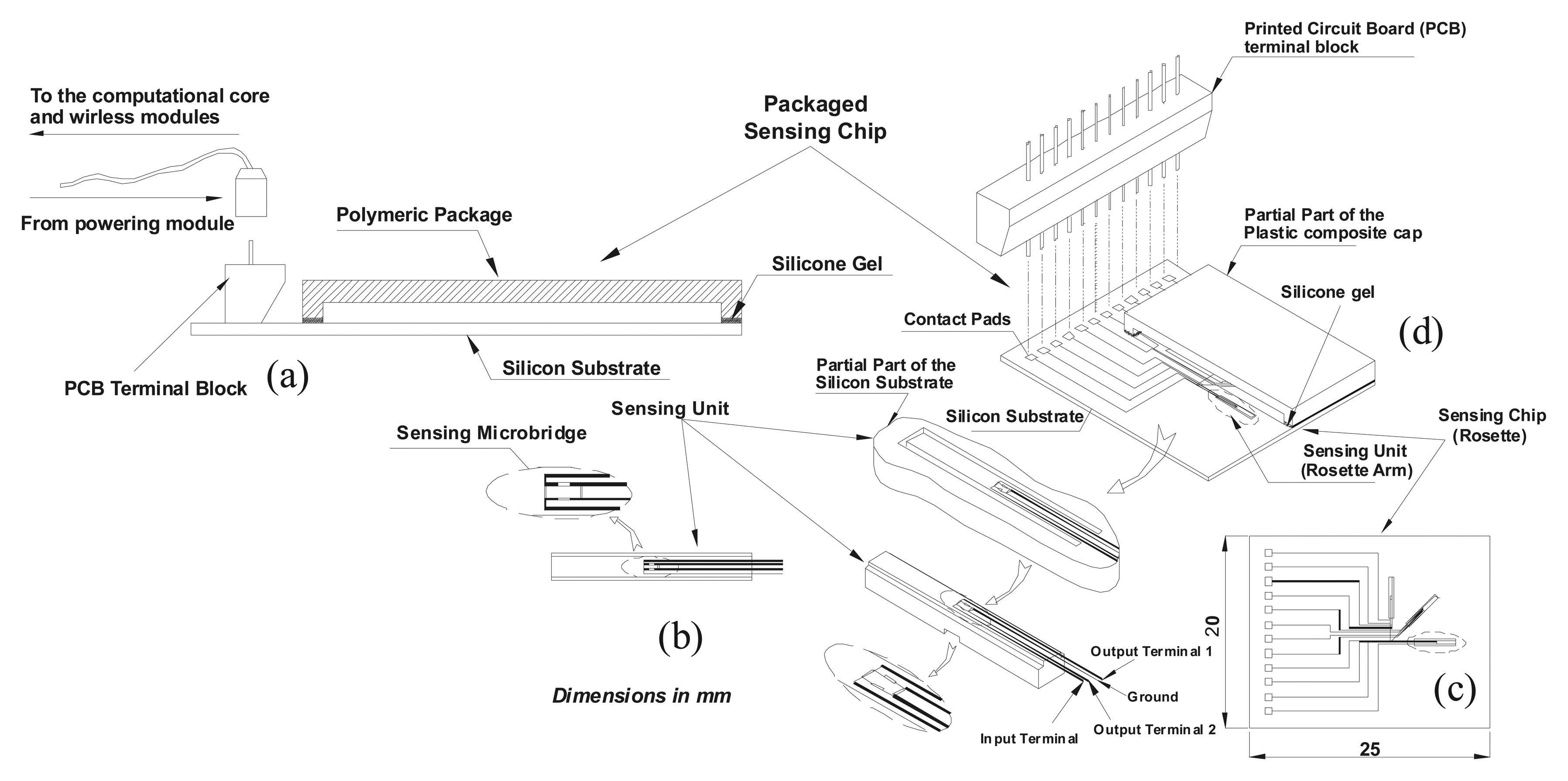
Figure 2.
Details finite element model of the sensing chip.
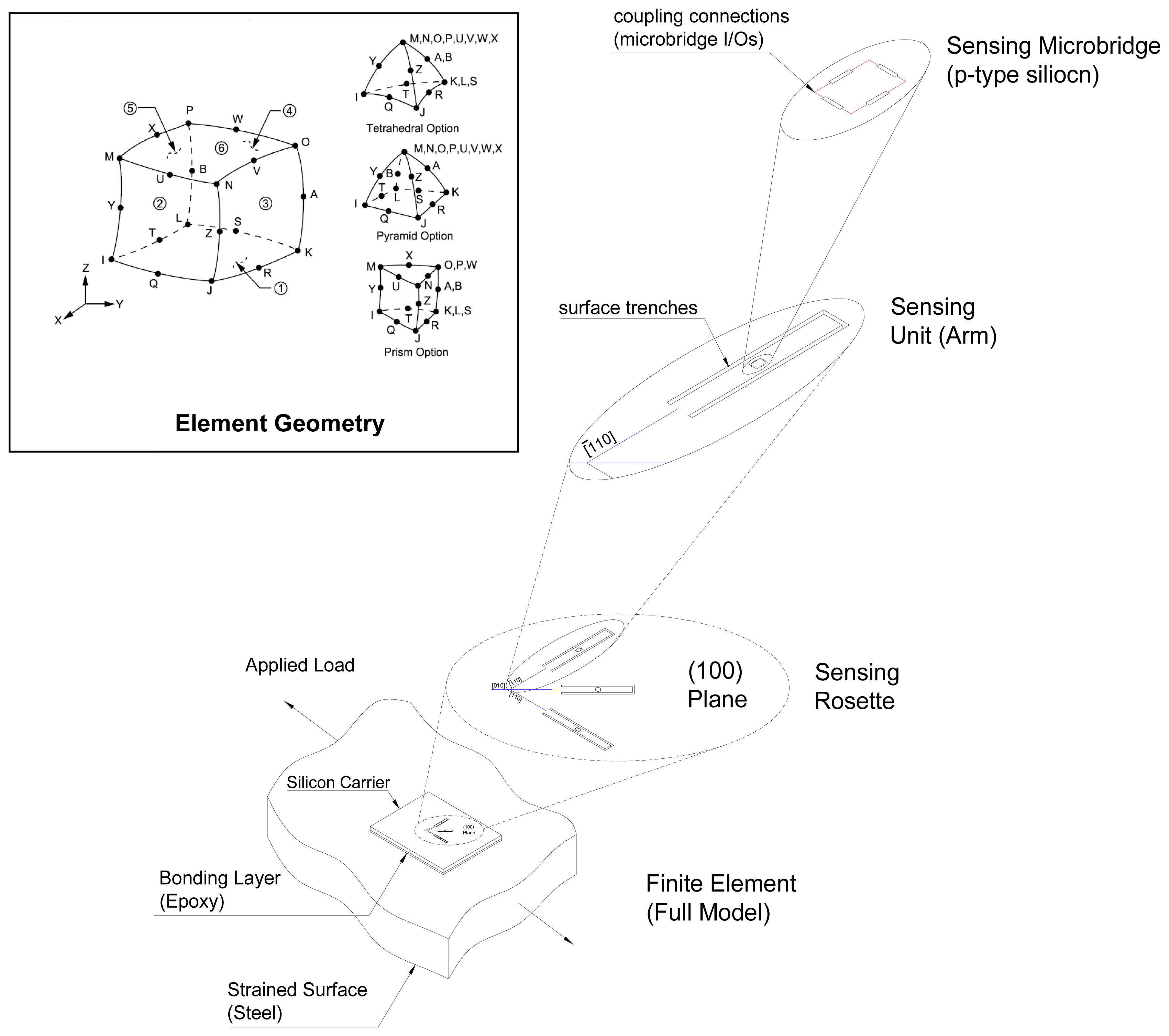
Figure 3.
Proposed microfabrication steps of the sensing unit.
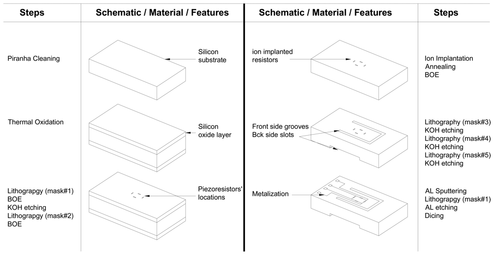
Figure 4.
Fabricated sensing (a) chip, (b) unit and (c) microbridge.

Figure 5.
Johnson noise versus doping level at different operating temperatures.

Figure 6.
1/f noise versus doping level at different operating temperatures for bridge input of 3V.
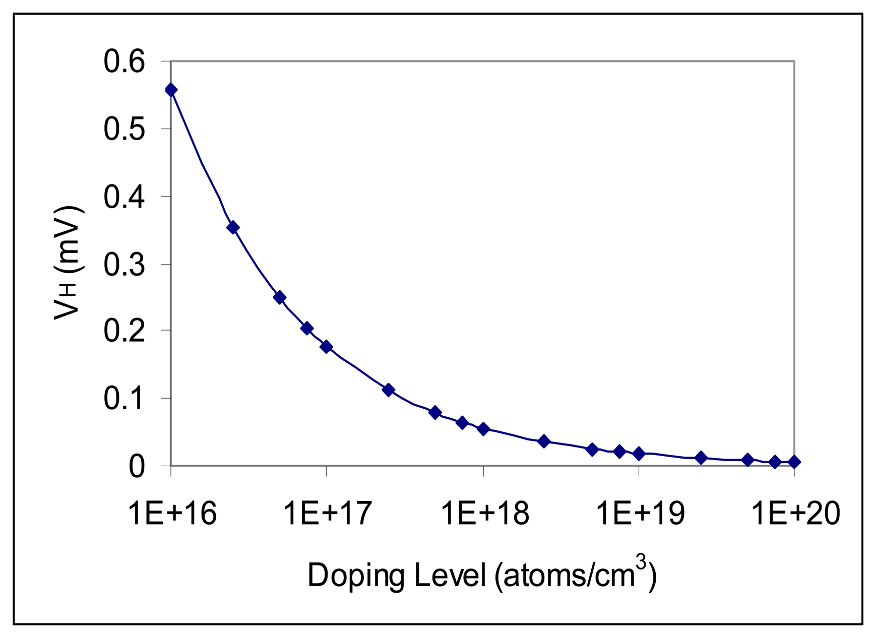
Figure 7.
Sensor output versus doping level at different operating temperatures for bridge input of 3V.
Figure 7.
Sensor output versus doping level at different operating temperatures for bridge input of 3V.
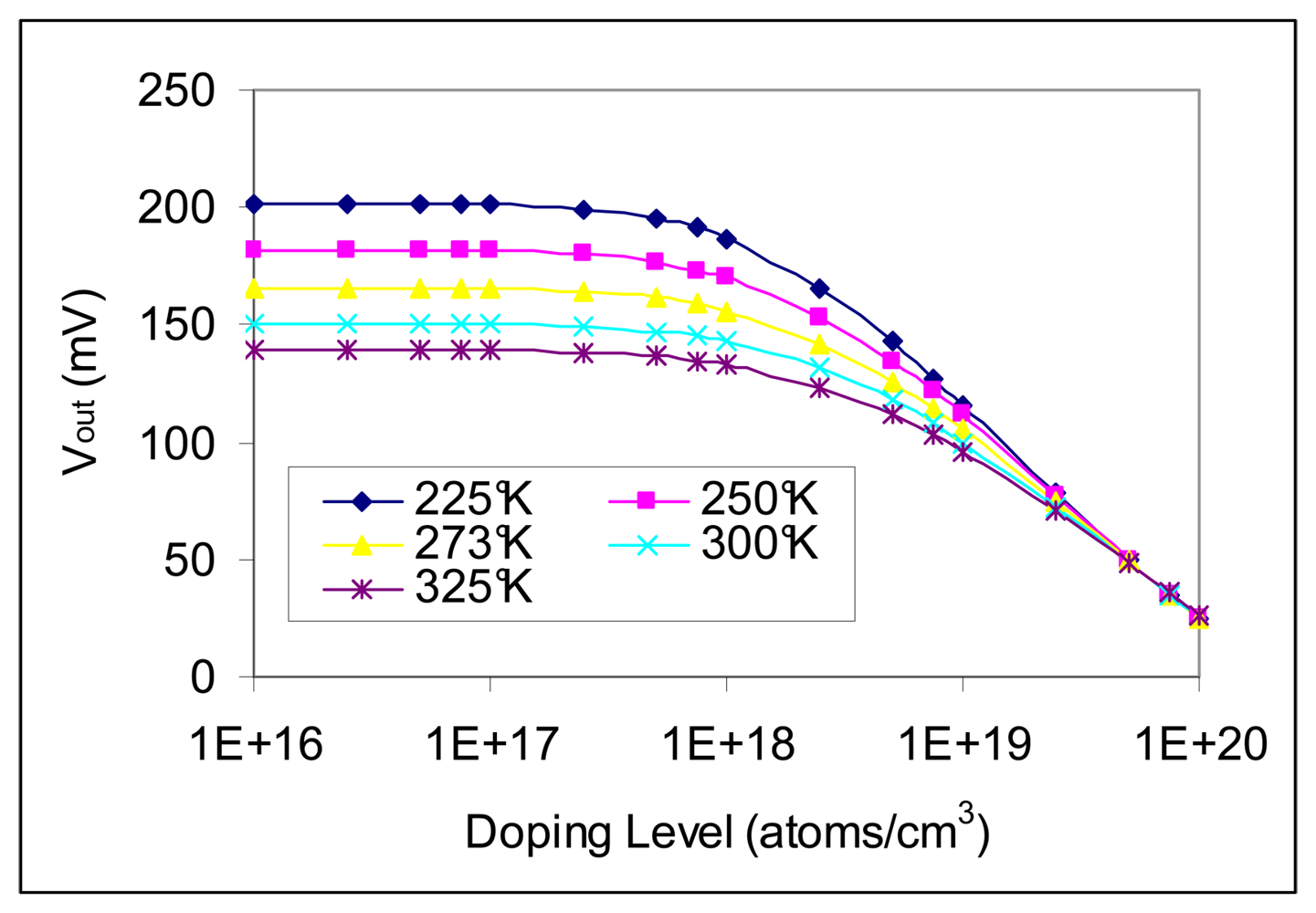
Figure 8.
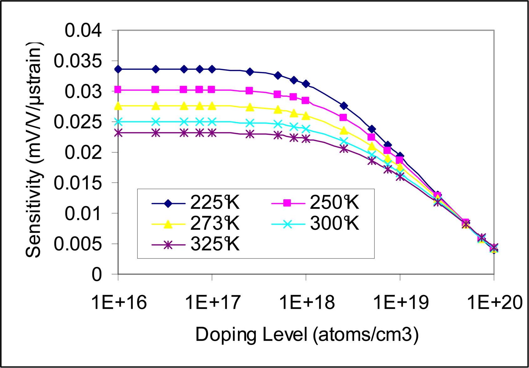
Sensor sensitivity versus doping level at different operating temperatures.
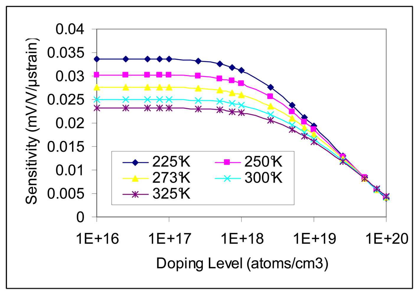
Figure 9.
Sensor resolution versus doping level at different operating temperatures for bridge input of 3V.
Figure 9.
Sensor resolution versus doping level at different operating temperatures for bridge input of 3V.

Figure 10.
Signal to Noise Ratio (SNR) versus doping level at different operating temperatures for bridge input of 3V.
Figure 10.
Signal to Noise Ratio (SNR) versus doping level at different operating temperatures for bridge input of 3V.
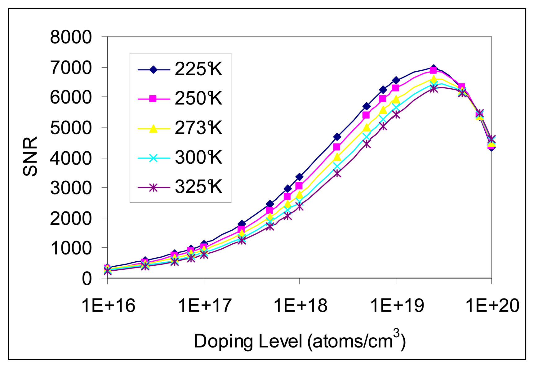
Figure 11.
Sensor resolution dependence on the bridge input for doping level of 5×10¹⁹ atoms/cm3.

Figure 12.
Signal to Noise Ratio (SNR) dependence on the bridge input for doping level of 5×10¹⁹ atoms/cm3 at different temperatures.
Figure 12.
Signal to Noise Ratio (SNR) dependence on the bridge input for doping level of 5×10¹⁹ atoms/cm3 at different temperatures.

Figure 13.
Sensor I-V Characteristic curve.
© 2008 by MDPI (http://www.mdpi.org). Reproduction is permitted for noncommercial purposes.
Share and Cite
MDPI and ACS Style
Mohammed, A.A.S.; Moussa, W.A.; Lou, E. High Sensitivity MEMS Strain Sensor: Design and Simulation. Sensors 2008, 8, 2642-2661. https://doi.org/10.3390/s8042642
AMA Style
Mohammed AAS, Moussa WA, Lou E. High Sensitivity MEMS Strain Sensor: Design and Simulation. Sensors. 2008; 8(4):2642-2661. https://doi.org/10.3390/s8042642
Chicago/Turabian StyleMohammed, Ahmed A. S., Walied A. Moussa, and Edmond Lou. 2008. "High Sensitivity MEMS Strain Sensor: Design and Simulation" Sensors 8, no. 4: 2642-2661. https://doi.org/10.3390/s8042642