CMOS Humidity Sensor System Using Carbon Nitride Film as Sensing Materials

1
Department of Electronic Engineering, Kyungnam University, Masan, Kyungnam 631-701, Korea
2
Electrical Engineering and Computer Science, Case Western Reserve University, Cleveland, Ohio 44106, USA
3
Intel Corporation, Hillsboro, OR 97124, USA
*
Author to whom correspondence should be addressed.
Sensors 2008, 8(4), 2662-2672; https://doi.org/10.3390/s8042662
Submission received: 12 February 2008
/
Accepted: 10 April 2008
/
Published: 14 April 2008
Abstract
:An integrated humidity sensor system with nano-structured carbon nitride film as humidity sensing material is fabricated by a 0.8 μm analog mixed CMOS process. The integrated sensor system consists of differential humidity sensitive field effect transistors (HUSFET), temperature sensor, and operational amplifier. The process contains two poly, two metal and twin well technology. To form CNx film on Si3N4/Si substrate, plasma etching is performed to the gate area as well as trenches. CNx film is deposited by reactive RF magnetron sputtering method and patterned by the lift-off technique. The drain current is proportional to the dielectric constant, and the sensitivity is 2.8 μA/%RH.
1. Introduction
Semiconductor sensors, where semiconductor materials are mainly responsible for the sensor operation and/or semiconductor fabrication processes are applied to sensor fabrication, is an interesting topic to be investigated in terms of the developing miniaturized and high performance sensors. A semiconductor humidity sensor, a typical chemical sensor, is widely used in wide range of measurements and control applications, including those in home appliances, industries, agriculture, hospitals, and laboratories that need greater accuracy and extreme conditions. In order to satisfy a wide range of applications, expected parameters of humidity sensors are sensitivity, response time, reproducibility, long-term stability, selectivity, durability and low cost.
The importance of integrated sensors has been increasingly recognized with the development of technology and science, as miniaturization of sensors offers general advantages with respect to batch fabrication and reduction of cost [1]. However, integrated humidity sensors, using clean semiconductor fabrication process and inorganic materials as sensing materials, have not yet been matured as a commercial product in the global market. Fortunately, several researchers have recently reported some micro humidity sensors, such as a capacitive humidity sensor with on-chip thermal reset [2], a CMOS humidity sensor [3] and a capacitive humidity sensor manufactured by a CMOS-MEMS technique [4], and a company has introduced a new humidity and temperature sensor using CMOS micro-machined chip technology [5]. Humidity sensors have applied the polymer materials with a dip-coating or spin coating method as sensing layer. However, polymer materials can not stand temperature higher than 900 C to make on-chip microsensors on semiconductor substrate, such as silicon. And the polymer layer of the humidity sensors exhibits varying degrees of sensitivity to the same external influences because of hysteresis and swelling. The aging of this layer can also lead to data errors in the humidity signals.
The first study of carbon nitride (CNx) was focused only on synthesizing the stoichiometric β-C3N4 phase, which was suggested as a new super hard material that might have similar or superior hardness and bulk modulus of diamond [6]. However, the stoichiometric β-C3N4 phase was synthesized in 1998 [7]. One of the most significant obstacles to synthesize the stoichiometric β-C3N4 is the hydrogen contamination that can break C-N bonds to N-H and C-H bonds on the films. Hydrogen is usually created by the water molecules that are diffused from the vacuum chamber wall or outside. However, if one could make use of hydrogen defects that were formed intentionally and bonded weakly, carbon nitride would be an attractive candidate material for integrated humidity sensors based on the silicon process [8], because of the high melting point and thermal stability of the carbon nitride films.
In this study, the integrated humidity sensor system with OP amp, using the CNx films as a sensing material, has been designed, simulated, and fabricated based on standard CMOS fabrication process.
2. Design and Fabrication of Integrated Humidity Sensor System
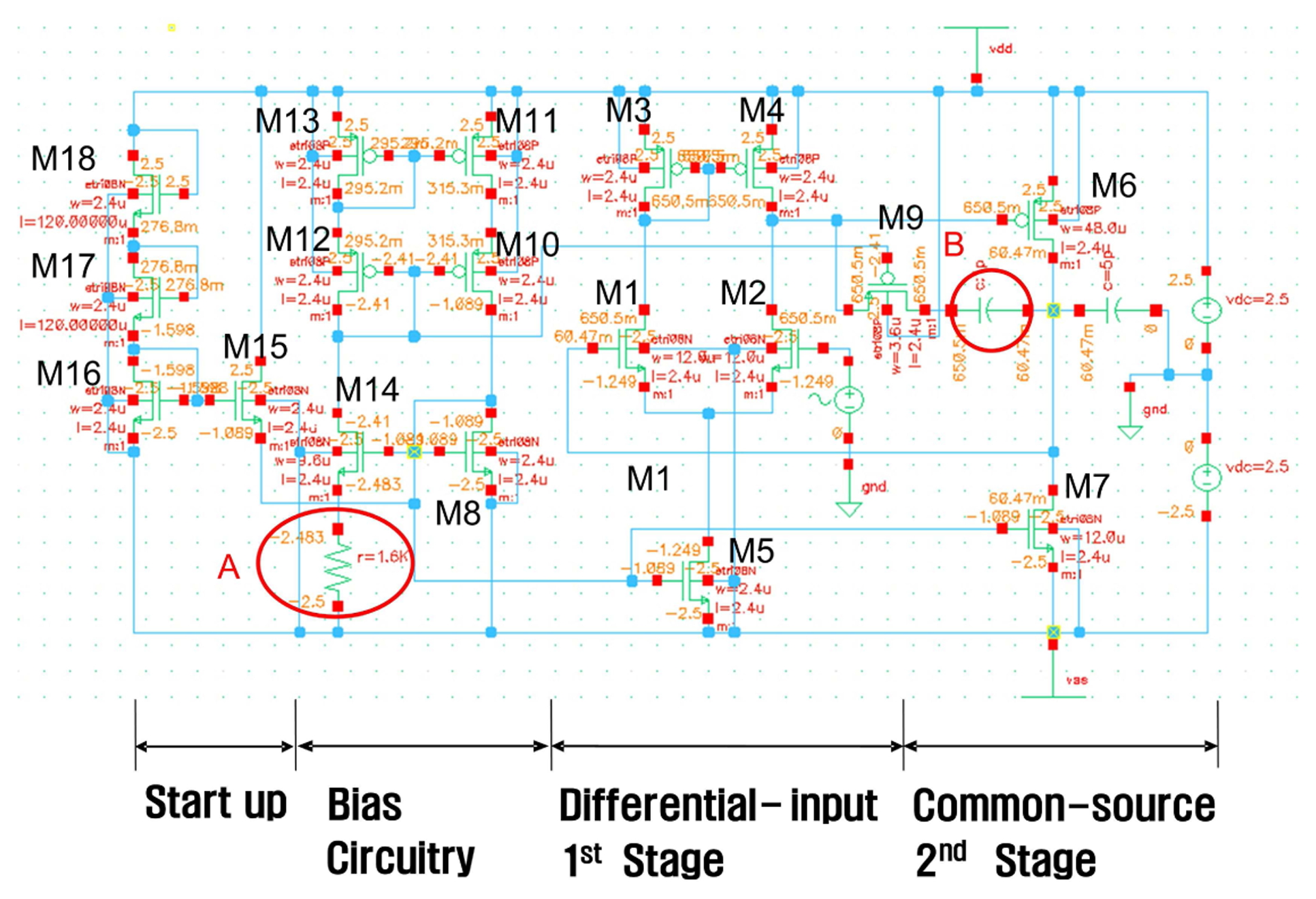
A CMOS humidity sensor system with two stages OP amp is designed by 0.8 μm CMOS technology. It consists of a humidity sensor block, a temperature sensor block and an operational amplifier block for signal amplification and processing in one chip. The two stage operational amplifier has a differential input stage, second gain stage, and output buffer shown in Figure 1. Frequency compensation is necessary for close-loop stability due to a negative-feedback connection. The simplest frequency compensation technique employs the Miller effect by connecting a compensation capacitor Co across the high-gain stage. Due to unintentional feed-forward path through the Miller capacitor, a right-half-plane zero is also created and the phase margin is degraded. Such a zero, however, can be removed if a proper nullifying resistor in inserted in series with the Miller capacitor [9, 10].
The NMOSFET M1 and M2 provide the input differential pair, and the PMOSFET M3 and M4 provide the active load, respectively in Figure 1. The differential input stage is biased by the current mirror M5 and M8, in which the reference current is determined by the internal resistor connected with an adjustable external resistor (circle A). The second stage which means the output stage consists of the common source-connected NMOSFET M7. Transistor M8 provides the bias current for M7 and acts as the active load. An internal compensation capacitor (circle B) and transistor M9 are included for stability. A bias circuit is determined with a stable transconductance which is matched to the conductance of a bias resistor. Therefore, the transistor transconductances are not dependent on the power-supply voltage, as well as the process parameters and the temperature variations. To prevent the zero-current state in the bias circuit, a start-up circuit is included.
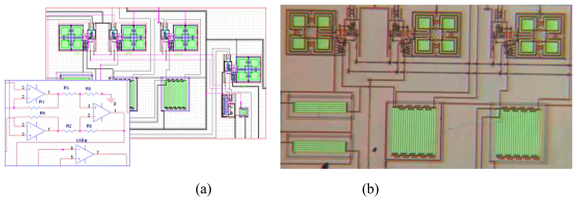
The layout of the operational amplifier is shown in Figure 2. Each function block in the operational amplifier are separated by well and metal guard rings. Input lines are given to twisted pair by two metal layers because it is a particularly effective and simple way of reducing both magnetic and capacitive interference pickup. Twisting the wires tends to ensure a homogeneous distribution of capacitances. Feedback capacitance of 5 pF is designed near to amp block. The common centroid placement design and dummy poly rings are employed for reducing the mismatch from over etching and electrical noses. Input FETs of the differential operational amplifier are placed also taking into consideration operational matching between halves of the cell layout.
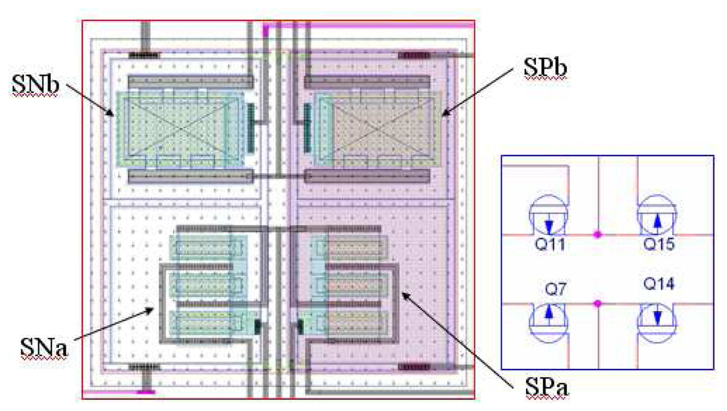
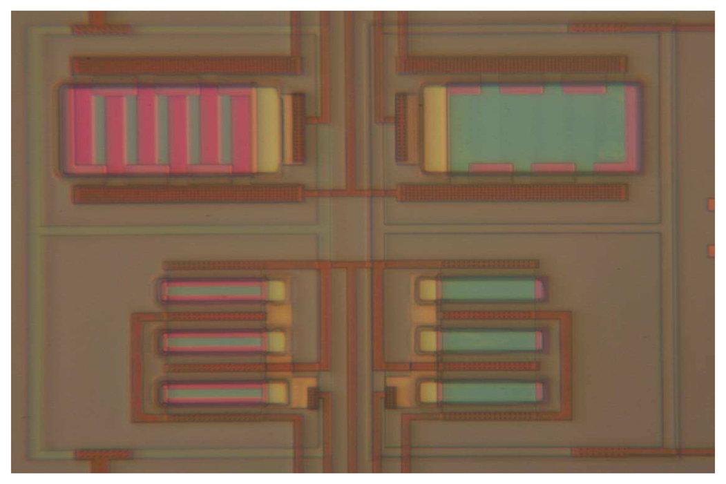
Figure 3 shows the design of a four humidity sensitive field effect transistors (HUSFETs): SPa, SPb, SNa, and SNb. The middle letter, ‘P’ or ‘N’ means the channel type of the FET sensor and the last letter ‘a’ or ‘b’ is the type of the sensor structure. The type ‘a’ is a multi-finger gate MISFET structure with 60×3/8 W/L ratio, and ‘b’ is an interdigitated source-drain MISFETs with (60×5/8) W/L ratio, which are covered with gate electrode. Through the parallel connection of SNa and SPa, these two HUSFETs operate as a single HUSFET with a width equal to the sum of the individual transistor width, having a same length. The drain and source areas can be shared with adjacent HUSFETs. Two benefits are achieved with this layout: (1) smaller layout size and (2) the reduction of the depletion capacitances in source and drain. The reduction of depletion capacitance plays an important role of the protection of latch-up in analog design or in output driver design. No latch-up was found in this sensor system. Figure 4 is a metallurgical microscope image of the sensor block in a fabricated chip.
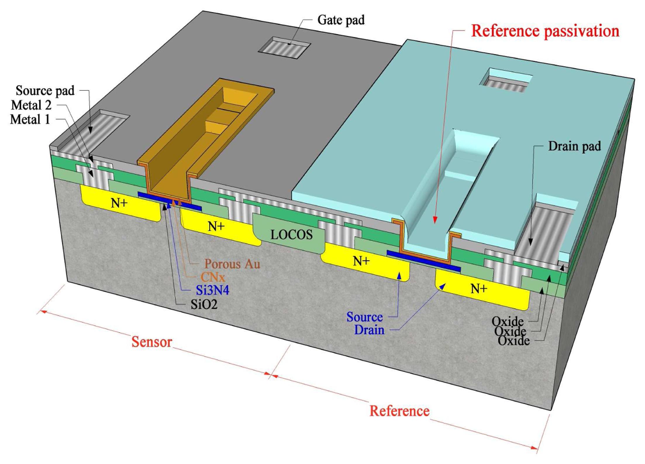
A differential HUSFET has a pair of transistors, a sensing transistor (denoted ‘S’) and a reference transistor (denoted R), as shown in Figure 5. A reference transistor is applied to eliminate the effect of unwanted factors, temperature, other gases, electrical noises, etc. The differential signal from sensor and reference is transmitted to the amplifier block. The fabrication is based on 0.8 μm CMOS technology which contains two poly, two metal and twin well process. Some steps for sensing area of HUSFET are added in the conventional CMOS process. For the formation of CNx film on the gate layer, the plasma etching is performed to each gate along with trench. CNx film is deposited by a reactive RF magnetron sputtering system with DC bias and patterned by the lift-off technique. To fulfill the requirement of differential sensor, water permeable gold layer is deposited only on the gate region of the sensing transistor. After that, the photo resist is coated on the gold pattern with a mask. The photo resist for passivation is patterned on the gate area of reference FETs to protect the reaction with water vapor.
3. Results and Discussion
AC response of open loop gain in the operational amplifier is expressed as:
where, Ao is a low-frequency open-loop gain and fPD is a dominant-pole frequency. The unity-gain bandwidth is written as
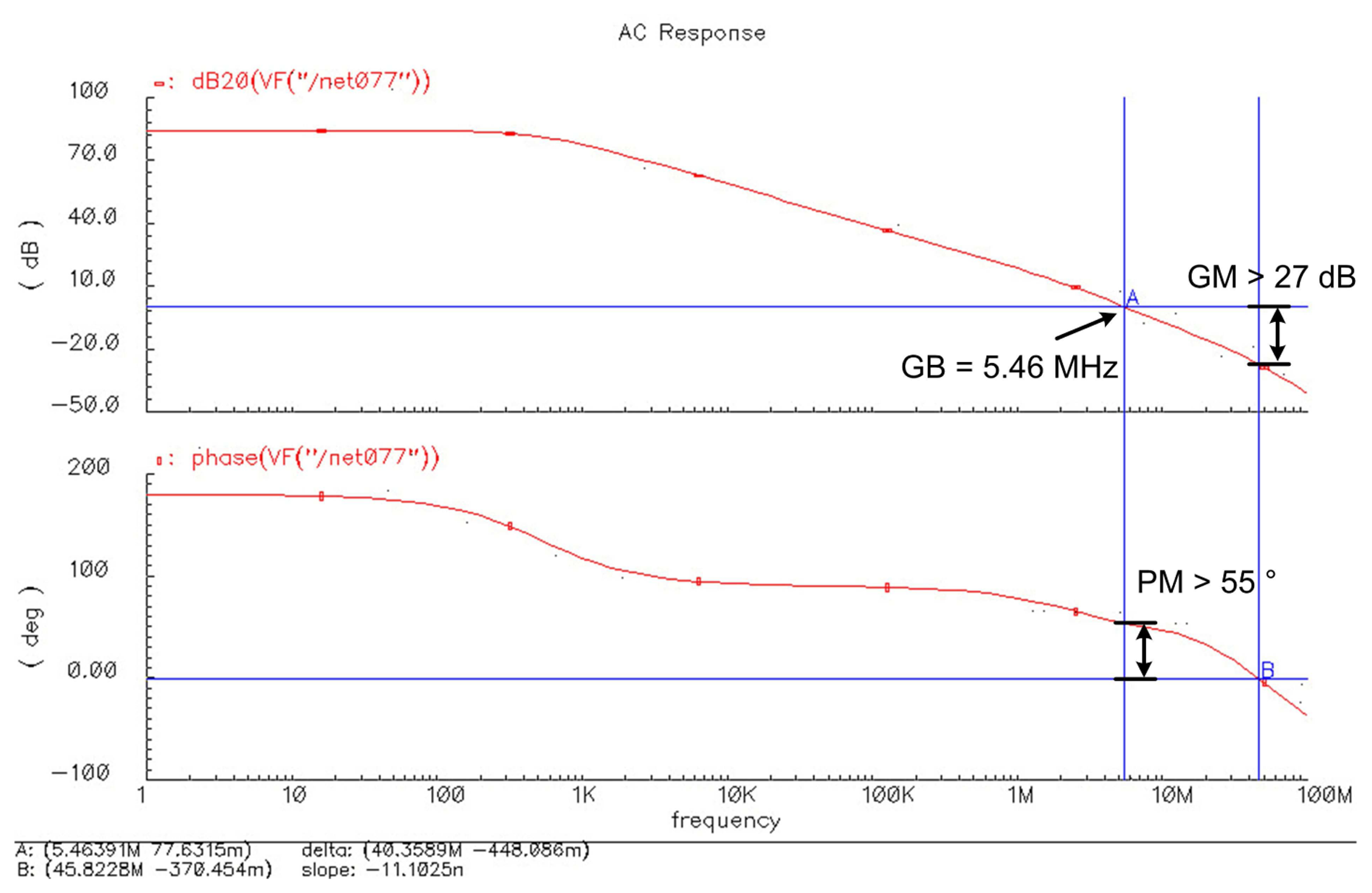
and is also called the gain-bandwidth product. The open loop gain Ao is about 85 dB and the dominant-pole frequency fPD is about 140 Hz shown in Figure 6. The unity-gain bandwidth fT (about 10 MHz) can be obtained at around 1 dB in Figure 6. Its value is a little bit higher than the calculated one from equation (2).
Phase margin and gain margin that are easily evaluated from the Bode diagram are used for a main criterion of frequency response stability. The phase margin PM is the amount of additional phase lag at the gain crossover frequency required to bring the system to the verge of stability, and the gain margin (GM) is the reciprocal of the magnitude |G(jw)|at the frequency at which the phase angle is -180°. The GM is positive if it is more than unity and negative if less than unity. The positive GM (in decibels) means that the system is stable and the negative GM means the opposite. For satisfactory performance of the sensor system, the PM should be between 30° and 60°, and the GM should be greater than 6 dB. In Figure 7, the GM is about 27 dB and the PM is about 55°, respectively.
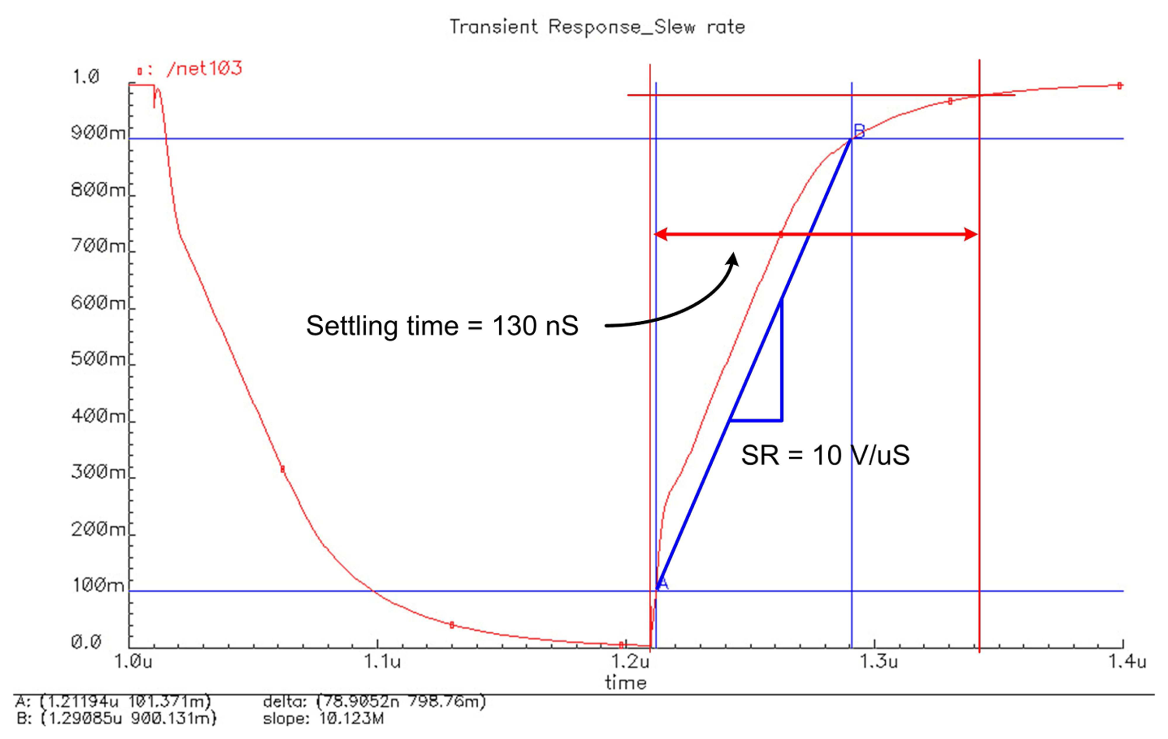
The maximum rate of change of the output voltage is the slew rate SR of the operational amplifier, the unit of which is usually given as volts per microsecond and written as
where, Vo is a output voltage, Cc is a compensation capacitor, and Iq is a bias current. Although the rate of change in output voltage can be either positive or negative, the SR is defined as a positive quantity. The settling time is the time that output is settled to within ± 0.1% of its final value, when the operational amplifier is connected as a unit-gain follower and step voltage 1 V is applied at the input. From Figure 8, it shows that the SR is 10 V/uS and the settling time is 130 nS under 5 pF load capacitor.
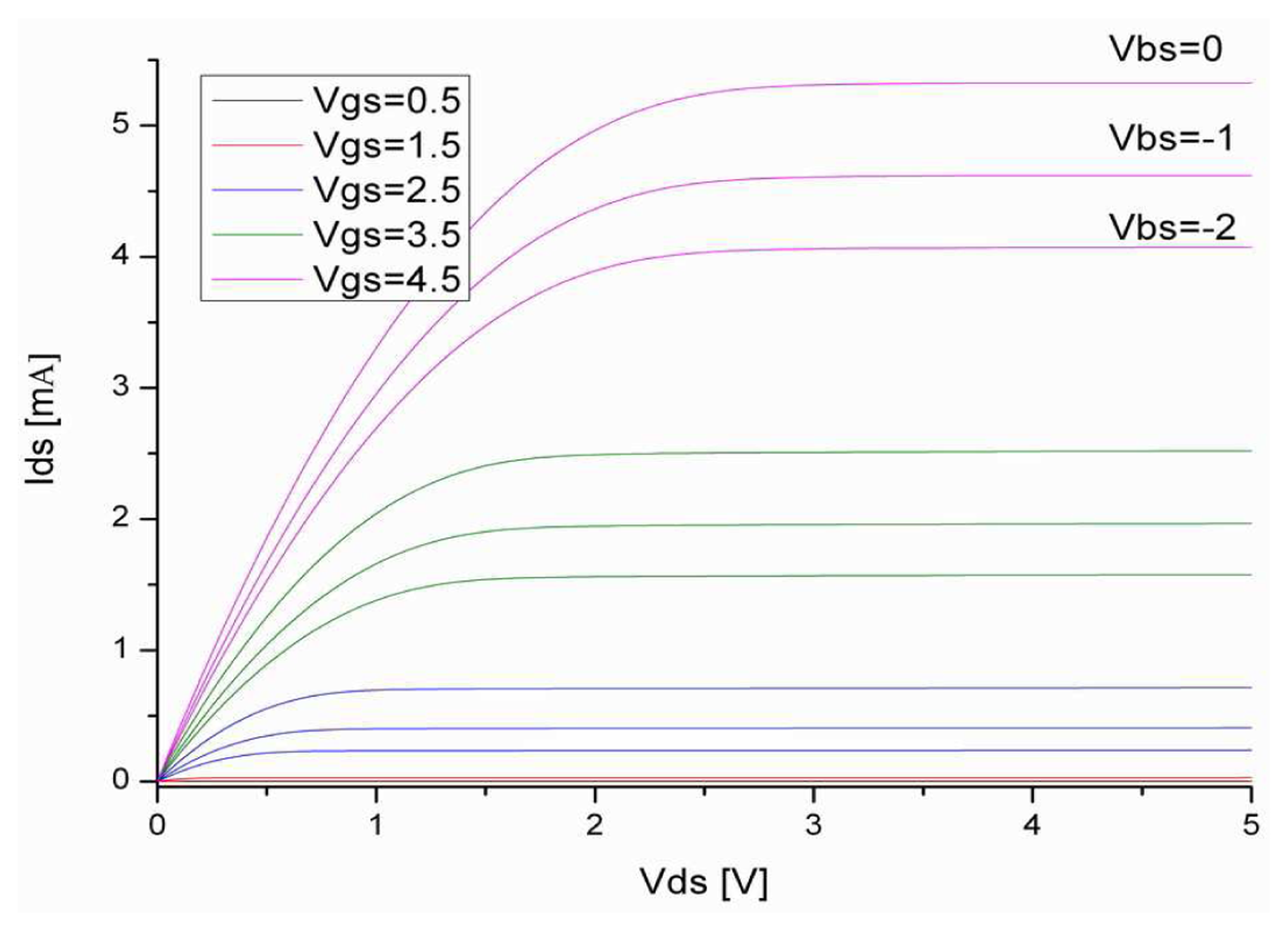
The electrical characteristics of the fabricated CMOS transistors and HUSFETs are measured by a semiconductor test and analyzer (CATS CA-EDA) and C-V plotter (HP 4280A) in self-designed measurement chamber. To avoid condensation of water vapor on chamber wall or pipelines, caused by the different temperature between input vapor and chamber inside, the devices and reference sensors put together in the constant-temperature chamber controlled by PID. Figure 9 shows the current-voltage characteristics of nMOSFET with substrate bias. The poly-nitride etch stop process is applied to nMOSFET and HUSFET both. However, HUSFET has the humidity sensing layer (CNx film) in gate and NMOSFET has not. NMOSFET with 180/80 aspect ratio presents a typical MOSFET curves as much as the conventional MOSFET, as shown in Figure 9. As would be expected, the added poly-nitride etch stop process for the sensing area on the gate does not noticeably affect the original CMOS process.
The threshold voltage of HUSFET is given as [11]
where ψ 'MS is the work function difference between the gate metal and substrate material, Qss is the charge density of the fixed surface state, Qi is the effective interface charge density, Qd is the charge density per unit area in depletion region and ψ F is the Fermi potential of the substrate. The porous Au electrode is deposited on the structure of C3N4/Si3N4/SiO2/Si in HUSFET gate layer, as shown in Fig. 10. The capacitance per unit area at inversion state, Ci', can be expressed as [12]
and
where Csi, Cox, Csn and Ccn are the capacitance of unit area in depletion region of substrate, SiO2, Si3N4 and C3N4, respectively, and dcn is the thickness of carbon nitride film, ε o is the relative permittivity of free space and ε cn is the relative permittivity of CNx film. When hygroscopic CNx film is exposed to water molecular, the modified dielectric constant can be written by Looyenga's empirical equation [13]
where γ is the fractional volume of water in the carbon nitride film and ε w is the dielectric constant of water given by [14]
where T is temperature in Kevin. Shibata et al. have reported the calculated γ in a polyimide film [15].
The humidity sensing properties of an n-channel HUSFET (SNa) is shown in Figure 11. When the ambient temperature is 25 °C and the relative humidity is 20%, the threshold voltage of the n-channel HUSFET (SNa) is about -11.1V at Vsb = 0V.
This value is in good agreement with the calculated value that was achieved from Equation (4). The threshold voltage of nHUSFET is much lower than that of nMOSFET, because the Ci' is reduced and the interface charge density Qi is increased due to the deposition of carbon nitride. When the relative humidity increases from 20 %RH to 70 %RH, the drain current of the SNa increases from 0.85 to 0.99 mA at Vgs = -9.0V and T=25°C. When water molecules meet carbon nitride layer through the porous gold layer of HUSFET gate, they are chemisorbed on the available sites of the carbon nitride surface by dissociative mechanism to form two hydroxyl ions for each water molecule, which possess a high local charge density and a strong electrostatic field, and the proton reacts with an adjacent surface O2- group to form a second OH- group. Therefore, singly bonded water molecules are able to form dipole and to reorient freely under an externally applied gate field, resulting in an increase in the dielectric constant. This is also attributed to the threshold voltage and the drain current changes of HUSFET.
Figure 12 shows the relationship between the drain current and the relative humidity of nHUSFET. The gate voltage and the source-drain voltage are fixed at Vgs = -9.0 V and Vds = 4 V. If a sensitivity is defined as S=dID/dRH, then the sensitivity of the SNa is 2.8 μA/%RH.
4. Conclusions
The integrated micro humidity sensor system, using CNx films as the sensing material, has been designed and fabricated with an operational amplifier based readout circuit. The poly-nitride etch stop process has been tried to form the sensing area in a standard CMOS process. The operational amplifier revealed the stable operation for the signal processing of sensor part, so that unity gain bandwidth was more than 5.46 MHz and slew rate was more than 10 V/uS, respectively. The drain current of the n-channel HUSFET increased from 0.85 to 0.99 mA as the relative humidity increased from 20 to 70 %RH. The integrated micro humidity sensor system showed the sensitivity of 2.8 μA/%RH at constant drain and gate bias.
Acknowledgments
This research was financially supported by the Ministry of Commerce Industry and Energy (MOCIE), and Korean Industrial Technology Foundation (KOTEF) through the Human Resource Training Project for Regional Innovation.
References and Notes
- Rittersma, Z. Recent achievement in miniaturized humidity sensors – a review of transduction techniques. Sensors and Actuators A 2002, 96, 196–210. [Google Scholar]
- Kang, U.; Wise, K. D. A high –speed capacitive humidity sensor with on-chip thermal reset. IEEE Trans Electron Devices 2000, ED-47, 702–710. [Google Scholar]
- Qiu, Y.Y.; Azeredo-Leme, C.; Alcacer, L.R.; Franca, J.E. A CMOS humidity sensor with on-chip calibration. Sensors and Actuators A 2001, 92, 80–87. [Google Scholar]
- Dai, C.L. A capacitive humidity sensor integrated with micro heater and ring oscillator circuit fabricated by CMOS-MEMS technique. Sensors and Actuators B 2007, 122, 375–380. [Google Scholar]
- www.sensorland.com/Homepage047.html.
- Liu, A.Y.; Cohen, M.L. Prediction of new low compressibility solid. Science 1989, 245, 841–842. [Google Scholar]
- Chowdhury, A.K.M.S.; Cameron, D.C.; Hashmi, M.S.J. Vibrational properties of carbon nitride films by Raman spectroscopy. Thin Solid Film 1998, 332, 62–68. [Google Scholar]
- Lee, J.G.; Lee, S.P. Humidity sensing properties of CNx film by RF magnetron sputtering system. Sensors and Actuators B 2005, 108, 450–454. [Google Scholar]
- Palmisano, G.; Paumbo, G. A compensation strategy for two-stage CMOS opamps based on current buffer. IEEE Trans. Circuit Syst. I Fundam. Theory Apply 1997, 44, 257–262. [Google Scholar]
- Allen, P. E.; Holberg, E. D. R. CMOS analog circuit design 2nded.; Oxford: Oxford, 2002; pp. 140–148. [Google Scholar]
- Richman, P. MOS Field-Effect Transistors and Integrated Circuit; Wiley: New York, 1973; p. 31. [Google Scholar]
- Lee, S.P.; Park, K.J. Humidity sensitive field effect transistors. Sensors and Actuators B 1996, 35-36, 80–84. [Google Scholar]
- Schubert, D.L.; Nevin, J.H. A polyimide-based capacitive humidity sensor. IEEE Trans Electron Devices 1985, ED-32, 1220–1223. [Google Scholar]
- Hasted, J. B. Aqueous Dielectrics; Chapman and Hall: London, 1973; pp. 37–38. [Google Scholar]
- Shibata, H.; Ito, M.; Asakursa, A.; Watanabe, K. A digital hygrometer using a polyimide film relative humidity sensor. IEEE Trans Instrum. Meas. 1986, 45, 564–569. [Google Scholar]
Figure 1.
Schematic view of two-stage CMOS operational amplifier with robust bias.

Figure 2.
Layout (a) and photograph (b) of a differential operational amplifier block.

Figure 3.
Layout of HUSFETs.

Figure 4.
Image of sensor block.

Figure 5.
Structure of n-channel differential HUSFET.

Figure 6.
Bode plot for open loop AC response.

Figure 7.
AC response of unity gain operational amplifier.

Figure 8.
Slew rate and settling time of unity gain operational amplifier.

Figure 9.
Current-voltage curves of fabricated nMOSFET (W/L=180/8).

Figure 10.
Inversion state of nHUSFET; (a) cross sectional view and (b) energy band diagram.

Figure 11.
I-V curve of an n-channel HUSFET.

Figure 12.
Drain current change as a function of relative humidity.

© 2008 by MDPI (http://www.mdpi.org). Reproduction is permitted for noncommercial purposes.
Share and Cite
MDPI and ACS Style
Lee, S.P.; Lee, J.G.; Chowdhury, S. CMOS Humidity Sensor System Using Carbon Nitride Film as Sensing Materials. Sensors 2008, 8, 2662-2672. https://doi.org/10.3390/s8042662
AMA Style
Lee SP, Lee JG, Chowdhury S. CMOS Humidity Sensor System Using Carbon Nitride Film as Sensing Materials. Sensors. 2008; 8(4):2662-2672. https://doi.org/10.3390/s8042662
Chicago/Turabian StyleLee, Sung Pil, Ji Gong Lee, and Shaestagir Chowdhury. 2008. "CMOS Humidity Sensor System Using Carbon Nitride Film as Sensing Materials" Sensors 8, no. 4: 2662-2672. https://doi.org/10.3390/s8042662