A Low-Cost CMOS Programmable Temperature Switch

National Laboratory for Superlattices and Microstructures, Institute of Semiconductors, Chinese Academy of Sciences, P.O.Box 912, Beijing 100083, P. R. China
*
Author to whom correspondence should be addressed.
Sensors 2008, 8(5), 3150-3164; https://doi.org/10.3390/s8053150
Submission received: 2 April 2008
/
Accepted: 8 May 2008
/
Published: 15 May 2008
Abstract
:A novel uncalibrated CMOS programmable temperature switch with high temperature accuracy is presented. Its threshold temperature Tth can be programmed by adjusting the ratios of width and length of the transistors. The operating principles of the temperature switch circuit is theoretically explained. A floating gate neural MOS circuit is designed to compensate automatically the threshold temperature Tth variation that results form the process tolerance. The switch circuit is implemented in a standard 0.35 μm CMOS process. The temperature switch can be programmed to perform the switch operation at 16 different threshold temperature Tths from 45—120°C with a 5°C increment. The measurement shows a good consistency in the threshold temperatures. The chip core area is 0.04 mm2 and power consumption is 3.1 μA at 3.3V power supply. The advantages of the temperature switch are low power consumption, the programmable threshold temperature and the controllable hysteresis.
1. Introduction
Electrical apparatus tend to become smaller in size and more powerful in function with the progress of the microelectronics and semiconductor fabrication technology. However, the power consumption density in an integrated circuit (IC) chip and the electrical apparatus increases rapidly so that the thermal effects in them become more serious. In order to make the IC chip and apparatus operate safely and stably, now a temperature switch is widely used to monitor the temperature of the apparatus and to control their power consumption (thermal-protection). How to realize a programmable temperature switch with high performance, small size and low power consumption is an important study issue. This paper presents a novel uncalibrated CMOS programmable temperature switch with high temperature accuracy.
Thermistor and memory alloy switches are traditional critical temperature switches based on thermal-sensitive materials. These switches have disadvantages of low precision and high cost. They can not be integrated into IC chip with a standard silicon CMOS process. On the other hand, some CMOS temperature switches have been reported. These temperature switches usually consists of a temperature sensor and a comparator. The temperature sensor outputs a voltage (or current) signal which is proportional to absolute temperature (PTAT); then the comparator compares the signal with a reference voltage (or current) and outputs a logic signal. The value of the reference voltage determines threshold temperature Tth of the switch [1]. The circuits in the temperature switches are complicated and have large power consumption. Recently a new type of subthreshold CMOS temperature switch was reported [2]. The temperature switch is simpler and its power consumption is lower. But, one of its disadvantages is that the threshold temperature Tth varies evidently with process variation. Another one of its disadvantages is that Tth hysteresis is too large when the temperature is first increased and then is decreased.
This paper proposes a novel threshold temperature Tth programmable uncalibrated(need not to be uncalibrated after fabrication) CMOS temperature switch with high temperature accuracy. It consists of a basic temperature switch, a threshold temperature setting module and a sampling and readout module. The temperature switch has some advantages: 1) the circuit structure is simple; 2) its power consumption is low; 3) the threshold temperature can be controlled and programmed and 4) the hysteresis of Tth can be controlled. The paper is organized as follows. Section 2 gives the temperature switch circuitry and describes its operating principles. In Section 3, the implementation of the temperature is described. Section 4 shows the measurement method and measurement results. Finally, the conclusions are given.
2. The Programmable CMOS Temperature Switch
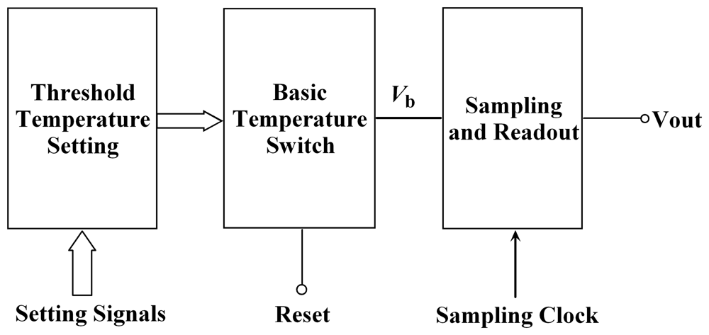
Figure 1 shows a block diagram of the proposed CMOS temperature switch. It consists of a basic temperature switch circuit, a threshold temperature setting module and a sampling and readout module. The operation of the basic temperature switch circuit depends on chip temperature, and changes abruptly when the temperature increases to a critical temperature. The critical temperature is called as the threshold temperature Tth that can be programmed. The basic temperature switch circuit can automatically compensate Tth variation due to process tolerance. The threshold temperature setting module is used to control the value of Tth by an external threshold setting signal. The sampling and readout module samples a switch signal and then outputs a digital signal at a fixed frequency.
2.1. The Basic Temperature Switch Circuit and Threshold Temperature Tth
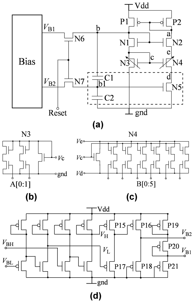
The basic temperature switch circuit is shown in Figure 2 (a). It consists of two PMOS transistors P1 and P2, seven NMOS transistors N1, N2, N3, N4, N5, N6 and N7, two capacitors C1 and C2, and a bias voltage circuit. The P1, P2, N1, N2, N3, N4 and N5 transistors constitute the temperature switch core circuit. It is similar to the β multiplier circuit [3]. But, the linear resistor in the multiplier circuit is substituted by the transistor N5 [2]. N3 and N4 represent two equivalent nMOS transistors whose ratios of width and length can be adjusted by logic signals from the threshold temperature setting module, respectively. Their actual schematics of the equivalent N3 and N4 transistors are shown in Figure 2 (b) and (c). The transistor N5 and two capacitors C1 and C2 constitute equivalently a floating gate MOS circuit and the transistors N6 and N7 are switches that are controlled by periodical signal RESET. The operation is as follows. First the N6 and N7 transistors are switched on, the voltages Vb and Vb1 at the nodes b and b1 are preset to be equal to VB1 and VB2, respectively. Then N6 and N7 are switched off and the circuit transit into a stable state automatically. When the temperature is lower than Tth, in the final stable state, the transistors P1 and P2 operate in saturation region, while transistors N1, N2, N3 and N4 in subthreshold region, transistor N5 in linear region and Vb and Vb1 maintain at about several hundred milivoltage. As long as the temperature increases and exceeds to Tth, the final state of the basic temperature switch circuit changes abruptly: the MOS transistors (P1, P2, N1-N5) cut off, and Vb and Vb1 drop almost to zero. The threshold temperature Tth of the switch can be preset by adjusting the ratios of width and length of N3 and N4 transistors. The bias voltages VB1 and VB2 are supplied by the bias voltage circuit, shown in Fig. 2(d). VB1 is not dependent on the process tolerance and the chip temperature; VB2 depends on the threshold voltage variation of the MOS transistor and has a very small temperature coefficient. The bias voltage circuit is used for resetting the temperature switch circuit periodically and compensating for Tth variation due to process tolerance
The basic relationship among Vb, Vb1 and T is presented in[4]. Considering the body-effect and temperature effect, the relationship among Vb, Vb1 and T can be rewritten as
where
,
,
,
, γ is the body-effect coefficient, VTH0 is the zero-bias threshold voltage at absolute zero temperature, KT is the zero-bias threshold voltage temperature coefficient (to simplify the analysis, KT here equals −KT1/TNORM in [5]), T is the temperature, K is Boltzmann constant, ξ is the subthreshold swing parameter, W and L are the channel width and length respectively, Kij = (W/L)i /(W/L)j and the footnote numbers represent transistor numbers.
If the floating gate MOS circuit is not used(taking out the capacitors C1 and C2) and Vb is connected with Vb1 directly(just as [2,6]), differentiating both sides of Eq. (1) with T, the derivative of voltage Vb w.r.t temperature is given by
The denominator in Eq. (2) decreases with temperature. At the threshold temperature Tth, the denominator becomes to be 0 and the differentiation of the voltage Vb becomes negative infinity. This indicates that at the threshold temperature Tth the circuit performs a switching operation. Assuming that the denominator in Eq. (2) equals 0, we can get
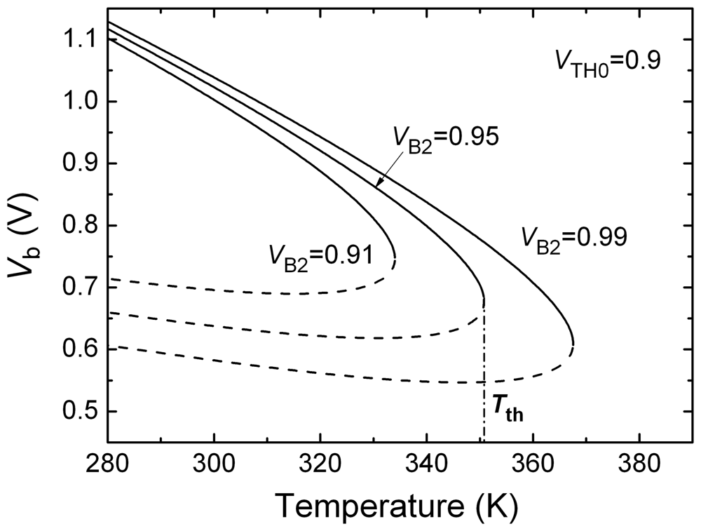
In Eq. (4) the derivative of Tth w.r.t VTH0 is larger than zero, so Tth increases linearly with VTH0 and the slope is very sharp. Figure 3 shows the calculated dependence of Vb on temperature T with three different threshold voltages. It indicates that the threshold temperature Tth depends strongly on the threshold voltage of MOS transistor. A VTH0 variation of 50mV results in a Tth change of 20 K. In these calculations we used the following conditions: ξ=1.65, K43=2, γ=0.7 V1/2, KT =1.1mv/K. The curves show that there are two solutions for a certain temperature only if the temperature is lower than a critical temperature. The solution with a larger Vb corresponds to the stable operating state of the switch circuit. The transistor N1, N2, N3 and N4 operate in the subthreshold region. The solution with a small smaller Vb is a pure mathematic one and does not correspond to the physical state of the switch circuit. It is not taken into account in the study. When the temperature increases to and exceeds the critical temperature, the operation of the circuit changes suddenly and all of the transistors N1, N2, N3, N4, N5, P1 and P2 cut off so that no solution can be obtained by the above equations and Vb becomes almost zero. The critical temperature is considered as the threshold temperature Tth. The N1, N2, N3 and N4 transistors in the switch are all in the subthreshold region, so the currents through them are quite small and power consumption is very low.
2.2. Compensation for Tth Variation
Equation (4) and Figure 3 show the strong dependence of Tth on VTH0. This indicates that the variation of VTH0 results in a large warp of Vb (or Vb1), and then makes Tth change so that the temperature switch does not operate well. If the warp of Vb1 could be compensated, Tth may keep independent on variation of VTH0. We design a floating gate neural MOS circuit[7] to compensate Tth variation. The circuit is surrounded by a dashed line box in Figure 2 (a). If the switches N6 and N7 are on, biases VB1 and VB2 preset the voltages at nodes b and b1, respectively. If the ratio of C1 and C2 is M, Vb1 equals VB2 −(VB1 − Vb) . M/(M + 1). Substitute it into Eq. (1) and repeat the derivation as the above, we can get:
It is found that Vb and Tth both increase with VB2 when other parameters keep invariable. Figure 4 shows the dependence of Tth on VB2 with VB1=1.1V. If we design a bias circuit to make VB1 remain almost invariable with VTH0 and VB2 vary suitably with VTH0, the Tth variation could be compensated by presetting the voltages of node b and b1 with VB1 and VB2. Figure 2(d) shows the schematic of the VB1 and VB2 bias circuit that provides biases VB1 and VB2 for the floating gate neural MOS circuit. If we optimize the sizes of transistors reasonably, VH and VL can vary linearly with VTH0 and their temperature coefficients are almost same. P15, P16, P17 and P18 constitutes a subtracter [8] and make VB2 equal VH − VL. VB2 varies linearly with VTH0 and its temperature coefficient is small. On the other hand, VB1 almost does not change with VTH0 and temperature. It can be obtained by using transistors P19, P20 and P21 to divide the power supply voltage.
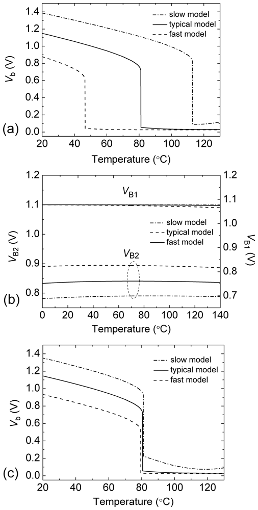
We simulated the performance of the temperature switch circuit with three transistor models corresponding to three process corners: slow model, typical model and fast model. It is considered that the effect of VTH0 variation on Tth is dominant when the transistor model is changed. Figure 5 (a) shows the Tth variation that is originated by different process corners without compensation. The Tth variation is larger than 60°C. Figure 5 (b) shows the dependences of VB1 and VB2 on the temperature and the process corner. VB1 does not change almost with the process corner and the temperature. On the other hand, VB2 varies linearly with the process corner and its temperature coefficient is small. Figure 5(c) shows the switch characteristics of the temperature switch circuit with the compensation operation in three process corners. We can see that the compensation for the process corner or VTH0 variation is very effective.
2.3. Control of hysteresis
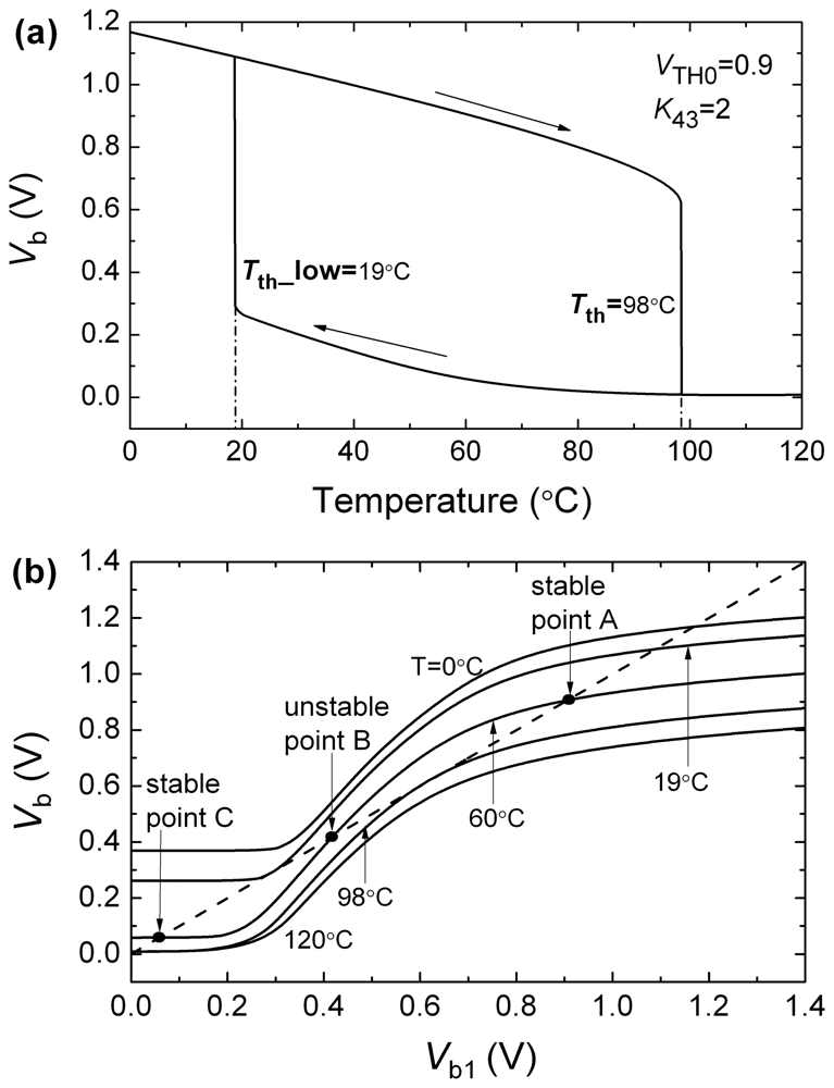
We use HSPICE to simulate the operation of the temperature switch circuit. Figure 6(a) gives the dependence of Vb on the chip temperature. The T dependence of Vb shows the hysteresis behavior reported also by [6]. First Vb decreases with the increase of the temperature. When the temperature increases to Tth = 98°C, Vb abruptly drops down to a lower voltage. Then, when the temperature is decreased from the high temperature and becomes lower than Tth, Vb does not rebound to a higher voltage until the temperature decreases to a temperature point of 19°C which is much lower than Tth.
This hysteresis phenomenon can be analyzed as follows. Assuming that the nodes b and b1 are opened and that a voltage Vb1 is biased at node b1, the voltage Vb will change with Vb1. Figure 6(b) shows the dependence of Vb on Vb1 at different temperatures and Vb1 straight line. If the b and b1 nodes are connected and Vb is equal to Vb1 in the temperature switch circuit, the intersections of Vb curves and Vb1 straight line can be considered as the operating points of the switch circuit. At the temperature of 60°C, the Vb curve intersects Vb1 line at three points of A, B and C. The A and C points correspond to the stable operating points, and B is an unstable point. If the initial Vb is higher than the voltage of the point B, the circuit will settle down to the stable point A. In contrast, if the initial Vb is lower than the voltage of the point B, it will settle down to point C. Therefore, if the initial Vb is higher than the voltage of the point B and the temperature is increased gradually, the switch circuit changes its operating state along a series of A points. When the temperature increase to and exceeds Tth of 98°C, the Vb curve intersects Vb1 line only at the C point so that the switch circuit shifts suddenly its state from A to C point and shows a switching operation. If the temperature decreases from a temperature higher than Tth, the circuit operates at the point C because Vb is smaller than the point B. When the temperature decreases to and is under a critical point of 19°C, the C point disappears and the switch circuit shifts suddenly its operating state from C to A point. Thus, the switch circuit shows the hysteresis behavior which is too large to perform the temperature switch operation well.
How to control the hysteresis is a study issue. We propose a simple method to remove the hysteresis equivalently or to change hysteresis. A bias and resetting circuit is designed in the basic temperature switch circuit, as shown in Figure 2(a). The bias and resetting circuit consists of a VB1 and VB2 bias voltage circuit, the N6 and N7 resetting-switch transistors and a resetting signal RESET. If the RESET signal is periodic and synchronizes with the operation of sampling and readout module, Vb will be preset periodically to make the circuit operate at the A operating point initially and the switch operation of the circuit can be measured correctly without a hysteresis. Furthermore, a suitable hysteresis is often required in a practical application. We can integrate two switch circuits with different Tth1 and Tth2 (Tth1 < Tth2) and realize a temperature switch with a hysteresis of ΔT = Tth2 - Tth1. The sampling and readout module measures the Vb voltages of the two switch circuits and outputs a switch signal and a rebound signal when T ≥Tth2 and T < Tth1, respectively.
2.4. Programmable Tth
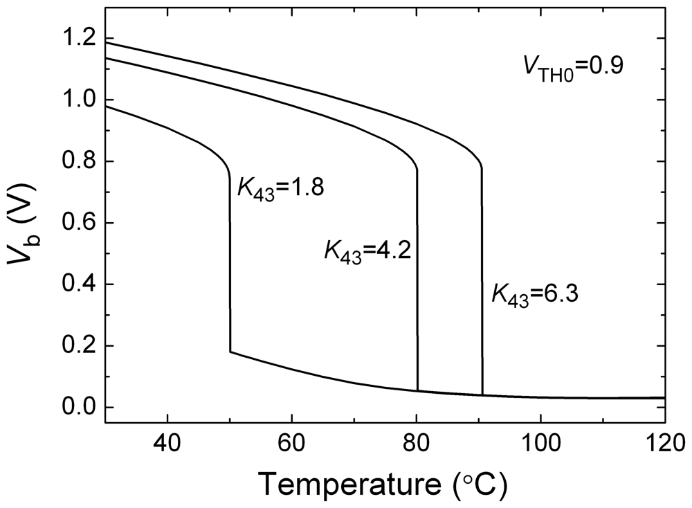
In practice it is always expected that the threshold temperature Tth of the proposed temperature switch can be programmed. Equation (4) indicates that Tth increases nonlinearly with the increase of ratio K43 of ratios of width and length of N3 and N4 transistors. The transistors N3 and N4 are two equivalent nMOS transistors whose efficient ratios of width and length can be adjusted by some parallel transistors and logic-controlled switches, as shown in Figure 2(b) and 2(c). The logic-control signals are supplied by the threshold temperature setting module. Thus we can program value of Tth by tuning up the ratios of width and length of N3 and N4, respectively. Because the change of Tth depends nonlinearly on K43, additional compensating circuits are required, such as the rightmost 4 branches in Figure 2 (c). Figure 7 shows the dependence of Vb on temperature with different K43 parameters. The results indicate that the threshold temperature Tth of the temperature switch can be programmed by controlling the ratio K43.
2.5. Influence of Mismatch and Vdd variation on Tth
From Eq. (5), we can see that K43, M, VB1 and VB2 are the main parameters that determine the value Tth, while the influence of size variations of other transistors is not evident. First the K43 is the ratio of the sizes of N4 and N3 transistors. N4 and N3 are, respectively, composed of several transistors which are integer multiples of the basic unit transistor. When the circuit layout are designed, we can make N3 and N4 transistors match well so that the process variation of K43 is smaller than 1%. Then M is the ratio of the capacitor C1 to the capacitor C2. In the modern CMOS process, the process variation of the ratio M can be controlled to be below 1% by the capacitor matching technique. Therefore the process variation of M almost does not influence the value Tth. Finally when a Vdd variation happens, VB1 and VB2 change in the same orientation linearly. If Vdd varies within ±10%, the change of (M + 1)VB2 − MVB1 can be limited in ±1.5mV with an appropriate value of M. From Eq. (5), the variations of K43, M and Vdd make Tth vary within ±1°C.
3. Implementation of Temperature Switch
The temperature switch circuit was implemented in a standard 0.35μm CMOS process. The basic temperature switch circuit, the threshold temperature setting module and the sampling and readout module were integrated. The basic temperature switch is analog circuit. The threshold temperature setting module and the sampling and readout module are logic circuits. In order to make the compensation for the Tth variation effective, the VB1 and VB2 bias circuit was placed near the devices in the temperature switch core circuit. Sixteen different Tths can be set from +45°C to +120°C in a 5°C increment. Simulated results indicates that the setting error of the threshold temperature Tth is kept within ±2°C in a normal variation range of the process.
4. Measurement Result
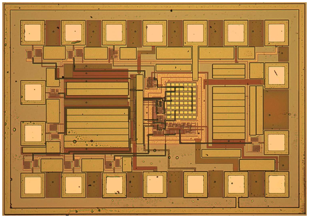
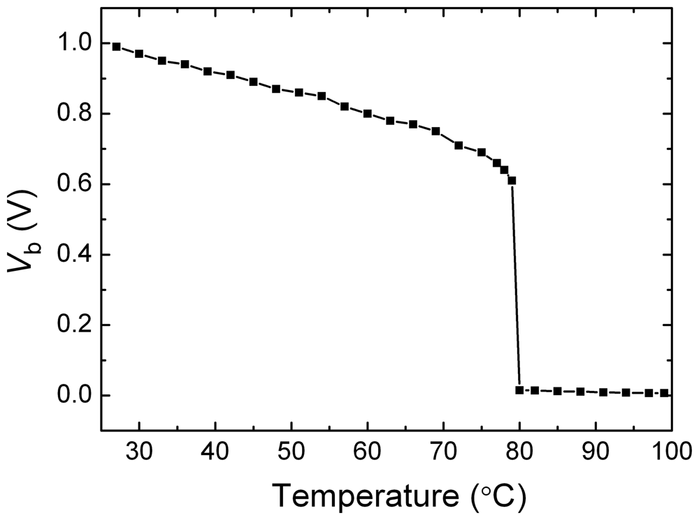
The chip microphotograph is shown in figure 8. The chip core area is only 0.04 mm2. After its Tth was set, we changed the temperature and measured the voltage Vb at a sampling frequency of 2Hz. Figure 9 gives the measured typical dependence of Vb on temperature T. It shows a very good temperature switch characteristic with the threshold temperature Tth of 80°C. At the threshold temperature, the sampling and readout module also outputs a switching signal. We programmed the threshold temperature Tth with external digital codes, and a series of the measured Tth values could be obtained. Figure 10 shows the measured error in the threshold temperatures for 3 samples. The design parameters and the measured results are presented in table 1. In order to compare the switch with other CMOS temperature switch and temperature sensor reported [1,9], the parameters and the measured results of the CMOS temperature switch and temperature sensor are also listed in table 1. Note that the circuit in [9] is a temperature sensor whereas the presented circuit and the circuit in [1] are temperature switch.
5. Conclusion
A novel uncalibrated(need not to be uncalibrated after fabrication) CMOS programmable temperature switch has been presented with extremely low power consumption, high temperature setting accuracy and small chip area. The threshold temperature Tth could be programmed by changing the efficient ratio of width and length of the MOS transistors. The threshold temperature variation due to process tolerance has been compensated automatically by a floating gate neural MOS circuit and a bias circuit with resetting switches. The circuit has been implemented in a standard 0.35μm CMOS process. Sixteen different Tths can be set from +45°C to +120°C in 5°C increments. The measurement shows a good consistency in the threshold temperatures for 3 samples. The chip core area is 0.04 mm2. Its power consumption is only 3.1μA at 3.3V supply. The temperature switch has the advantages: low power consumption, the programmable threshold temperature, automatic compensation for process tolerance and the controllable hysteresis.
Acknowledgments
The authors would like to thank Qingyu Lin, Wancheng Zhang and Zhiqing Geng for useful discussions and simulation, Xiaozhou Yan for layout design, Wei Miao for design of control logic and test work.
References and Notes
- Schinkel, D.; de Boer, R.P.; Annema, A.J.; van Tuijl, A.J. A 1-V 15uW High-Precision Temperature Switch. Proceedings of the 27th European Solid-State Circuits Conference, Villach, Austria, September 2001; pp. 104–107.
- Hagiwara, A.; Hirose, T.; Yamada, H.; Asai, T.; Amemiya, Y. Critical temperature switch consisting of CMOS circuits. Proceedings of the Society Conference of IEICE, Sapporo, Japan, September 2005; p. 101.
- Baker, R.J.; Li, H.W.; Boyce, D.E. CMOS Circuit Design, Layout, and Simulation; Wiley-IEEE Press: New York, NY, USA, 1997; pp. 480–481. [Google Scholar]
- Li, Y.; Wu, N. A novel programmable CMOS temperature switch. Proceedings of 8th International Conference on Solid-State and Integrated Circuit Technology, Shanghai, China, October 2006; pp. 676–678.
- Liu, W.; Jin, X.; Chen, J.; Jeng, M.C.; Liu, Z.; Cheng, Y.; Chen, K.; Chan, M.; Hui, K.; Huang, J.; et al. BSIM3v3.2.2 MOSFET Model-Users' Manual; Department of Electrical Engineering and Computer Sciences, University of California: Berkeley, CA, USA, 1999. [Google Scholar]
- Hagiwara, A.; Hirose, T.; Yamada, H.; Asai, T.; Amemiya, Y. Critical temperature switch consisting of Subthreshold CMOS circuits. IEICE Trans. Electron 2006, J89-C, 654–656. [Google Scholar]
- Shibata, T.; Ohmi, T. Neuron MOS Binary-Logic Integrated Circuits-Part I: Design Fundamentals and Soft-Hardware-Logic Circuit Implementation. IEEE Trans. Electron Devices 1993, 40, 570–576. [Google Scholar]
- Sengupta, S. An Input-Free Nmos Vt Extractor Circuit In Presence Of Body Effects. Proceedings of IEEE International Symposium on Circuits and Systems, Vancouver, BC, Canada, May 2004; pp. I-912–I-915.
- Bakker, A.; Huijsing, J.H. Micropower CMOS Temperature Sensor with Digital output. IEEE J. Solid-State Circuit 1996, 31, 933–937. [Google Scholar]
Figure 1.
Block diagram of the proposed temperature switch.

Figure 2.
(a) The schematic of the basic temperature switch; (b) the actual schematic of the equivalent N3 transistor; (c) the actual schematic of the equivalent N4 transistor; (d) the schematic of the VB1 and VB2 bias circuit that provides biases VB1 and VB2 for the floating gate neural MOS circuit.

Figure 3.
The dependence of Vb on temperature T with three different threshold voltages. It's calculated based on Eq. (6). ξ=1.65, γ=0.7V1/2, KT=1.1mV/K, K43=2, K31=1.4 and K35=560.
Figure 3.
The dependence of Vb on temperature T with three different threshold voltages. It's calculated based on Eq. (6). ξ=1.65, γ=0.7V1/2, KT=1.1mV/K, K43=2, K31=1.4 and K35=560.

Figure 4.
The dependence of Tth on VB2 It's calculated based on Eq. (6) and Vb1 = VB2 −(VB1 − Vb) . M/(M + 1) .ξ=1.65, γ=0.7V1/2, KT =1.1mV/K, K43=2, K31=1.4, K35=560 and M=38/11.
Figure 4.
The dependence of Tth on VB2 It's calculated based on Eq. (6) and Vb1 = VB2 −(VB1 − Vb) . M/(M + 1) .ξ=1.65, γ=0.7V1/2, KT =1.1mV/K, K43=2, K31=1.4, K35=560 and M=38/11.

Figure 5.
(a) The simulated dependence of Vb on temperature T with three different models before compensation. VB1=1.1V and VB2=0.84V. (b) The simulated dependence of VB1 and VB2 on temperature T with three different models. (c) The simulated dependence of Vb on temperature T with three different models after compensation. VB1 and VB2 are supplied by the bias circuit.

Figure 6.
(a) Dependence of Vb on the chip temperature. The temperature switch shows hysteretic characteristic. It's the simulation result of the temperature switch core circuit with the node b and b1 connecting directly; (b) the dependence of Vb on Vb1 at different temperatures and Vb1 straight line. The Vb curve intersects Vb1 line at three points of A, B and C.

Figure 7.
Voltage Vb as a function of temperature with different K43 parameters.

Figure 8.
Chip microphotograph of the temperature switch.

Figure 9.
The measured dependence of Vb on temperature T.

Figure 10.
The measured error in the threshold temperatures for 3 samples.


Table 1.
Measured characteristics of the temperature switch and comparison with the temperature switch and sensor reported.
| This work | [Schinkel] | [Bakker*] | |
|---|---|---|---|
| Supply voltage | 2.3—3.3 V | 1.0—1.8V | 2.2—5V |
| Supply current T=25°C | 3.1μA | 13μA | 25μA |
| Core area | 0.04 mm2 | 0.03 mm2 | 1.5 mm2 |
| Switch temperature | 45—120°C with 5°C increase | 128.5°C | – |
| Inaccuracy(3σ) | <2°C(typical error) | 1.1°C | 1°C |
| Calibration | No | No | Yes |
| DC supply sensitivity | 1°C/V (2.7V—3.3V) | 0.05°C/V | 0.1°C/V |
| Hysteresis | 0°C | 1.2°C | – |
*Most of the research of temperature sensor in recent years are focused on high accuracy and they have much higher consumptions. They are not suitable to compared with our design, so we select this earlier paper for a comparison. The circuit was a state-of-the-art, calibrated and chopped, CMOS temperature sensor.
© 2008 by the authors; licensee Molecular Diversity Preservation International, Basel, Switzerland. This article is an open-access article distributed under the terms and conditions of the CreativeCommons Attribution license ( http://creativecommons.org/licenses/by/3.0/).
Share and Cite
MDPI and ACS Style
Li, Y.; Wu, N. A Low-Cost CMOS Programmable Temperature Switch. Sensors 2008, 8, 3150-3164. https://doi.org/10.3390/s8053150
AMA Style
Li Y, Wu N. A Low-Cost CMOS Programmable Temperature Switch. Sensors. 2008; 8(5):3150-3164. https://doi.org/10.3390/s8053150
Chicago/Turabian StyleLi, Yunlong, and Nanjian Wu. 2008. "A Low-Cost CMOS Programmable Temperature Switch" Sensors 8, no. 5: 3150-3164. https://doi.org/10.3390/s8053150