1. Introduction
With the advances in science and technology, industrial communication has become inseparable from daily life. According to a report from the National Communications Commission in Taiwan, the penetration rate of the mobile phone in Taiwan was only 6.9% in 1997, and grew to 105.8% in 2007. As the size of these devices continues to decrease, a filter is needed to control the quality of communication. Filters have become an important electronic component within the electronic industry in order to keep pace with the developments that are being made rapidly. Micromechanical resonators can be used as filters for wireless communication applications [
1,
2]. The main advantage of micromechanical resonators is high quality factor (Q-factor).
Many studies have recently used microelectromechanical systems (MEMS) technology to fabricate micromechanical resonators. For example, Yao
et al. [
3] proposed a single-crystal silicon (SCS) micro tunable resonator fabricated by reactive ion etch (RIE) process and microfabrication technique, which the tunable resonator had a driving voltage of 35 V, a Q-factor of 10,000 in vacuum and a tuning range of 60 kHz. Patil
et al. [
4] fabricated a thin film silicon microbridge resonator on a glass substrate using surface micromachining. The structural material of the resonator was a bilayer of aluminum and phosphorus-doped hydrogenated amorphous silicon, and the sacrificial material was polynorbornene. The resonant frequency and Q-factor of the microbridge resonator were about 4.4 MHz and 450, respectively. Zhang
et al. [
5] utilized surface micromachining to manufacture a bridge microresonator with a conductive polymer blend as the structural layer, and the sacrificial layer was aluminum. The resonant frequency of the resonator was about 3 MHz, and the Q-factor was 100 in vacuum. The polycrystalline 3C silicon carbide (polySiC) lateral resonators, proposed by Roy
et al. [
6], were made by a three-mask surface micromachining process using silicon dioxide, polysilicon, and nickel as the isolation, sacrificial, and contact metallization layers, respectively. The driving voltage and Q-factor of the ploySiC resonators at atmospheric pressure were 40–170 V and 148, respectively. The polySiC resonators had a driving voltage of about 1 V and a Q-factor of over 100000 under high vacuum condition (< 10-5 torr). Dai
et al. [
7] presented a tunable resonator fabricated by using the CMOS-MEMS process. This resonator could be tuned when applying a dc bias to a comb of linearly varied finger length; the driving voltage was approximately 20 V. Using the same process, Dai
et al. [
8] manufactured a plane resonator, and the driving voltage and the resonant frequency were 60 V and 39.5 MHz, respectively.
The CMOS-MEMS technique [
9–
11] is the use of a commercial CMOS process to fabricate MEMS devices. Micro devices manufactured by the CMOS-MEMS technique usually need some post-processing to release the suspended structures or coat the functional films. For instance, the suspended structures of the CMOS-MEMS pressure sensors [
12] were released by a wet etching post-process, and the film sensitive to ammonia [
13] was coated by a post-process. In this work, we utilized the CMOS-MEMS technique to make the tunable in-plane resonator. The commercial 0.35 μm CMOS process of the Taiwan Semiconductor Manufacturing Company (TSMC) was used to fabricate the micromechanical resonator. The post-process employed a wet etching treatment to remove the sacrificial layer and release the suspended structures in the resonator. The tunable resonator contains three parts: the driving, sensing, and tuning parts. The sensing part senses a change in capacitance when a voltage is applied to the driving part, and the resonant frequency of the resonator can be tuned by the tuning part. Experimental results depict that the resonant frequency was about 183 kHz, and increased by 14 kHz when a tuning voltage of 30 V was applied.
2. Design and Simulation
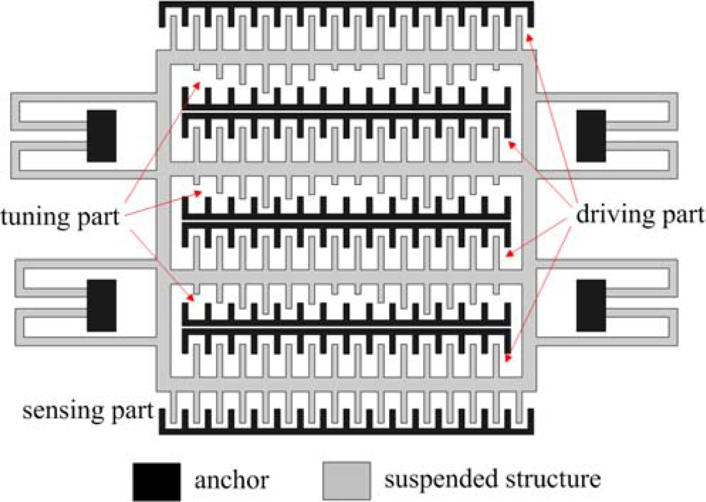
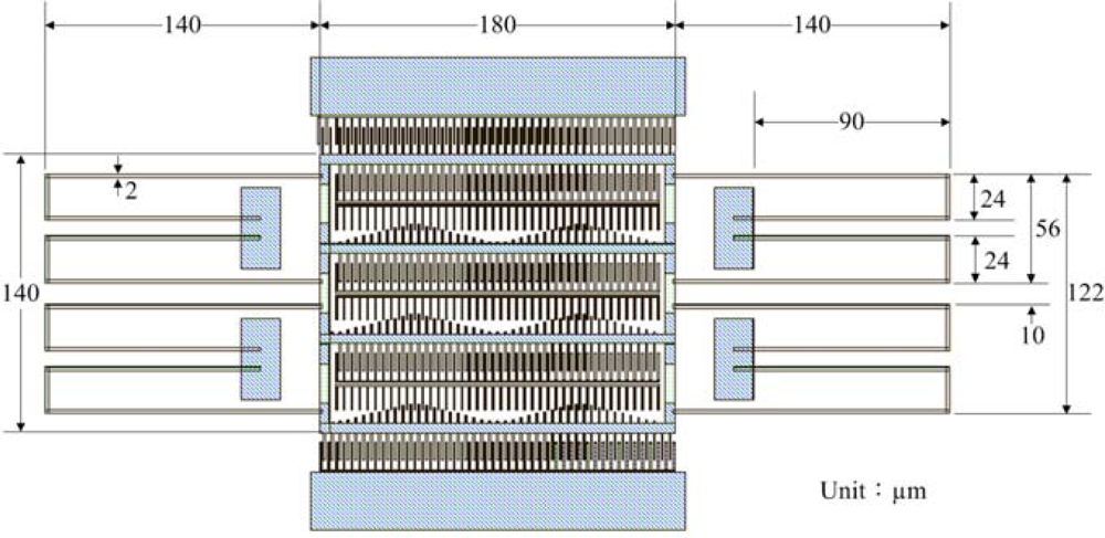
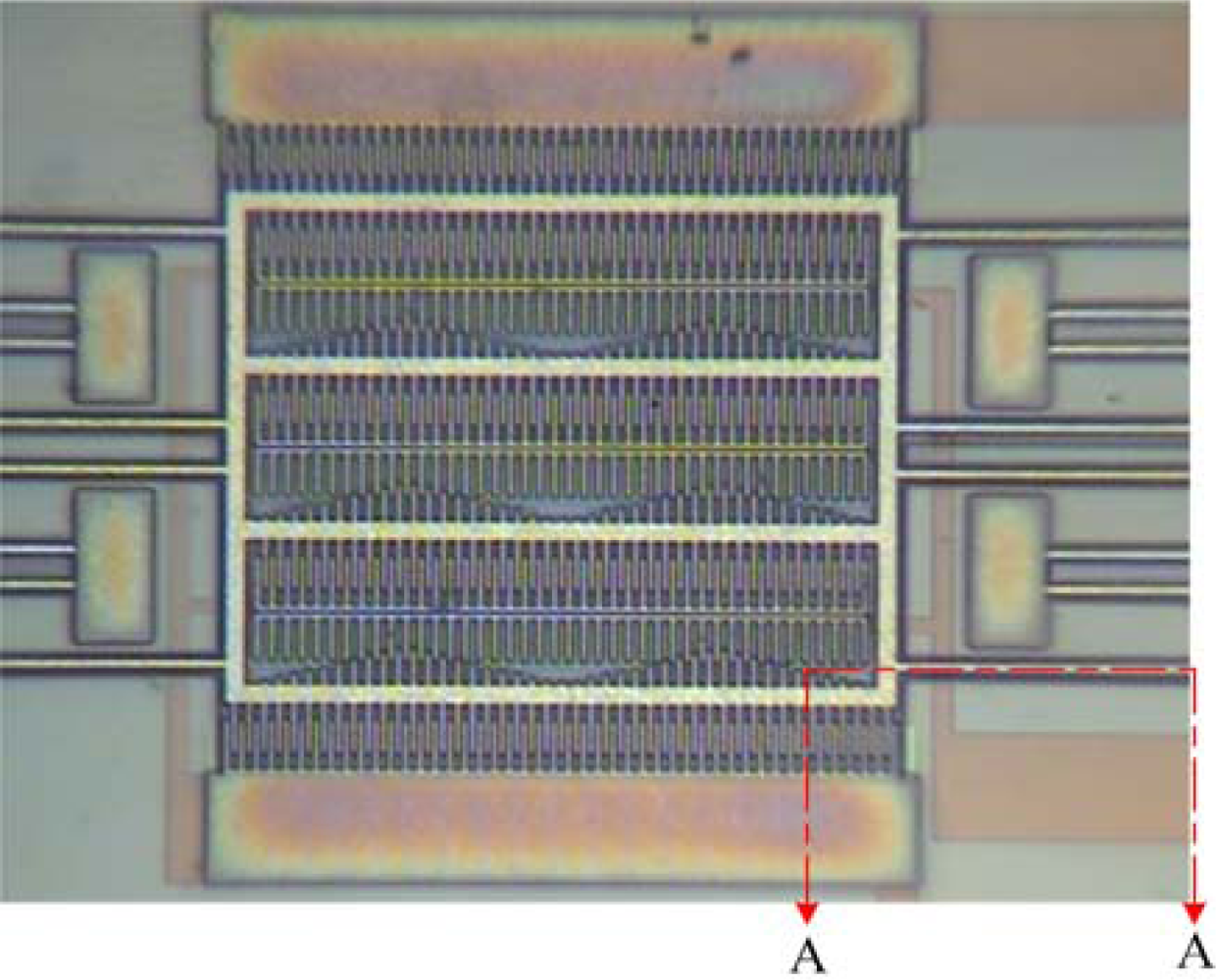
Figure 1 illustrates the structures of the micromechanical resonator, which includes a driving part, a sensing part and a turning part. The sensing and driving parts have a constant-length comb configuration that consists of the moveable and fixed combs. The driving voltage depends on the number of comb-finger of driving part and the stiffness of supported beams. In order to reduce the driving voltage, the driving part of the resonator is designed with four comb-finger rows. There are eight support beams arranged symmetrically. Each beam is 260 μm long, 2 μm wide and 2.6 μm thick, and it is fixed to the 20×40 μm
2 anchor. The resonator is a suspended membrane with a thickness of 5.8 μm; the gap between the membrane and the substrate is approximately 1.3 μm. The area of the resonator is about 460×260 μm
2.
The resonator is actuated by the electrostatic force. When applying an ac voltage,
Vs(
t)=
V0 sin
ωt, to the driving part, the driving force produced by the comb-fingers of the driving part can be expressed as [
14],
and
where
n represents the number of fingers in the driving-comb;
ε is the permittivity constant of air,
th is the comb thickness and
d is the inter-finger gap of the comb. The equation of motion of the micromechanical tunable resonator is given by,
where
m represents the mass of the resonator;
c is the damp;
k is the stiffness of the resonator and
x is the dynamic displacement of the resonator. The particular solution of
Equation (3) can be expressed as [
15],
and
where
X and
ϕ are the amplitude and phase angle of the response, respectively;
r is the frequency ratio and
r=
ω/
ωn;
ζ is the damping ratio and
ζ=
c/
2mωn;
ωn is the natural frequency of the resonator. The maximum amplitude occurs when
[
15]. Substituting
Equation (2) and
into
Equation (5), the maximum amplitude of the micromechanical tunable resonator can be obtained,
In the design, the stiffness of the resonator,
k, is about 17 N/m, and the number of fingers in the driving-comb,
n, is 264. The inter-finger gap of the comb,
d, is 1 μm and the comb thickness,
th, is 5.8 μm.
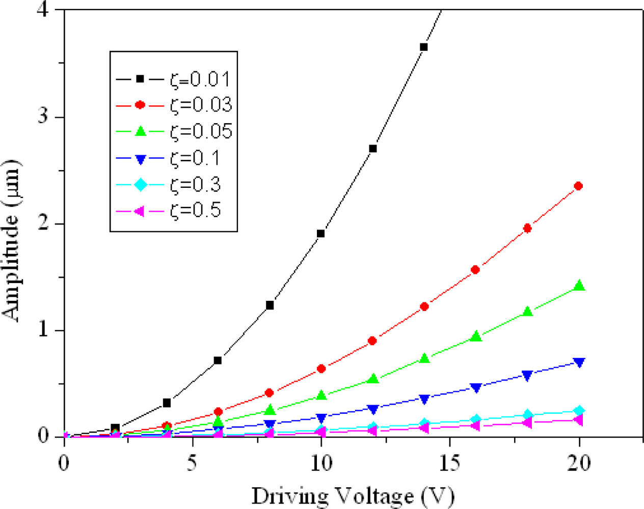
Figure 2 shows the maximum amplitude of the micromechanical tunable resonator with different damping ratios, which is evaluated by
Equation (6). In addition to the geometric shape of the resonator, the maximum amplitude of the resonator depends on the driving voltage and the damping ratio.
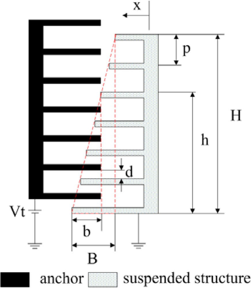
Figure 3 illustrates the geometry of the tuning part in the resonator, which contains the moveable and fixed combs. The moveable comb of the turning part is designed as linearly varied finger length. The resonant frequency of the micromechanical tunable resonator is given by [
7],
and
where
keff represents the effective stiffness of the resonator;
N is the number of fingers in the tuning-comb;
ε is the permittivity constant of air;
H and
B are the width and height of the tuning-comb triangle, respectively;
th is the comb thickness;
Vt is the tuning voltage of the tuning part;
p is the pitch of the tuning-comb fingers;
d is inter-finger gap of the comb;
x is the displacement of the moveable structure; and
b is the overlapping length of the comb finger, as shown
Figure 3. In accordance with
Equation (7), we know that the resonant frequency of the resonator changes as the effective stiffness of the resonator varies. According to
Equation (8), the effective stiffness of the resonator depends on the geometric shape, tuning-comb number, and tuning voltage of the tuning part. Therefore, the resonant frequency of the resonator can be controlled by the tuning part. The effective stiffness increases when applying a tuning voltage to the resonator, so that the resonant frequency of the resonator is increased.
In order to characterize the relation between the effective stiffness, geometric shape, tuning voltage of the tunable resonator,
Equation 8 is arranged as,
and
where
keff/
k denotes the stiffness ratio that is the ratio of the effective stiffness and the stiffness in the resonator;
β is the shape factor related to the geometric shape of the tuning part and the beams and the unit is N
2/V
2·m
2;
Vt/
k is the tuning voltage to stiffness (TVS) ratio that represents the ratio of the tuning voltage and the stiffness in the resonator and the unit is V·m/N. According to
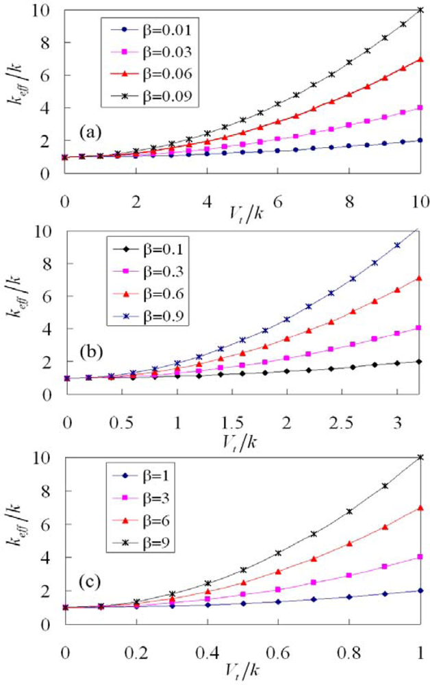
Equation (9), the stiffness ratio of the resonator with different shape factors is plotted in
Figure 4.
The stiffness ratio,
keff/
k, is unity when the tuning voltage is zero; this means that the effective stiffness of the resonator is equal to its stiffness when without tuning driving. As shown in
Figure 4(a), the value of shape factor,
β, is changed from 0.01 to 0.09. The stiffness ratio increases as the shape factor increases under the same tuning voltage. In addition to the shape factor, the stiffness ratio increases as the TVS ratio increases. As shown in
Figure 4(b), the value of shape factor is varied from 0.1 to 0.9. The results show that the stiffness ratio increases as the shape factor and the TVS increase. Under the same stiffness ratio, the TVS ratio (
Vt/
k) in
Figure 4(b) is smaller than that in
Figure 4(a) because the shape factors in
Figure 4(b) have a larger value. For instance, suppose that the resonator requires achieving the stiffness ratio of 10, the TVS ratios are 10 (
Figure 4(a)) and 3.1 (
Figure 4(b)) when the shape factors adopt 0.09 and 0.9, respectively. This means that the TVS ratio can be reduced by using the increment of shape factor. As shown in
Figure 4(c), the value of shape factor is changed from 1 to 9. The trends of curves in
Figure 4(c) are similar to that in
Figure 4(a) and
4(b). The results show that the TVS ratio corresponding to the stiffness ratio of 10 at the shape factor of 9 is unity.
The resonant frequency of the tunable resonator depends on its stiffness ratio.
Equation (7) can be written as,
where 2
πf/
ωn is the frequency ratio that is the ratio of the resonant frequency and the natural frequency (
) in the resonator; and
keff/
k is the stiffness ratio of the resonator. According to
Equation (11), we know that the frequency ratio is proportional to the square of the stiffness ratio.
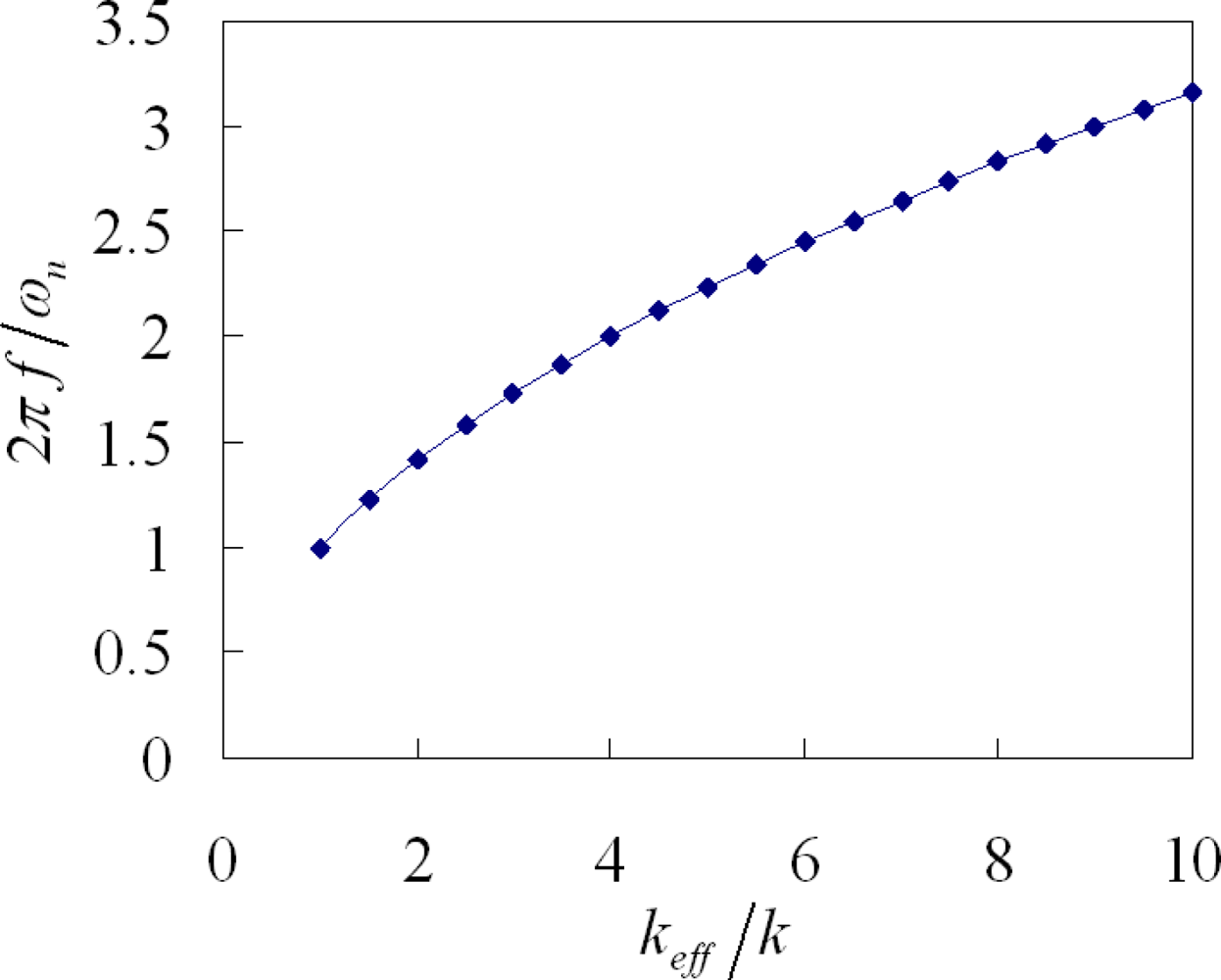
Figure 5 shows the frequency ratio of the tunable resonator, which is computed by
Equation (11). The results depict that the frequency ratios of the resonator are 1 and 3.16 corresponding to the stiffness ratios of 1 and 10, respectively.
The frequency ratio of the resonator relies on its tuning voltage to stiffness ratio. Substituting
Equation (9) into
Equation (11), the frequency ratio of the tunable resonator can be expressed as,
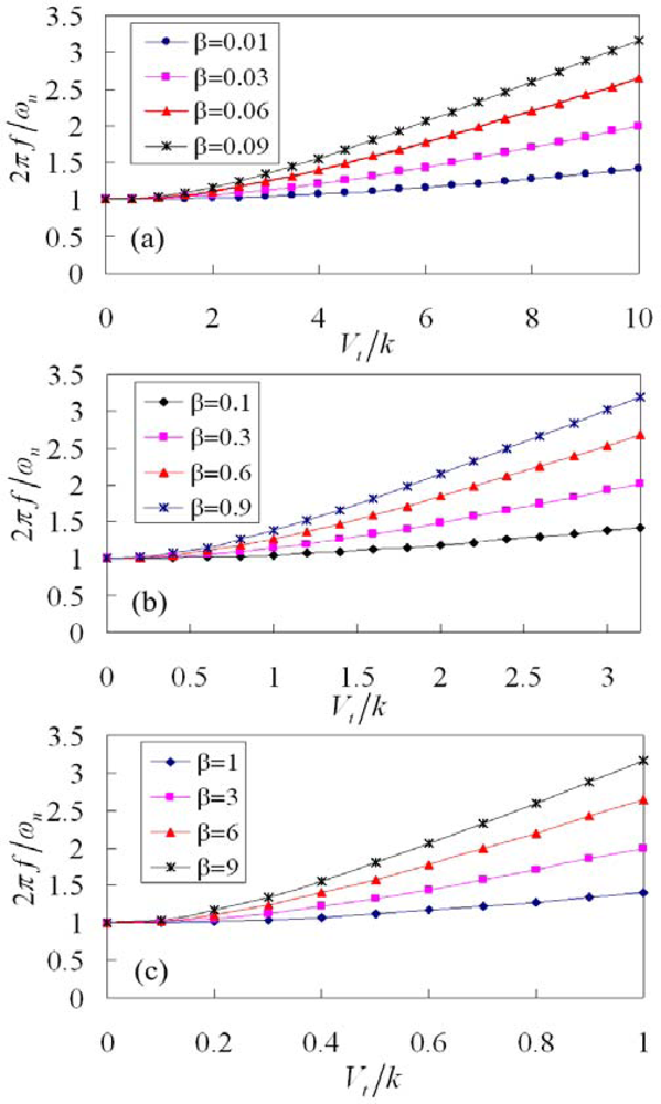
Figure 6 illustrates the frequency ratio of the tunable resonator with different shape factors, which is evaluated by
Equation (12). The values of shape factor in
Figure 6(a), (b) and (c) are 0.01–0.09, 0.1–0.9 and 1–9, respectively. The frequency ratio of the resonator is unity when the tuning voltage,
Vt, is zero; this means that the resonant frequency of the resonator is equal to its natural frequency when without tuning driving. The trends of curves in
Figure 6(b) and (c) are similar to that in
Figure 6(a). The scales of y-axis (frequency ratio) in
Figures 6(a)–(c) are the same, and the scales of x-axis (
Vt/
k) are different. Under the same frequency ratio, the TVS ratio in
Figure 6(b) is smaller than that in
Figure 6(a) due to the shape factors in
Figure 6(b) have a larger value. For example, suppose that the resonator requires achieving the frequency ratio of 1.4, the TVS ratios are 10 (
Figure 6(a)), 3.1 (
Figure 6(b)) and 1 (
Figure 6(c)) when the shape factors adopt 0.01, 0.1 and 1, respectively. Therefore, the frequency ratio increases as the TVS ratio increases. In addition to the TVS ratio, the frequency ratio increases as the shape factor increases at the same tuning voltage.
The resonant frequency of the tunable resonator by
Equation (12) can be written as,
By
Equations (12) and
(13), we know that the resonant frequency of the resonator can be obtained if the frequency ratio, 2
πf/
ωn, is given. The resonant frequency of the resonator relies on the natural frequency, the shape factor and the TVS ratio. The shape factor (
Equation 10) is proportional to the parameters of
N,
H,
ε,
b,
th and
k, and is inverse proportional to the parameters of
B,
p and
d. If the design of the tunable resonator needs a large shape factor, then the parameters of
N,
H,
ε,
b,
th and
k should be increased and the parameters of
B,
p and
d should be reduced. As shown in
Figure 6, the shape factor should consider adopting a larger value if wishing to obtain a low TVS ratio. The procedure of design includes: (1) the specification of the resonator must be determined before the design of the resonator; (2) the frequency ratio of the resonator is obtained according to its specification; (3) the TVS ratio and the shape factor of the resonator can be found in accordance with its frequency ratio and the results in
Figure 6; (4) the geometric shape and stiffness of the resonator are evaluated by means of the shape factor (
Equation 10).
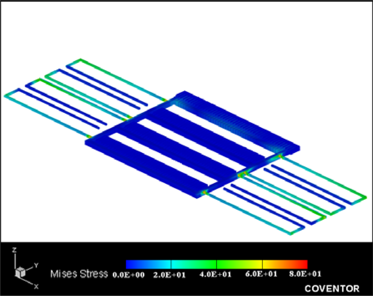
The finite element method (FEM) software, Coventor Ware, is employed to simulate the stress distribution of the micromechanical resonator.
Figure 7 presents the stress distribution of the simulated resonator under a driving voltage of 30 V. The maximum stress of the resonator is 80 MPa, which is located at the fixed end of the beams. The structure is an elastic deformation if the maximum stress is below the yield strength of its material. The resonator is made of aluminum and tungsten. The yield strength of aluminum and tungsten is about 135 MPa [
16] and 450 MPa [
17], respectively. Since the maximum stress of the resonator is less than the yield strength of aluminum, the resonator can be operated in an elastic range under a driving voltage of 30 V.
4. Results and Discussion
The sensing part of the resonator generated a change in capacitance when applying a driving voltage to the driving part.
Figure 12 illustrates the sensing circuitry of the tunable resonator [
19].
The sensing circuitry was used to convert the capacitance variation of the sensing part in the resonator into the output voltage. The experimental setup for measuring the frequency response of the resonator included a power supply, a function generator, and a spectrum analyzer. The power supply provided a dc bias voltage to the tuning part, and the function generator supplied a swept sine voltage of 10 V to the driving part in the resonator to actuate the moveable comb. The spectrum analyzer was utilized to measure the frequency response of the resonator.
Figure 13 displays the frequency response of the resonator with different tuning voltages. The measured result showed that the resonant frequency of the resonator without the tuning voltage was 183 kHz.
The Q-factor of the resonator is given by,
where
f0 is the resonant frequency, and (Δ
f)
3dB is the -3dB peak width. The Q-factor of the resonator was approximately 400, which was calculated by
Equation (14). When the different tuning voltages were applied to the tuning part, the resonant frequency of the resonator changed. As shown in
Figure 13, the experimental results depicted that the resonant frequency of the resonator was 184, 185, 187, 190, 193 and 197 kHz upon applying the tuning voltage of 5, 10, 15, 20, 25 and 30 V, respectively.
The resonator burned when the tuning voltage was over 30 V. The simulated resonance frequency of the resonator with different tuning voltages is shown in
Figure 14, which is calculated by
Equation (13). The simulation presented that the resonator without the tuning voltage had a resonant frequency of 173 kHz, and its resonant frequency changed to 173, 177, 180, 183, 187 and 193 upon applying the tuning voltage of 5, 10, 15, 20, 25 and 30 V, respectively. The simulated results were in agreement with the measured results. Both of results showed that the resonant frequency of the resonator increased as the tuning voltage increased.
Figure 14 shows the measured and simulated results for the resonant frequency of the tunable resonator at the different tuning voltages, where the measured data are from
Figure 13. The measured results showed that the resonant frequency changed from 183 kHz to 197 kHz when the tuning voltage increased from 0 V to 30 V, an increase of 14 kHz with a tuning voltage of 30 V. Therefore, the maximum frequency-tuning range of the resonator was about 7.6%. As shown in
Figure 14, when the tuning voltage increased from 0 V to 30 V, the simulated results presented that the resonant frequency changed from 173 kHz to 193 kHz, and the measured results showed that the resonant frequency varied from 183 kHz to 197 kHz. The error percentage of both results was below 5.8%, which was small and reasonable, and was the reason that the surface of the structural layers had a little residual oxide resulting in the increment of the stiffness and the resonant frequency.
The tunable resonator reported by Yao
et al. [
3], had a driving voltage of 35 V. The driving voltage of the tunable resonator, manufactured by Dai
et al. [
7], was about 20 V. Dai
et al. [
8] proposed a plane resonator that the driving voltage was about 60 V. Comparing with the above literature, the driving voltage of this work was lower than that of Yao
et al. [
3] and Dai
et al. [
7,
8].


