Article

Electromechanical Characteristic Analysis of Passive Matrix Addressing for Grating Light Modulator

1
The Key Laboratory of Fundamental Science of Micro/Nano Device & System Technology, Chongqing university, Chongqing, 400044, P.R. China
2
Optoelectronic Engineering Department, Chongqing University, Chongqing, 400044, P.R. China
*
Author to whom correspondence should be addressed.
Sensors 2009, 9(3), 2162-2175; https://doi.org/10.3390/s90302162
Submission received: 23 January 2009 / Revised: 5 March 2009 / Accepted: 19 March 2009 / Published: 24 March 2009

Abstract

:
A Grating Light Modulator (GLM) based on Micro-Electro-Mechanical Systems (MEMS) is applied in projection display. The operating principle of the GLM is introduced in this paper. The electromechanical characteristic of the passive matrix addressing GLM is studied. It was found that if the spring constant is larger, both the response frequency and the driving voltage are larger. Theoretical analysis shows that the operating voltage and the pull-in voltage of the GLM are 8.16 and 8.74 V, respectively. When an all-selected pixel in a m×n array is actuated by a voltage V0, the voltages of the half-selected pixel in row and column are V0(m–1)/(m+n–1) and V0(n–1)/(m+n–1), respectively, and the voltage of the non-selected pixel is V0/(m+n–1). Finally, the experimental results indicate that the operating voltage and the pull-in voltage are 7.8 and 8.5V respectively, and the response frequency of the GLM is about 7 kHz. The crosstalk in a 16×16 GLM array is validated by the experiment. These studies provide a theoretical basis for improving the GLM driver.

1. Introduction

Recently, with the development of MEMS technology, light modulators based on optical MEMS for projection displays have become a popular research focus [13]. There are several typical devices used in projection display such as the Digital Micro-mirror Device (DMD, [4]) invented by Texas Instruments and the Grating Light Valve (GLV, [5]) proposed by Stanford University. DMD is a precise light switch, and the mirror is rotated through the electrostatic attraction produced by the voltage difference between the mirror and the underlying memory cell. Incident light is reflected and modulated by the tilt mirror.
A DMD has a three layer structure, so its fabrication process is very complicated. A typical GLV pixel consists of an even number of parallel, dual-supported ribbons formed of silicon nitride and coated with a reflective aluminum top-layer. Initially the phase difference of GLV is zero, and the diffraction intensity of GLV is mainly focused on zero order. When the GLV is controlled by a voltage, the phase difference becomes π, and GLV will diffract the light to the first diffraction order, so a GLV can switch the light from zero diffraction order to first diffraction order by controlling the phase difference electrically. The structure of a GLV is very simple, but it is a linear array, which needs a scanning device for displaying a 2D image. This scanning device increases the complexity and the assembly difficulties of the projection system. We propose herein a novel Grating Light Modulator (GLM) [6,7] with a two layer structure. Its process is simpler than DMD, and the GLM can easily form two-dimensional modulator arrays, and with these 2D modulator arrays, the scanning device is eliminated, and the projection system can be simpler.
Currently the driving mode of the GLM array is a passive matrix addressing. This mode is very simple, and promotes the optimization of the device structure and parameters. The driver of the GLM array is a critical technology that affects the performance of the projection system. In order to improve the working performance of the GLM, the electromechanical characteristics of passive matrix addressing need to be analyzed. This paper introduces the operating principle and the fabrication process of the GLM, and analyzes its driving voltage and response frequency. Then, the crosstalk of passive matrix addressing for the GLM is analyzed. Finally, experiments are designed to measure the driving voltage and the response frequency, and validate the crosstalk in the GLM array.

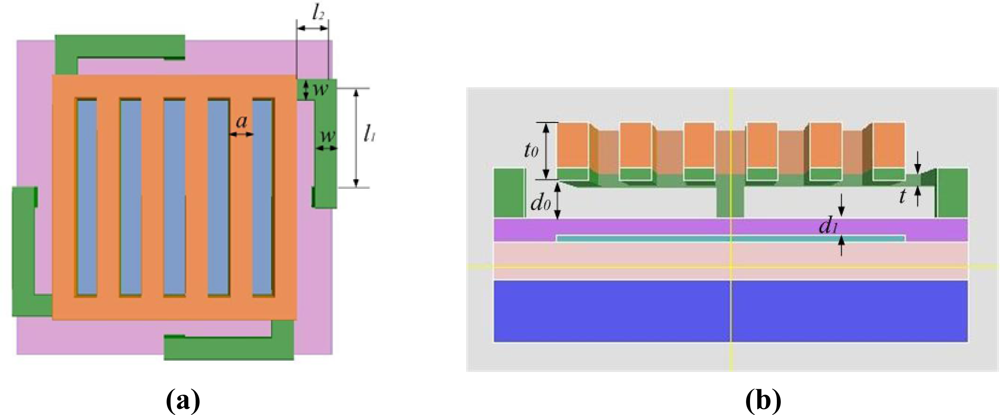
2. The principle of GLM

Figure 1 shows the structure of a single GLM. It is consisted of silicon substrate, bottom reflector, silicon dioxide, cantilever beam and movable grating.
Both the movable grating and the bottom reflector are made of aluminum, and they are separated by an insulating layer and an air gap. The movable grating and the bottom reflector form a phase grating, and the phase difference is determined by the space between the movable grating and the bottom reflector.
In Figure 2, when no voltage is applied between the movable grating and the bottom reflector, the phase difference of the GLM equals to (2n'+1)π (n' is a positive integer), and the diffraction light is mainly focused on the ±1st order. When a voltage is actuated between them, the electrostatic force pulls the movable grating downwards. The phase difference equals to 2n'π, and the diffraction light is mainly focused on the zero order. The switch between the dark state and the bright state can be realized by collecting the zero order or the ±1st order diffraction light. Figure 3 shows the diffraction intensity distributions of the GLM when the phase difference is 2n'π or (2n'+1)π.
Passive matrix addressing for the GLM is composed of a horizontal electrode group and a vertical electrode group. Every GLM’s bottom reflector in a row connects to a horizontal electrode which produces a row pulse signal, and every GLM’s movable grating in a column connects to a vertical electrode which is taken as a data line. When all horizontal electrodes are scanned by the progressive mode, a frame image can be displayed by a GLM array. Figure 4 shows a SEM photograph of the fabricated 16×16 GLM array addressed by passive matrix.

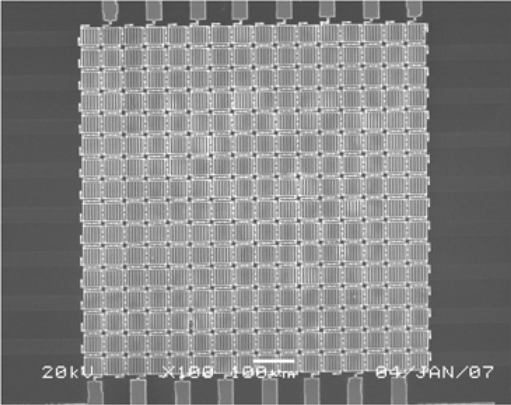
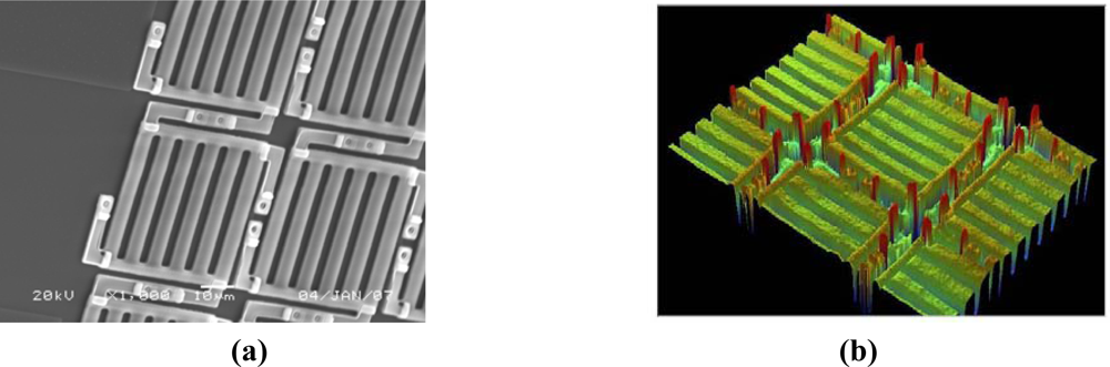
3. Device fabrication

The GLM fabrication process [8] is shown in Figure 5. The fabrication begins with a <100> p-type silicon wafer made using surface micro-machining technology. For electrical isolation among bottom electrode, 600 nm thick thermal silicon dioxide is deposited. Then 100 nm aluminum is sputtered and patterned to make the bottom reflector. Next, 280 nm silicon dioxide was deposited as a dielectric layer by PECVD.
After the formation of SiO2 layer, 580 nm polyimide (PI) is spin-coated as a sacrificial layer, and four support post cavities are etched by plasma on the sacrificial layer. Then 200 nm aluminum is sputtered, and four support cavities are filled with aluminum. Then, the photoresist (PR) is spin-coated as a protection layer and exposed, and another 530 nm aluminum is sputtered. Two aluminum layers are lithographed to form the upper movable grating, and the aluminum under PR is formed to cantilever beam. Finally, both PI and PR are etched by plasma at the same time. Figure 6a shows the SEM photograph of one corner of the fabricated 16×16 array. The width of the movable grating ribbon is 4 μm, the grating constant of the movable grating is 8μm, and the size of a single GLM is 52 × 52 µm. The residual stress σ of the cantilever beam measured by the MEMS foundry is equal to about 100 Mpa[8]. Figure 6b is a photograph of parts of the GLM array by VEECO. Figure 6 indicates that the surface of the movable grating is quite smooth.

4. Theoretical analysis of the GLM’s electromechanical characteristics

The motion of the movable grating is determined by the electrostatic force and the mechanical restoring force. The movable grating and the bottom reflector can be considered as a variable plane-parallel capacitor. The thickness of the cantilever beam using a buried-beam process is quite thin. The thickness of the movable grating is much thicker than the cantilever beam, as shown in Figure 7, where l1 and l2 are the two part lengths of the cantilever beam, t is the thickness of the cantilever beam, w is the width of the cantilever beam, d0 is the initial space between the movable grating and the dielectric layer, and d1 is the thickness of the dielectric layer. When the GLM is actuated by a voltage, the movable grating will pull down rigidly. The movable grating can be considered as a rigid body, so the spring constant of the movable grating can be ignored. A cantilever beam is taken as a spring, and the four cantilever beams are equivalent to the four shunt springs. Therefore, the GLM can be described as the capacitor-spring model.
The response frequency which affects the grayscale of the passive matrix GLM is a key parameter. The faster the response frequency is, the larger the grayscale is. The driving voltage is also a key parameter for the passive matrix GLM, and the lower driving voltage can decrease the complexity and power in system control circuits. The fabricated GLM should have high response frequency and low driving voltage characteristics. Furthermore, the passive matrix addressing for the GLM results to the crosstalk which will reduce the contrast and the light utilization of the GLM.

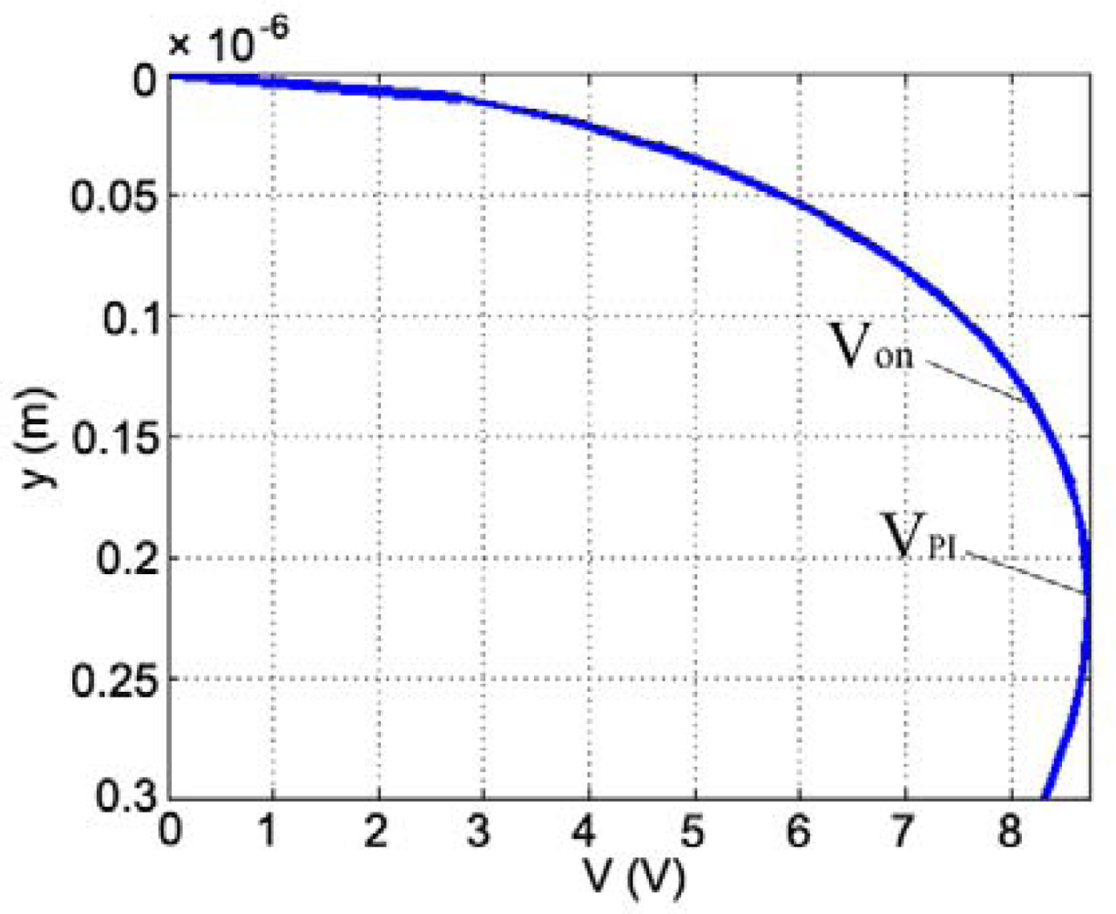
4.1. Response frequency and driving voltage

The resonant frequency w0 equals to k / m [10], where m is the effective mass of the movable grating and k is the spring constant of the GLM. If the spring constant is larger, the response frequency is faster. The driving voltage of the GLM is obtained as [8]:
V = ( d 0 + d 1 ε 1 y ) 2 ky ε ε 0 γ A
where A is the area of the movable grating, y is the displacement of the movable grating, γ is a correctional factor, ε1 is the relative dielectric constant of the dielectric layer, and ε which is the relative dielectric constant of the air equals to 1.
The initial phase difference of the designed GLM is (2n'+1)π. When a voltage is applied on the GLM, the electrostatic force pulls the movable grating down. If y is λ/4(λ is the wavelength of incident light), the phase difference becomes 2n'π, and this driving voltage is called the operating voltage of the GLM. If y is 1 3 ( d 0 + d 1 / ε 1 ), the electrostatic force is much larger than the mechanical restoring force, the movable grating will pull in, and this driving voltage is called the pull-in voltage of the GLM. According to the analysis above, it is indicated that the spring constant of the GLM is larger, and both the response frequency and the driving voltage are larger. In equation (1), the spring constant k of the GLM is only an unknown variable, so it is necessary to analyze the spring constant of the GLM.
The spring constant k’ of a cantilever beam which is determined by the structure parameter and the material characteristic of the cantilever beam is composed of two spring constants. k’ is the sum of k1 and k2. Where k1 results from the stiffness of the cantilever beam, and k2 is caused by the residual stress. First, the spring constant k1 can be written as [9, 10]:
k 1 = Ew ( t l 2 ) 3 1 + l 1 l 2 [ ( l 1 l 2 ) 2 + 12 1 + v 1 + ( w t ) 2 ]
where σ is the residual stress of the cantilever beam, v is Poisson ratio, and E is Young modulus. Furthermore, the spring constant k2 can be obtained as [11]:
k 2 = σ ( 1 v ) t w 2 ( l 1 + l 2 )
Finally, because of four shunt cantilever beams, the spring constant of the GLM is the sum of the four cantilever beams’ spring constants, and it can be expressed as follows:
k = 4 ( k 1 + k 2 ) = 4 Ew ( t l 2 ) 3 1 + l 1 l 2 [ ( l 1 l 2 ) 2 + 12 1 + v 1 + ( w t ) 2 ] + 2 σ ( 1 v ) t w ( l 1 + l 2 )
According to equation (4) and Table 1, k equals to 16.1758 N/m. Substitute the correlative parameters into equation (1), the relationship of the displacement y and the driving voltage V can be calculated, as shown in Figure 8. When y is 133 nm (λ/4, λ=532 nm), the operating voltage Von is 8.16 V; when y is 217.3 nm ( 1 3 ( d 0 + d 1 / ε 1 )), and the pull-in voltage VPI is 8.74 V.

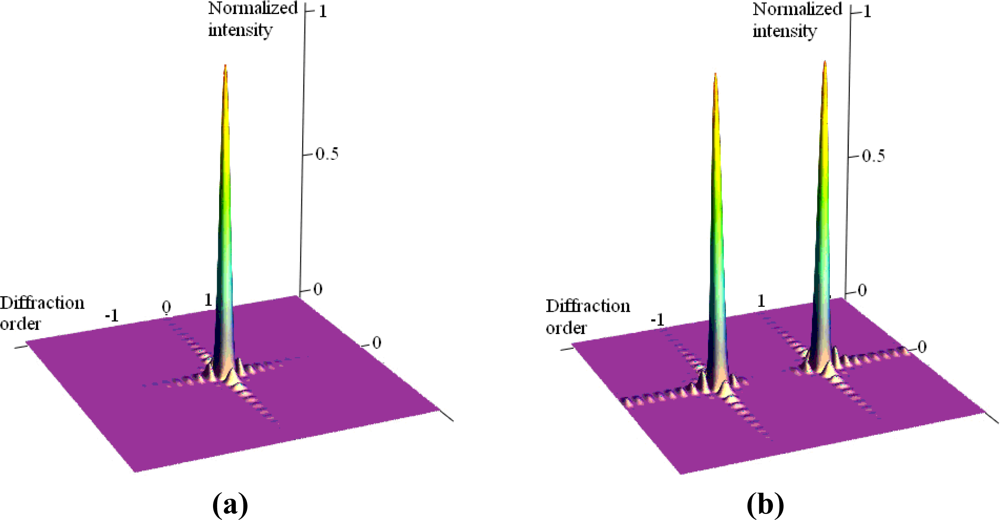
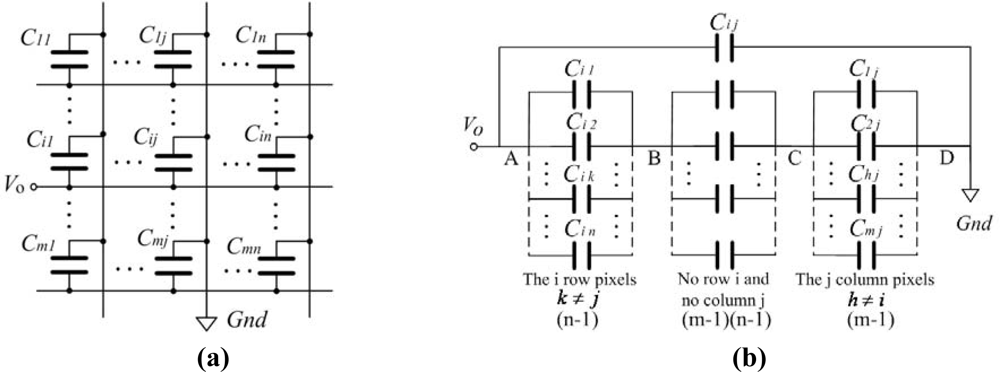
4.2. Analysis of crosstalk in the GLM array

The GLM can be equivalent to a capacitor Cg which can be expressed as follows [8]:
C g = ε ε 0 A h [ 1 + h π a + h π a ln ( 2 π a h ) + h π a ln ( 1 + 2 t 0 h + 2 t 0 h + t 0 2 h 2 ) ]
where a is the width of the movable grating ribbon, t0 is the thickness of the movable grating as shown in Figure 7, and h is the equivalent distance which equals to (d0+d11−y).
A passive matrix addressing for the GLM causes the matrix capacitance’s coupling effect which is also called crosstalk. In a m×n GLM array, a voltage V0 is applied on the cross pixel of the i row and the j column, and this cross pixel is called all-selected pixel, as shown in Figure 9a. The other pixels in the i row and the j column are called half-selected pixel, and the rest pixels in the array are called non-selected pixel.
It’s supposed that the initial voltages of all pixels are zero. By using Kirchhoff’s current law(KCL)and Kirchhoff’s voltage law(KVL)[15], Figure 9b can be simplified from Figure 9a. Where VAB is the voltage of the half-selected pixel in the all-selected pixel row, VCD is the voltage of the half-selected pixel in the all-selected pixel column, and VBC is the voltage of the non-selected pixel. According to Figure 9b, the relationship of the different voltages can be obtained as:
{ V BC   ( t ) = C AB C BC V AB   ( t ) V CD   ( t ) = C AB C CD V AB   ( t ) V AB + V BC + V CD = V 0
Every GLM is the same in the GLM array, so the capacitance value of every GLM is the same:
{ C AB = ( n 1 ) C g C BC = ( m 1 ) ( n 1 ) C g C CD = ( n 1 ) C g
Taking equation (7) into (6), the voltages of the different pixels can be given by:
{ V AB = m 1 m + n 1 V 0 V CD = n 1 m + n 1 V 0 V BC = 1 m + n 1 V 0
From equation (8), its shown that the voltage of the half-selected pixel is smaller than that of the total-select pixel, but its much bigger than that of the non-selected pixel. If the GLM array is larger, the crosstalk is more serious. As the 16×16 array, the voltages of the half-selected pixel and the non-selected pixel are 15/31(about 1/2) and 1/31 times respectively of the voltage of the total-select pixel.
A single GLM is actuated by a voltage, which results in the crosstalk in the GLM array. When the GLM array is scanned by the progressive mode, there may be lots of pixels which are actuated by the different voltages at the same time. It can be analyzed by the same method as before. The voltages of the half-selected pixel and the non-selected pixel may be different, but the crosstalk is more obvious. So the GLM array addressed by passive matrix can be applied in projection display with a low resolution and a low definition.

5. Experiments

Figure 10 shows the testing system of the passive matrix addressing for the GLM array. It is consisted of a light source, a 16×16 GLM array, a high-voltage driver, a signal generator, an aperture, a projection lens, a photoelectric diode, a current amplifier and an oscilloscope. The 16×16 GLM array is controlled by the high-voltage driver and the signal generator. A green laser is diffracted by the GLM array, and only the ±1st order diffraction light is passed by the aperture. Then, the ±1st order diffraction light passes the projection lens and displays an image of the GLM array. Only a single GLM pixel enters the photoelectric diode. The light intensity of the ±1st order diffraction can be converted to a photocurrent by the photoelectric diode. This photocurrent is amplified and converted to a voltage signal by the current amplifier, and this voltage signal is displayed on the oscilloscope.

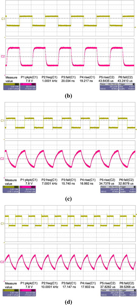
5.1. Results of driving voltage and response frequency

In Figure 11, the upper curve “C1” is the driving voltage of the GLM, and the bottom curve “C2” is the ±1st order intensity response of the GLM. Figure 11a shows that the GLM is actuated by a ramp-wave voltage. The ±1st order initial phase difference of the fabricated GLM is (2n'+1)π. According to the operating principle of the GLM, when no voltage is applied, the intensity of the ±1st order diffraction light is the bright state, and a high voltage signal is read out on the oscilloscope. When the ramp-wave voltage increases slowly, the movable grating moves down slowly, the intensity of the ±1st order diffraction light will decrease, and the voltage signal of the ±1st order diffraction light on the oscilloscope reduces. When the movable grating moves down a λ/4 distance, the phase difference become 2n'π, and the light intensity is in a minimum which is the dark state. As a result of the phase’s period, the ramp-wave voltage continues to increase, the light intensity increases, but as the movable grating pulls in, the light intensity jumps to a maximum. Figure 11a shows that the operating voltage Von of the GLM is 7.8 V and the pull-in voltage VPI of the GLM is 8.5 V, which are very close to the theoretical values. The difference between the theoretical value and the experimental value results from the slight difference between the designed structure and the fabricated structure.
Figures 11b, 11c and 11d are the ±1st order light intensity responses of the GLM actuated by the square-wave voltages of 7.8 V and different frequencies. For a half period, no voltage is actuated on the GLM, and the light intensity is in the maximum. For the other half period, a 7.8 V voltage is actuated on the GLM, and the light intensity is in the minimum. Figure 11b shows that the GLM works well at 1 kHz frequency, and the rise time and the fall time of the intensity response are about 43.64 μs and 43.24 μs, respectively. Figure 11c indicates that when the frequency is 7 kHz, the intensity response wave is distorted. And when the frequency is 10 kHz, the intensity response wave gets attenuated obviously, as seen in Figure 11d. The results indicate that the response frequency of the GLM is about 7 kHz.

5.2. Results of the crosstalk

In Figure 12, the upper curve “1” is the square-wave voltage of the all-selected pixel, and the bottom curve “2” is the ±1st order diffraction light intensity of the different pixels. As the fabrication processes of all pixels in array are the same, the pixels with the same peak-to-peak value of the diffraction light intensity have the same actuated voltage in the same scope of the phase difference. By comparing Figure 12a with Figure 12e, the peak-to-peak value of the light intensity is 280 mV when the square-wave voltage of the all-selected pixel is 1V, which is very approximate to 250 mV when the square-wave voltage of the all-selected pixel is 2 V. It can be concluded that the square-wave voltage of the half-selected pixel in Figure 12e is about 1V, which is consistent to the theory that the voltage of the half-selected pixel is half of the all-selected pixel in the 16×16 GLM array. The results also show that when an all-selected pixel is actuated by a voltage, the voltage of the half-selected pixel is much larger than the voltage of the non-selected pixel, but it is smaller the voltage of the all-selected pixel, which agrees with the crosstalk theory of the matrix capacitance.
The ±1st order diffraction intensities of the different pixels when an all-selected pixel is actuated by 1 V to 6 V square-wave voltages are shown in Figure 13. The results indicate that the peak-to-peak values of those three pixels all increase when the voltage of the all-selected pixel increases. Using the same analysis as before, it is shown that in the 16×16 GLM array the voltage of the half-selected pixel is half of the all-selected pixel, and the non-selected pixel voltage is quite small, which also agrees with the theoretical analysis.

6. Conclusions

The operating theory of passive matrix addressing for GLM is introduced in this paper. The response frequency and the driving voltage of the GLM are analyzed, and the crosstalk which influences the performance of the GLM array is also studied in detail. It is concluded that: (1) both the response frequency and the driving voltage are related to the spring constant of the GLM. The theoretical operating voltage and the pull-in voltage are 8.16 V and 8.74 V respectively; (2) in a GLM array, the half-selected pixel voltage is half of the all-selected pixel in an array, and the voltage of the half-selected pixel is much larger than that of the non-selected pixel. With the increase of the GLM array, the crosstalk becomes more serious; (3) the experimental results indicate that the operating voltage and the pull-in voltage are 7.8 V and 8.5 V, respectively, very close to their theoretical values. When the GLM is actuated by a square-wave voltage of 7.8 V and 1 kHz frequency, the rise and the fall times of the intensity response are about 43.64 μs and 43.24 μs, respectively. The response frequency of the GLM is about 7 kHz. Another experiment confirms the crosstalk in the GLM array. A GLM array addressed by passive matrix can be applied in low resolution and low definition projection displays. These studies can provide a theoretical basis for improving the driving characteristic of the GLM. In future, in order to eliminate the crosstalk of passive matrix addressing for GLM, we are planning to use an active matrix method in driving the GLM array, which can be applied in projection display with high resolution and high definition.

Acknowledgments

The authors thank the anonymous reviewers for their suggestions, which greatly improve the paper. This work was supported by National Natural Science Foundation of China (No. 60708017) and Academician Foundation of Chongqing in China (CSTC, 2008BC3002).

References and Notes

  1. Wu, M.C.; Solgaard, O.; Ford, J.E. Optical MEMS for lightwave communication. Journal of Lightwave Technology 2006, 24, 4433–4453. [Google Scholar]
  2. Tamada, H.; Taguchi, A.; Oniki, K. High contrast and efficient blazed Grating Light Valve for Full-HD 5,000lumen laser projectors. Digest of Technical Papers ICCE2006 2006, 133–134. [Google Scholar]
  3. Kim, S.; Barbastathis, G.; Tuller, H.L. MEMS for Optical Functionality. Journal of Electroceramics 2004, 12, 133–144. [Google Scholar]
  4. Hornbeck, L.J. Digital Light Processing TM for high brightness, high-resolution applications. Proc. SPIE, Projection Displays III 1997, 3013, 27–40. [Google Scholar]
  5. Bloom, D.M. The Grating Light Valve: revolutionizing display technology. Proc. SPIE, Projection Displays III 1997, 3013, 165–171. [Google Scholar]
  6. Sun, J.Y.; Huang, S.L. Two-dimensional grating light modulator for projection display. Applied Optics 2008, 15, 2813–2820. [Google Scholar]
  7. Zhang, J.; Huang, S.L. Optimization and analysis for structural parameters of Grating Moving Light Modulator. Acta Optica Sinica 2006, 26, 1121–1126. [Google Scholar]
  8. Zhang, Z.H. Study on some key technologies of MOEMS-based Grating Moving Light Modulator array, Ph. D. Thesis,. Chongqing University, Chong Qing, P.R. China, 2008; pp. 22–26.
  9. Yun, W.J. A surface micromachined accelerometer with integrated CMOS Detection Circuitry, Ph. D. Thesis,. University of California at Berkeley, Berkeley, CA, USA, 1992; pp. 78–84.
  10. Huang, Q.A.; Liao, X.P. RF MEMS Theory, Design, and Technology; Publishing House of Southeast University: Nan Jing, P.R. China, 2005; pp. 26–27. [Google Scholar]
  11. Lin, T.H. Implementation and characterization of a flexure-beam micromechanical spatial light modulator. Optical Engineering 1994, 33, 3643–3648. [Google Scholar]
  12. Aliev, A.E.; Shin, H.W. Image diffusion and cross-talk in passive matrix electrochromic displays. Displays 2002, 23, 239–247. [Google Scholar]
  13. Braun, D.; Rowe, J. Crosstalk and image uniformity in passive matrix polymer LED displays. Synthetic Metals 1999, 102, 920–921. [Google Scholar]
  14. Seuntiens, P.J.H.; Meesters, L.M.J. Perceptual attributes of crosstalk in 3D images. Displays 2005, 26, 177–183. [Google Scholar]
  15. Cai, W.J. Circuits theory; Zhejiang University Press: Zhe Jiang, P.R. China, 2006; pp. 11–13. [Google Scholar]
  16. Ying, G.Y.; Hu, W.B. Flat display technology; Post & Telecommunications Press: Bei Jing, P.R. China, 2002; pp. 193–200. [Google Scholar]
  17. Stephen, D.S. Microsystem Design; Publishing House of Electronics Industry: Bei Jing, P.R. China, 2004; pp. 123–150. [Google Scholar]
Figure 1. The structure of a single GLM.
Sensors 09 02162f1
Figure 2. The operating principle of the GLM.
Sensors 09 02162f2
Figure 3. The diffraction intensity distribution of the GLM. (a) The phase difference is 2n'π. (b) The phase difference is (2n'+1)π.
Sensors 09 02162f3
Figure 4. A SEM photograph of passive matrix addressing for the 16×16 GLM array.
Sensors 09 02162f4
Figure 5. The fabrication process of GLM.
Sensors 09 02162f5
Figure 6. The photograph of the fabricated GLM array. (a) The SEM photograph of parts of a GLM array. (b) The VEECO photograph of parts of the fabricated GLM array.
Sensors 09 02162f6
Figure 7. The structure and the parameters of the GLM. (a) The top image; (b) The cross-section image.
Sensors 09 02162f7
Figure 8. The simulation of the displacement and the driving voltage.
Sensors 09 02162f8
Figure 9. The matrix capacitance model of a m×n GLM array. (a) The initial model. (b) The simplified model.
Sensors 09 02162f9
Figure 10. The experimental system. (a) The sketch diagram of the experimental system. (b) The actual experimental system.
Sensors 09 02162f10
Figure 11. The testing results of the ±1st order diffraction light. (a) The intensity response of the GLM actuated by a ramp-wave. (b) The intensity response of the GLM actuated by a square-wave of 7.8 V and 1 kHz frequency. (c) The intensity response of the GLM actuated by a square-wave of 7.8 V and 7 kHz frequency. (d) The intensity response of the GLM actuated by a square-wave of 7.8 V and 10 kHz frequency.
Sensors 09 02162f11aSensors 09 02162f11b
Figure 12. The ±1st order diffraction light intensities of the different pixels when an all-selected pixel is actuated by different square-waves. (a) all-selected pixel when actuated by a 1V square-wave. (b) half-selected pixel when an all-selected pixel is actuated by a 1V square-wave. (c) non-selected pixel when an all-selected pixel is actuated by a 1V square-wave. (d) all-selected pixel when actuated by a 2 V square-wave. (e) half-selected pixel when an all-selected pixel is actuated by a 2V square-wave. (f) non-selected pixel when an all-selected pixel is actuated by a 2V square-wave.
Sensors 09 02162f12
Figure 13. The ±1st order diffraction light intensity of different pixels when an all-selected pixel is actuated by 1V to 6V square-waves voltages.
Sensors 09 02162f13
Table 1. The correlative parameters of the designed GLM [8].
d1 (μm)ε1ε0 (F/m)d0 (μm)γA (μm2)t (μm)w (μm)l1 (μm)l2 (μm)E (Gpa)vσ (Mpa)
0.283.98.854 × 10−120.581.2815330.24.010.53.5770.3100

