A MEMS-based Benzene Gas Sensor with a Self-heating WO3 Sensing Layer

Abstract
:1. Introduction
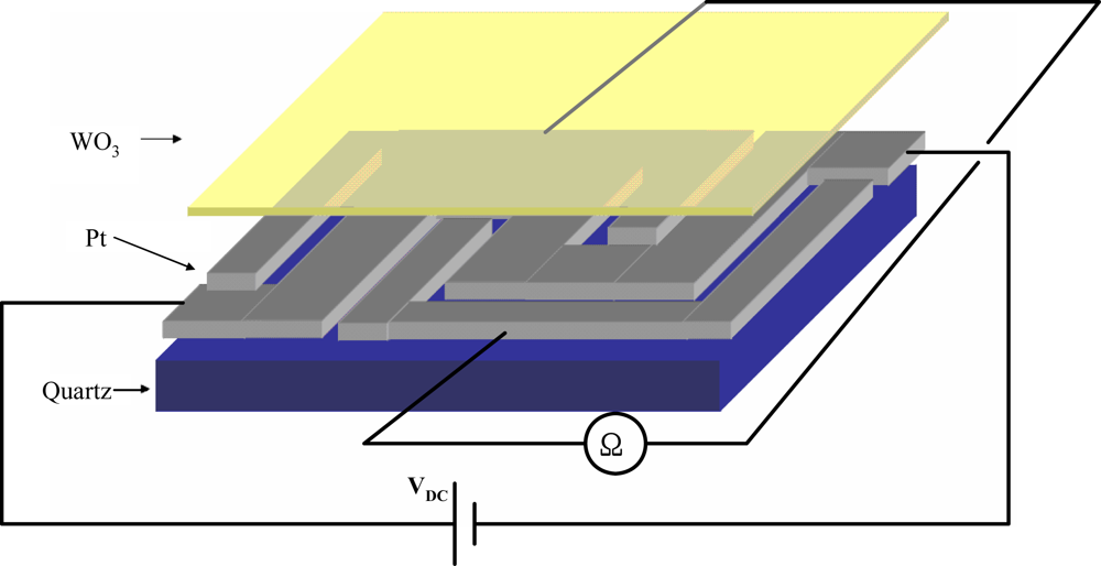
2. Sensor Design
2.1. Micro-heater
2.2. Design
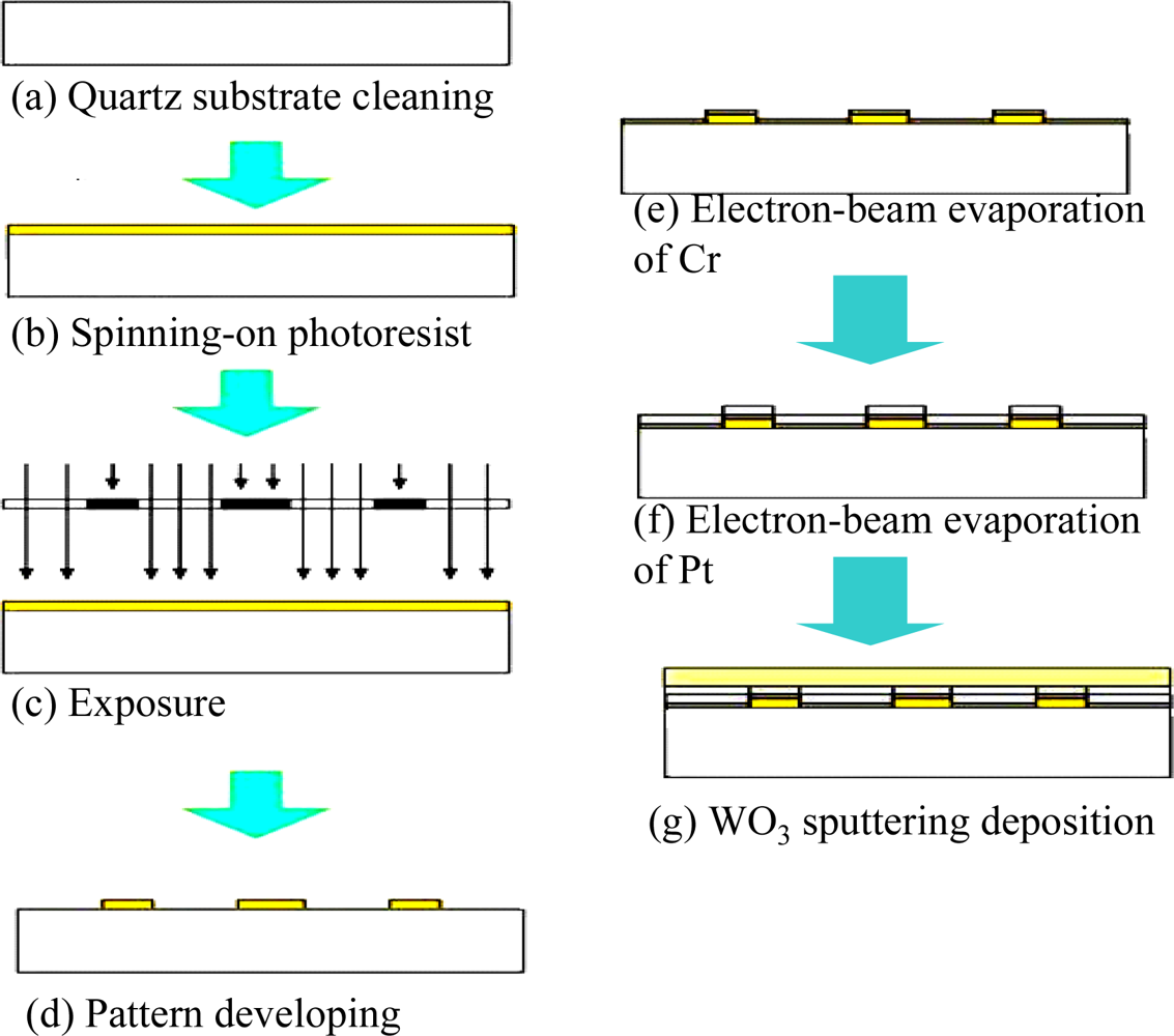
3. Fabrication
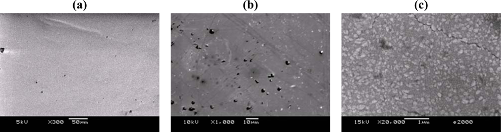
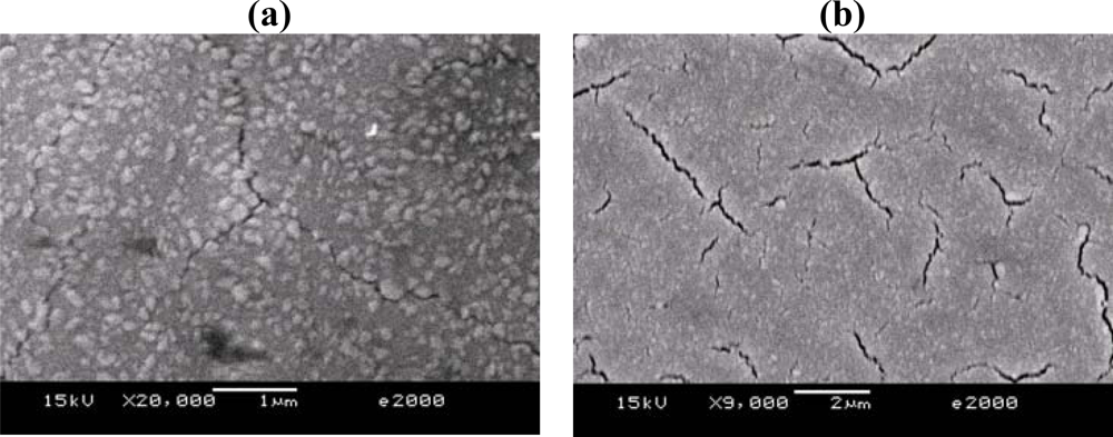
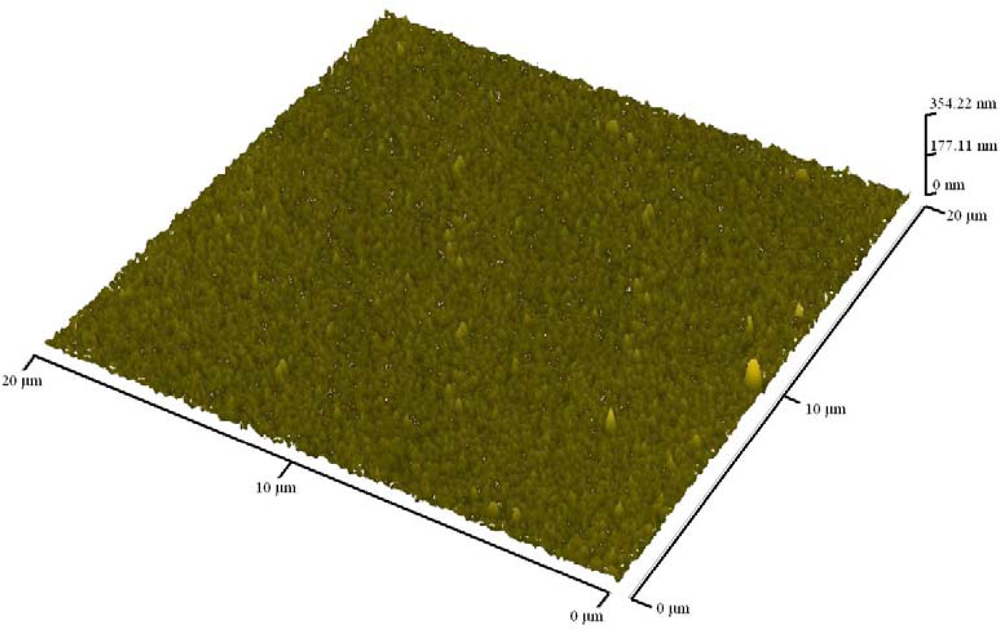
3.1. Thin film deposition
3.2. Microfabrication
4. Results and Discussion
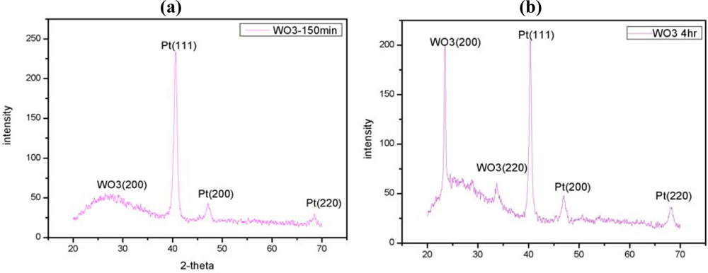
4.1. Diffraction pattern of WO3 thin-film layer
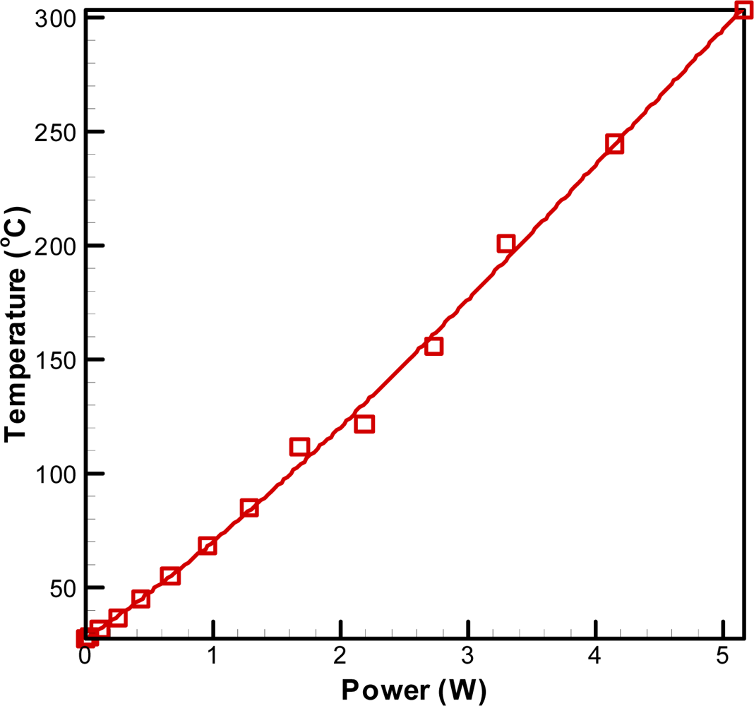
4.2. Effect of applied power on micro-heater temperature
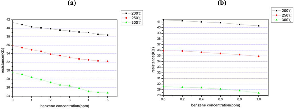
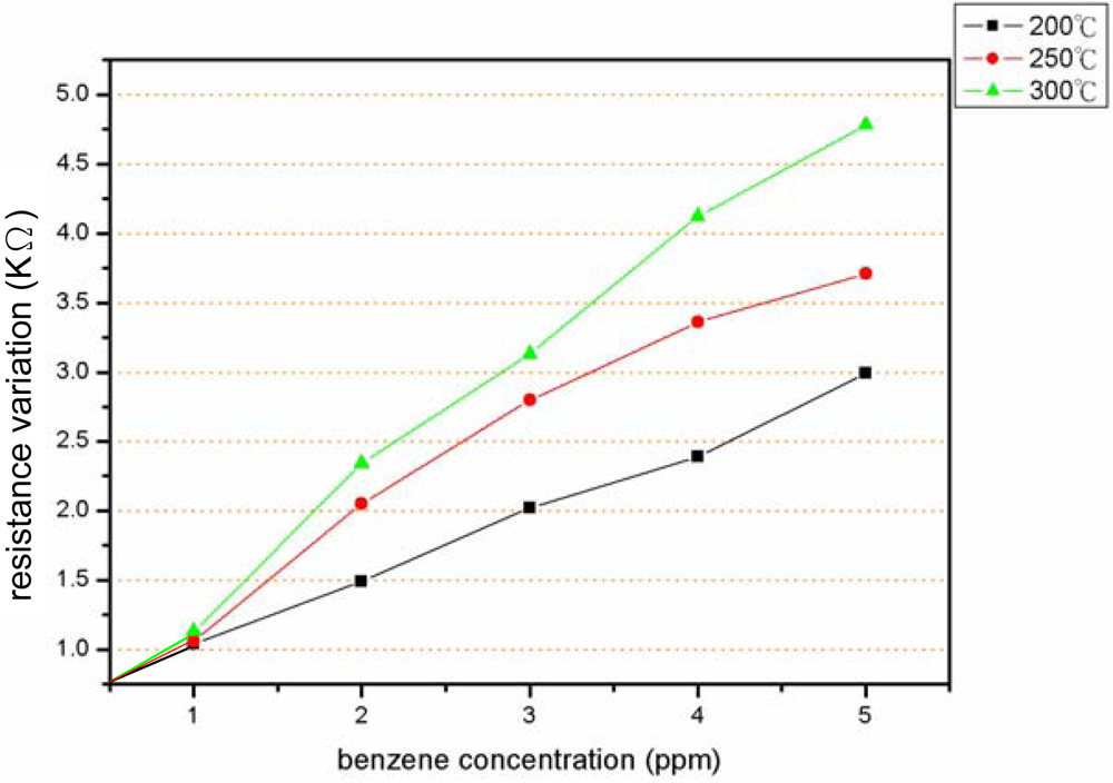
4.3. Benzene concentration sensitivity
4.4. Time response
4.5. Repeatability
4. Conclusions
Acknowledgments
References
- Cometto-Muňiz, J.E.; Cain, W.S.; Abraham, M.H. Detection of single and mixed VOCs by small and by sensory irritation. Indoor Air 2004, 14, 108–117. [Google Scholar]
- Hubálek, J.; Malysz, K.; Prášek, J.; Vilanova, X.; Ivanov, P.; Llobet, E.; Brezmes, J.; Correig, X.; Svěrák, Z. Pt-loaded Al2O3 catalytic filters for screen-printed WO3 sensors highly selective to benzene. Sens. Actuat. B Chem 2004, 101, 277–283. [Google Scholar]
- Mine, Y.; Melander, N.; Richter, D.; Lancaster, D.G.; Petrov, K.P.; Curl, R.F.; Tittel, F.K. 1997 Detection of formaldehyde using mid-infrared difference-frequency generation. Appl. Phys. B 1997, 65, 771–774. [Google Scholar]
- Friedfeld, S.; Fraser, M. Field intercomparison of a novel optical sensor for formaldehyde quantification. Geophys. Res. Lett 2000, 27, 2093–2096. [Google Scholar]
- Richter, D.; Fried, A.; Wert, B.P.; Walega, J.G.; Tittel, F.K. Development of a tunable mid-IR difference frequency laser source for highly sensitive airborne trace gas detection. Appl. Phys. B 2002, 75, 281–288. [Google Scholar]
- Podola, B.; Nowack, E.C.M.; Melkonian, M. The use of multiple-strain algal sensor chips for the detection and identification of volatile organic compounds. Biosens. Bioelectron 2004, 19, 1253–1260. [Google Scholar]
- Liewhiran, C.; Phanichphant, S. Influence of thickness on ethanol sensing characteristics of doctor-bladed thick film from flame-made ZnO nanoparticles. Sensors 2007, 7, 185–201. [Google Scholar]
- Reungchaiwat, A.; Wongchanapiboon, T.; Liawruangrath, S.; Phanichphant, S. Home-made detection device for a mixture of ethanol and acetone. Sensors 2007, 7, 202–213. [Google Scholar]
- Sadek, K.; Moussa, W. Studying the effect of deposition conditions on the performance and reliability of MEMS gas sensors. Sensors 2007, 7, 319–340. [Google Scholar]
- Liewhiran, C.; Phanichphant, S. Effects of palladium loading on the response of a thick film flame-made ZnO gas sensor for detection of ethanol vapor. Sensors 2007, 7, 1159–1184. [Google Scholar]
- Sahner, K.; Gouma, P.; Moos, R. Electrodeposited and sol-gel precipitated p-type SrTi1−xFexO3−δ semiconductors for gas sensing. Sensors 2007, 7, 1871–1886. [Google Scholar]
- Wang, Y.H.; Lee, C.Y.; Chiang, C.M. A MEMS-based air flow sensor with a free-standing micro-cantilever structure. Sensors 2007, 7, 2389–2401. [Google Scholar]
- Wang, X.; Carey, W.P.; Yee, S.S. 1995 Monolithic thin-film metal-oxide gas-sensor arrays with application to monitoring of organic vapors. Sens. Actuat. B Chem 1995, 28, 63–70. [Google Scholar]
- Tomchenko, A.A.; Khatko, V.V.; Emelianov, I.L. WO3 thick-film gas sensors. Sens. Actuat. B Chem 1998, 46, 8–14. [Google Scholar]
- Tomchenko, A.A.; Emelianov, I.L.; Khatko, V.V. Tungsten trioxide-based thick-film NO sensor: design and investigation. Sens. Actuat. B Chem 1999, 57, 166–170. [Google Scholar]
- Penza, M.; Tagliente, M.A.; Mirenghi, L.; Gerardi, C.; Matucci, C.; Cassano, G. Tungsten trioxide (WO3) sputtered thin film for a NOx gas sensor. Sens. Actuat. B Chem 1998, 50, 9–18. [Google Scholar]
- Manno, D.; Serra, A.; Giulio, M.D.; Micocci, G.; Tepore, A. 1998 Physical and structural characterization of tungsten oxide thin films for NO gas detection. Thin Solid Films 1998, 324, 44–51. [Google Scholar]
- Lee, D.S.; Han, S.D.; Huh, J.S.; Lee, D.D. Nitrogen oxides-sensing characteristics of WO3-based nanocrystaline thick film gas sensor. Sens. Actuat. B Chem 1999, 60, 57–63. [Google Scholar]
- Llobet, E.; Molas, G.; Molinàs, P.; Calderer, J.; Vilanova, X.; Brezmes, J.; Sueiras, J.E.; Correig, X. Fabrication of highly selective tungsten oxide ammonia sensors. J. Electrochem. Soc 2000, 147, 776–779. [Google Scholar]
- Williams, D.E.; Aliwell, S.R.; Pratt, K.F.E.; Caruana, D.J.; Jones, R.L.; Cox, R.A.; Hansford, G.M.; Halsall, J. Modelling the response of a tungsten oxide semiconductor as a gas sensor for the measurement of ozone. Meas. Sci. Technol 2002, 13, 923–931. [Google Scholar]
- Aguir, K.; Lemire, C.; Lollman, D.B.B. Electrical properties of reactively sputtered WO3 thin films as ozone gas sensor. Sens. Actuat. B Chem 2002, 84, 1–5. [Google Scholar]
- Cavicchi, R.E.; Suele, J.S. Fast temperature programmed sensing for micro-hotplate gas sensors. IEEE Electron. Dev. Lett 1995, 16, 286–288. [Google Scholar]
- Lee, C.Y.; Hsieh, P.R.; Lin, C.H.; Chou, P.C.; Fu, L.M.; Chiang, C.M. MEMS-based formaldehyde gas sensor integrated with a micro-plate. Microsyst. Technol 2006, 12, 893–898. [Google Scholar]
- Lemire, C.; Lollman, D.B.B.; Mohammad, A.A.; Gillet, E.; Aguir, K; Reactive, R.F. Magnetron sputtering deposition of WO3 thin films. Sens. Actuat. B Chem 2002, 84, 43–48. [Google Scholar]
- Bendahan, M.; Roulmani, R.; Seguin, J.L.; Aguir, K. Characterization of ozone sensors based on WO3 reactively sputtered films: influence of O2 concentration in the sputtering gas, and working temperature. Sens. Actuat. B Chem. 2004, 100, 320–324. [Google Scholar]
- Labidi, A.; Jacolin, C.; Bendahan, M.; Abdelghani, A.; Guérin, J.; Aguir, K.; Maaref, M. Impedance spectroscopy on WO3 gas sensor. Sens. Actuat. B Chem 2005, 106, 713–718. [Google Scholar]
- Bittencourt, C.; Landers, R.; Llobet, E.; Molas, G.; Correig, X.; Silva, M.A.P.; Sueiras, J.E.; Calderer, J. Effects of oxygen partial pressure and annealing temperature on the formation of sputtered tungsten oxide films. J. Electrochem. Soc 2002, 149, H81–H86. [Google Scholar]
- Ivanov, P.; Hubalek, J.; Malysz, K.; Prášek, J.; Vilanova, X.; Llobet, E.; Correig, X. A route toward more selective and less humidity sensitive screen-printed SnO2 and WO3 gas sensitive layers. Sens. Actuat. B Chem 2004, 100, 221–227. [Google Scholar]


© 2009 by the authors; licensee MDPI, Basel, Switzerland This article is an open access article distributed under the terms and conditions of the Creative Commons Attribution license (http://creativecommons.org/licenses/by/3.0/).
Share and Cite
Ke, M.-T.; Lee, M.-T.; Lee, C.-Y.; Fu, L.-M. A MEMS-based Benzene Gas Sensor with a Self-heating WO3 Sensing Layer. Sensors 2009, 9, 2895-2906. https://doi.org/10.3390/s90402895
Ke M-T, Lee M-T, Lee C-Y, Fu L-M. A MEMS-based Benzene Gas Sensor with a Self-heating WO3 Sensing Layer. Sensors. 2009; 9(4):2895-2906. https://doi.org/10.3390/s90402895
Chicago/Turabian StyleKe, Ming-Tsun, Mu-Tsun Lee, Chia-Yen Lee, and Lung-Ming Fu. 2009. "A MEMS-based Benzene Gas Sensor with a Self-heating WO3 Sensing Layer" Sensors 9, no. 4: 2895-2906. https://doi.org/10.3390/s90402895