A New Control Method for a Bi-Directional Phase-Shift-Controlled DC-DC Converter with an Extended Load Range


1
Department of Electrical Engineering, The Hong Kong Polytechnic University, Hung Hom, Kowloon, Hong Kong, China
2
Hong Kong Branch of National Rail Transit Electrification and Automation Engineering Technology Research Center, Hong Kong, China
*
Author to whom correspondence should be addressed.
Energies 2017, 10(10), 1532; https://doi.org/10.3390/en10101532
Submission received: 21 July 2017
/
Revised: 29 September 2017
/
Accepted: 29 September 2017
/
Published: 10 October 2017
(This article belongs to the Special Issue Emerging Power Electronics Technologies for Power Systems and Machine Drives)
Abstract
:Phase-shifted converters are practically important to provide high conversion efficiencies through soft-switching techniques. However, the limitation on a resonant inductor current in the converters often leads to a non-fulfillment of the requirement of minimum load current. This paper presents a new power electronics control technique to enable the dual features of bi-directional power flow and an extended load range for soft-switching in phase-shift-controlled DC-DC converters. The proposed technique utilizes two identical full bridge converters and inverters in conjunction with a new control logic for gate-driving signals to facilitate both Zero Current Switching (ZCS) and Zero Voltage Switching (ZVS) in a single phase-shift-controlled DC-DC converter. The additional ZCS is designed for light load conditions at which the minimum load current cannot be attained. The bi-directional phase-shift-controlled DC-DC converter can implement the function of synchronous rectification. Its fast dynamic response allows for quick energy recovery during the regenerative braking of traction systems in electrified trains.
1. Introduction
The modern transportation industry focuses on railway electrification technology, which includes many advanced areas, such as materials, sensing, storage, and power electronics. With the rapid development of railway electrification and high speed railway technology, a lot of research areas including power electronics and materials are playing a more important role. Power electronics converters contribute to the bi-directional energy flowing from the traction grid and vehicles, as well as power flowing between different systems within a vehicle. Researchers have conducted lots of work to improve the performance including a high efficiency, less harmonics, and fast response. For example, the use of electric double layer capacitor sets for boosting voltages of contact lines in different kinds of railway traction systems is investigated [1] to better adopt the energy storage systems to reduce voltage drops and improve the stability. The popular wireless power transfer technology is also enhanced and utilized in high power applications, especially electric railway systems [2], where the power capacity, fast response, and reliability are all guaranteed. To meet the requirement of a high voltage conversion ratio with small ripples, an asymmetrical DC-DC converter is proposed [3] for fuel cell and solar energy applications. In certain new applications such as a microgrid, the coordinated control strategy of an interlink DC-AC converter is investigated to achieve high conversion efficiency [4] considering the state of charge of batteries and load shedding.
In the field of topology, a new three-phase to single-phase cascade converter in a traction substation is developed for the power supply system, which is based on three-level neutral point clamping and could match the capacity of the converter for a high voltage application [5]. A dual active bridge DC-DC converter with ZVS capacitors [6] was provided and tested in railway systems with a power level of 80 kW whose efficiency is quite high. Similarly, a proposed multi-resonant three-port bi-directional converter [7] could guarantee the ZVS of all switches by adjusting the driving frequency under different load conditions. A new bidirectional single stage full bridge topology with a high power factor and better dynamic characteristic is introduced which leads to small harmonics [8]. Similarly, a bidirectional topology of a non-inverting buck-boost converter is also investigated [9] in an islanded-mode microgrid. In the field of control, a new control signal generating methodology and predictive power control of converters [10,11] in an electrified railway system was proposed to limit the current harmonics of the grid with a fast response feature, as well as stabilizing the neutral point voltage. The voltage level and phase angle control methodology of the static converter is studied which has great potential for a railway system [12].
Since ZVS could minimize the switching losses of power switches, there are many resonant converters including a phase-shifted DC-DC converter [13,14,15] applying ZVS for the operations of power switches so as to increase the overall conversion efficiency. In [15], an adaptive phase shift control method was proposed with the automatic detection of load conditions and higher efficiency at light load compared to fixed phase shift control. However, the efficiency would undoubtedly drop with the output power level and is known to be poor at light load when fixed phase-shift control is adopted. Meanwhile, there is a minimum load constraint for those converters requiring the inductor current flowing through the active switch during the ZVS transition to be large enough in order to charge and discharge the energy stored in stray capacitances of resonant rank.
For the sake of minimizing the size of the resonant inductor used to store sufficient energy for the lagging leg of the inverter bridge to achieve ZVS under a light load condition, many different improvement methods have been proposed, for example, a combined phase-shift control algorithm and frequency modulation was proposed to achieve ZVS over the full load range in [16]; new control methods [17,18,19,20] were used for the converters under a light load condition to improve efficiency; a converter containing two paralleled half-bridge inverters and an auxiliary inductor on the primary side is proposed [21], which allows the stored energy for ZVS operation to change adaptively with duty-cycle and thus reduces the output filter inductance; phase-shift control with an L-C-L filter could also be utilized for ZVS to improve the performance [22]; DC link voltage was adjusted dynamically by power factor correction (PFC) in order to relieve the stress on semiconductor switches and improve the converter efficiency [23]; a two-stage isolated bi-directional DC-DC converter was investigated [24] which could enlarge the ZVS region by interleaving the converter with supercapacitors; dead-time for the lagging leg of the inverter bridge was adjusted predictively to assist the switches to perform ZVS at light load [25]; two additional switches were connected in parallel with the lagging leg of the inverter bridge to reduce switching loss under light load [26,27]; a novel ZCS-ZVS power factor correction PFC converter was proposed [28] with an efficiency of higher than 97%; two additional low-current diodes were added to the center-tap of a transformer secondary to improve ZVS at light load [29]; some other researchers proposed different control methods [30,31] and accomplished ZCS for the lagging leg, while retaining ZVS for the leading leg [31]. Improved ZVS techniques for the active switches of the forward converter are also adopted [32] in order to reduce switching and conducting losses to deal with PV power and wind energy. Although, the performance of these converters has been improved greatly, they cannot be used for applications requiring bi-directional power flow.
Other research works have been done to improve the load range problem for bi-directional phase-shifted converters, for instance, an active clamping branch with a Pulse Width Modulation (PWM) control algorithm was proposed to realize ZVS for all switches over a wide range of load [33,34]; a small inductor was proposed to be connected at the secondary of the power transformer to extend the load range [35]. These above-mentioned methods require either additional circuitries or complicated control logic.
In this paper, a new control method for a bi-directional phase-shift-controlled DC-DC converter is proposed. It can provide a path for reverse power flow and an extended load range for a light load condition without any supplementary circuitries. Furthermore, the proposed control method incorporates the gate drive logic for synchronous rectification so as to further improve the overall performance of the converter. A mathematical model is provided to demonstrate the principle and advantages of the proposed control method, including the linear output voltage with phase shift and achieving ZVS at light load. As the improved converter does have a fast dynamic response, it can be used for energy recovery during regenerative braking for the powertrain system of an electrified train, while high power density supercapacitors made of nano-/micro-structured materials are used as the energy storage.
Figure 1a presents a circuit topology of the proposed bi-directional phase-shift-controlled DC-DC converter which adopts ZCS in the left leg and ZVS in the right leg of the inverter-bridge so as to extend its load range to light load. The improved converter retains the bi-directional power flow capability with synchronous rectification [7,8,36] and offers linear output voltage control.
The topology of the improved converter consists of an inverter-bridge and a converter-bridge connected with a high-frequency power transformer K. As shown in Figure 1a, the inverter bridge is constructed with four MOSFETs, Q1–Q4, and the converter bridge is constructed with four MOSFETs, M1–M4. DQ1–DQ4 and DM1–DM4 are body diodes of MOSFETs, CQ1–CQ4, and CM1–CM4 are resonant capacitances that include the MOSFETs’ stray capacitance and other resonant capacitors. Lres is the resonant inductor that includes the total leakage inductance of the transformer and additional resonant inductor. Cin is the input filter capacitor and Co is the output filter capacitor. Rload is the load resistance. Driven with the proposed control logic, the converter can then operate in both directions and achieve soft-switching for an extended load range. The details of the control logic of gate drive signals will be described in the next section. In contrast, the secondary side of a conventional phase-shifted converter is a full bridge or half bridge rectifier composed of uncontrollable diodes, while there is a filter inductor in series with the output side, as shown in Figure 1b.
2. Analysis of the Circuit Operation
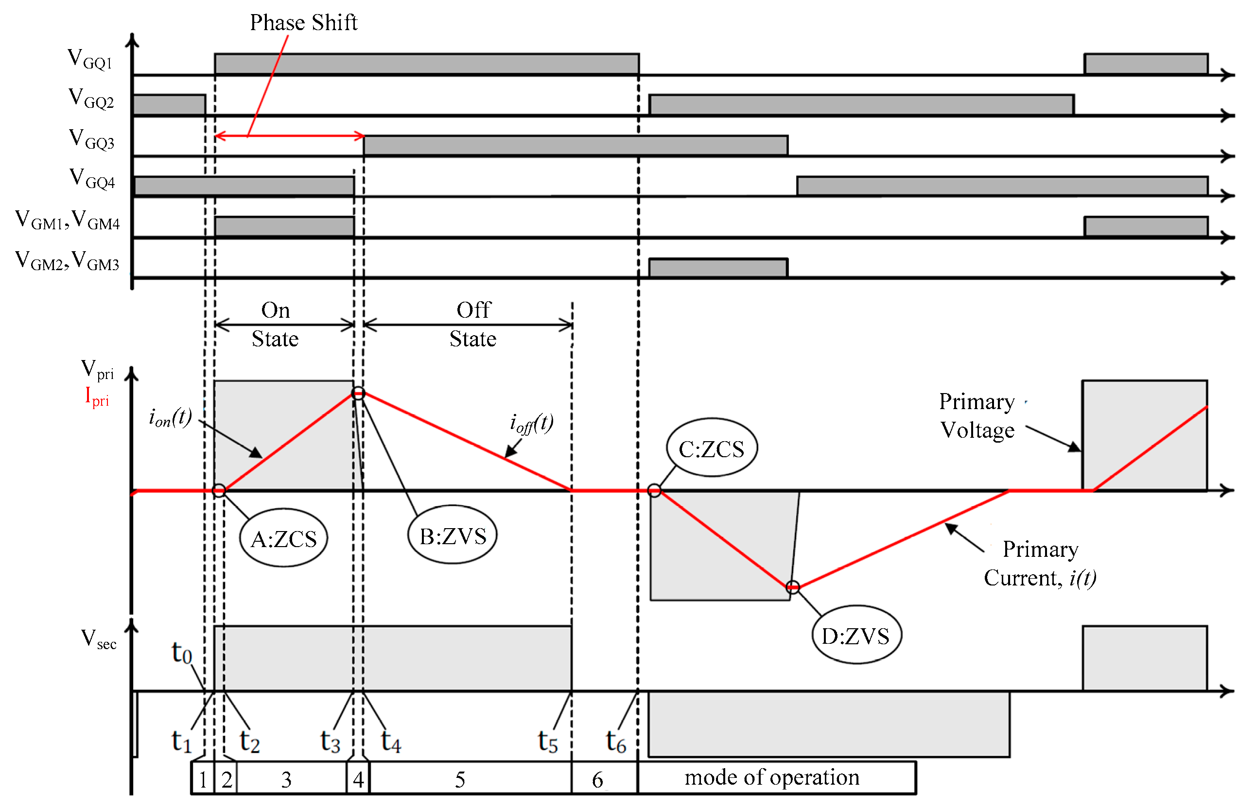
The improved converter employs a new control logic that can not only implement the phase-shift algorithm, but also provide bi-directional power flow control and synchronous rectification. Figure 2 illustrates the gate drive signals of the proposed control method, where VGQ1–VGQ4 and VGM1–VGM4 are the gate drive signals applied to Q1–Q4 and M1–M4, respectively, Vpri and Ipri represent the primary voltage and current, respectively, and Vsec represents the secondary voltage.
Circuit analysis of the improved converter will be focused on the light load condition, though it is equally applicable to the normal load condition where the converter would have similar characteristics as conventional phase-shifted topology, except that the output inductor is removed in the improved converter and therefore requires a higher resonant load current in order to achieve soft-switching. This is why the improved converter is aimed at the application with a very wide range of loading, such as energy storage for fluctuating sources.
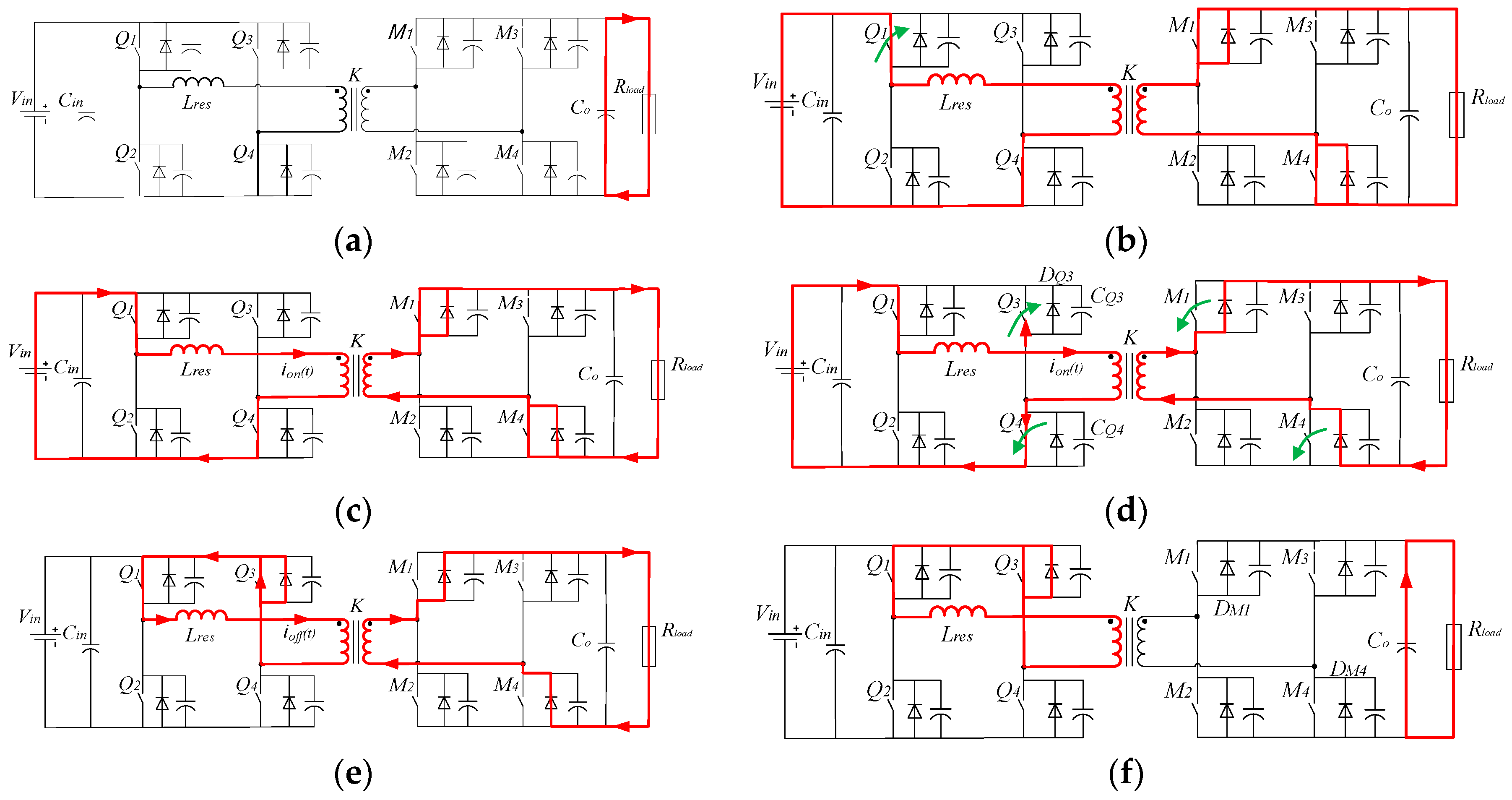
As the working principles of positive and negative half cycles are similar, only the positive half cycle is described, as shown in Figure 3. There are six modes in each half cycle.
Mode 1—Dead Time (t0 < t < t1)
M1–M4 are off. Q4 is on, and the transformer primary current i(t) is zero, Q3 is therefore turned off under ZCS. Energy stored in Co is delivered to Rload. The period of this mode is called dead-time, which is used to prevent Q1 and Q2 from shoot-through problems.
Mode 2—Left Leg ZCS Transition (t1 < t < t2)
Transformer primary current is still zero, and Q1 is therefore able to be turned on under ZCS. Simultaneously, M1 and M4 are also turned on under ZCS. Vin is then applied to the transformer primary, and its secondary is maintained at Vo.
Mode 3—Power Transferring (t2 < t < t3)
Q1, Q4, M1, and M4 keep conducting, while the primary side current is circulating as described by the function of ion(t). Detailed calculations will be given in the Mathematical Analysis of the Circuit.
Mode 4—Right Leg ZVS Transition (t3 < t < t4)
Q1 keeps conducting, and Q4 is now being turned off. Primary current ion(t) will charge up CQ4 and discharge CQ3 at the same time. When the voltage across CQ3 drops to zero, DQ3 is then conducting, and subsequently, Q3 can be turned on under ZVS. M1 and M4 will be turned off in this mode.
Mode 5—Freewheeling (t4 < t < t5)
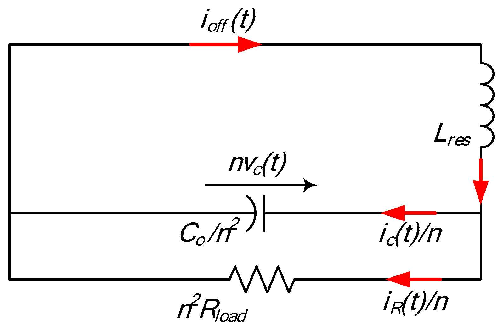
Q1 and Q3 remain on and there is no voltage at the primary side of the transformer. Meanwhile, energy stored in Lres is delivered to Rload through M1 and M4. The primary current is circulating as described by the function of ioff(t) (detailed calculations will be given in the Mathematical Analysis).
Mode 6 (t5 < t < t6)
Q1 and Q3 keep conducting, while the primary current reaches toward zero, then the body diodes DM1 and DM4 are reversely biased, which eventually isolates Co and Rload electrically. It is assumed that Co is sufficiently large, and therefore Vo can be maintained at a nearly constant rate.
3. Mathematical Analysis of the Circuits
In this section, a mathematical model will be developed, and it can be used to find out the extended load range at light load condition and the linear control region for the output voltage. This model includes the DC characteristics of the improved converter and load ranges for ZVS and ZCS.
Without a loss of accuracy for the circuit operation, the following assumptions were made in the derivation of mathematical equations:
- The improved converter has a very high conversion efficiency, so power loss is negligible, and this is generally acceptable for converters using a soft-switching technique that can effectively minimize the switching losses
- Output capacitor Co is sufficiently large to hold the converter output voltage at nearly constant
- Internal resistance of the transformer windings, inductors, and capacitors is negligible.
In addition, some common terms used for the calculations are defined in Table 1.
3.1. DC Characteristics
Derivation of the DC characteristics of the converter will be done based on the first assumption that power loss is negligible, so the input energy is equal to the output energy for the improved converter.
The converter only takes in energy from Vin in mode 3 of the operation (i.e., the power transferring stage), where t2 ≤ t ≤ t3, and t3 − t2 = DT/2. Figure 4a shows the input energy, Win during the power transferring stage, and the output energy of the converter for a half cycle is Wout, where:
and Ipeak represents the transformer’s peak primary-side current. As Win = Wout:
Figure 4b shows an equivalent circuit of the converter during this stage, where the definitions of relevant equations are listed in Table 2.
Then, the circuit model can be represented by:
Transformed into the s-domain, Equations (4)–(7) can be solved and the primary current Ion(s) is:
Then, taking an inverse Laplace transform, Equation (8) becomes:
where .
Assuming 4n2CoLresRload2 ≫ Lres2, 2n2CoRload2Vin ≫ LresVin, and 2CoRload ≪ 1, Equation (9) can be simplified as follows:
Putting into Equation (10), the peak primary current can be obtained as:
Substituting Equation (11) into Equation (3) yields the voltage conversion ratio of the improved converter, i.e.,
Since the output voltage of power transferring stage can be assumed as constant, the current waveform ion(t) can be regarded as a straight line and Ipeak can be obtained according to Equation (4) and Figure 4a as:
Substituting Equation (13) into Equation (3) to derive:
Solving Equation (14) to get the equation:
The voltage conversion ratio of the improved converter can be solved by Equation (15) and should match with the result given in Equation (12). A derivative of Equation (12) with respect to D is taken to check whether the output voltage can be controlled linearly proportional to the change of phase shift D, that is:
As the denominator of Equation (13) is always positive, an assumption can be made that the numerator of Equation (16) is also positive, i.e.,
Taking the square of both sides of Equation (17):
As inequality (18) is always true, the assumption holds, and will always be positive. This implies that the output voltage of the converter is a linear function of phase shift. This is particularly important for design engineers to design the feedback control system, because there is no special safeguard needed to limit the range of the control variable beyond a reverse control region as exhibited in the variable frequency resonant load converter.
3.2. Maximum Load Current for Left Leg to Achieve ZCS
Though, the improved converter can extend the load range with soft-switching for light load application, a design constraint does still exist as there is an upper limit of the transformer primary current for the left leg to achieve its ZCS.
Figure 5 illustrates four scenarios where the active switches of the left leg in the inverter bridge will encounter, where Ip represents the primary current of the transformer. In Figure 5a, it performs a ZCS as per our proposed method under a light load condition. In Figure 5b, it shows a marginal situation where ZCS is still achievable when the transformer primary current continues to increase. Once the primary current is higher than the marginal limit, the active switches cannot achieve ZCS. Moreover, if the primary current cannot meet the minimum load requirement of the conventional phase-shifted converter, these active switches are not able to perform ZVS, as illustrated in Figure 5c. When the load current meets the minimum load requirement, these active switches will operate with ZVS, as shown in Figure 5d.
Maximum load current IZCS(max) for the converter to maintain ZCS is a prerequisite parameter for system design. The following section will elaborate on the derivation of IZCS(max) in detail.
As shown in Figure 2, the transformer primary current decreases to zero during t4 ≤ t ≤ t5 (i.e., freewheeling stage), where t5 − t4 = kT/2, and k is a ratio of free-wheeling time over a half period of the switching cycle. Figure 6 shows the equivalent circuit for the active switch performing ZCS during the freewheeling stage, where ioff(t) is the transformer primary current. At t = t4, the energy stored in Lres is delivered to Rload, and the circuit operations can be described by the following equations:
Transformed into the s-domain, Equations (19)–(22) can be solved and the primary current is:
Taking an inverse Laplace transform for Equation (23), we get:
where .
Applying the same approximations as in the DC Characteristics, the transformer primary current can be solved as follows:
At the end of freewheeling, the primary current will be zero, i.e.,
As , so
Solving Equations (11) and (27), we can obtain:
Since k/(4CoRloadfs) ≪ 1, Equation (28) becomes:
Solving Equations (12) and (29), we can get the time ratio for freewheeling stage as:
where D + k = 1 when the active switches are performing a marginal ZCS, as shown in Figure 5b.
Then, Equation (30) becomes:
Substituting Equation (31) into Equation (12), we can eventually work out the maximum load current, IZCS(max), for the improved converter to achieve ZCS at the left leg, i.e.,
3.3. Minimum Load Current for Right Leg to Achieve ZVS
The minimum load current needed for the right leg to achieve ZVS is similar to the requirement for the conventional phase-shifted converter; however, for the sake of completeness, the calculation is summarized as below.
As the primary current is required to be sufficiently high in order to discharge the energy stored in a resonant capacitance of the active switch that will be turned on under a zero voltage condition and simultaneously charge up a resonant capacitance of the other switch at the right leg, the resonant inductor Lres must therefore store a sufficient amount of energy before performing ZVS and the inductance energy is:
and the total energy required to charge and discharge the stray capacitances is:
where Csum = CQ3 + CQ4.
Solving Equations (33) and (34), we get:
Substituting Equation (35) into Equation (11), we obtain the minimum phase shift for ZVS as:
Finally, putting Equation (36) into Equation (12) yields the minimum load current IZVS(min) for the improved converter to achieve ZVS at right leg, i.e.,
3.4. Extended Load Range of the Improved Converter
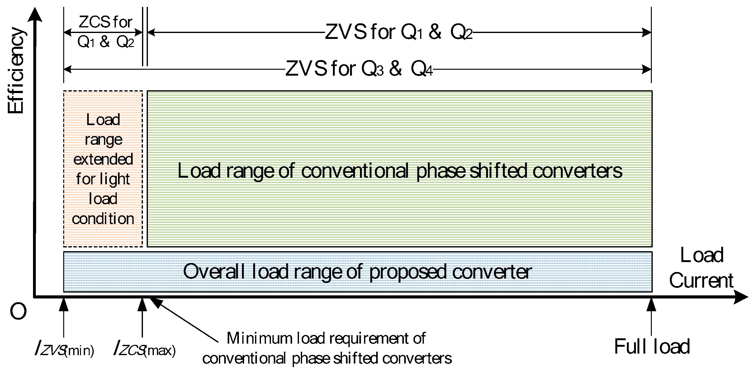
For the conventional converter, the efficiency will drop significantly at a light load condition as a result of the failure of active switches to achieve ZVS. This is why resonant converters including phase-shifted topology will be more favorable for high power applications. Besides, the operation of the conventional phase-shifted converter at light load may not only have a lower efficiency, but also generate excess heat loss that will definitely impair the lifetime of electronic components, and the converter may in some cases crash due to overheating. With the proposed technology, the active switches of the converter losing ZVS are now able to perform ZCS instead in case the load current is larger than IZVS(min) in Equation (37), which can minimize the switching loss and improve the overall efficiency.
Figure 7 shows a diagram indicating the extended load range for the bi-directional phase-shifted converter using the proposed control method. The extension of load range is from IZVS(min) to IZCS(max), while there is still a narrow region where the active switches cannot perform either ZVS or ZCS as explained in Figure 7, which can be eliminated by designing the minimum load of the conventional phase-shifted converter to be the same as IZCS(max).
4. Experimental Results
To verify the theory developed for the proposed control method, two experiments were set up for a performance test. The first one tested a conventional bi-directional phase-shifted converter, which employs a conventional control algorithm, and the second one tested the improved converter using the new control method. These two converters were constructed with an identical configuration, as shown in Table 3.
The experimental prototype is shown in Figure 8. The improved converter and conventional converter share the same primary side as the topology and all parameters are the same. The switching device in both the primary side and the secondary side of the improved converter is C2M0080120D Silicon Carbide MOSFET (Wolfspeed, Durham, NC, USA) with a maximum Drain-Source voltage of 1200 V and continuous Drain current of 31 A. The rectifier diodes and anti-parallel diodes in both converters are VS-3-EPH03PBF (Vishay Intertechnology, Malvern, PA, USA). A DSP28335 (Texas Instruments, Dallas, TX, USA) module generates the gate signals for the eight switches by ports GPIO0-GPIO7. The resonant capacitor in the primary side is a 310 V polypropylene capacitor. The output filter capacitor of the secondary side is a 450 V aluminium electrolytic capacitor. The transformer has five primary turns and 10 secondary turns, and the diameter of the insulated copper wire is 0.5 mm to reduce the skin effect in switching at 50 kHz. For the primary side and secondary side of the improved converter, the switches use heatsink at the bottom of the Printed Circuit Board (PCB). For the secondary side of the conventional converter, there are only rectifier diodes with TO-247 heatsink above the PCB.
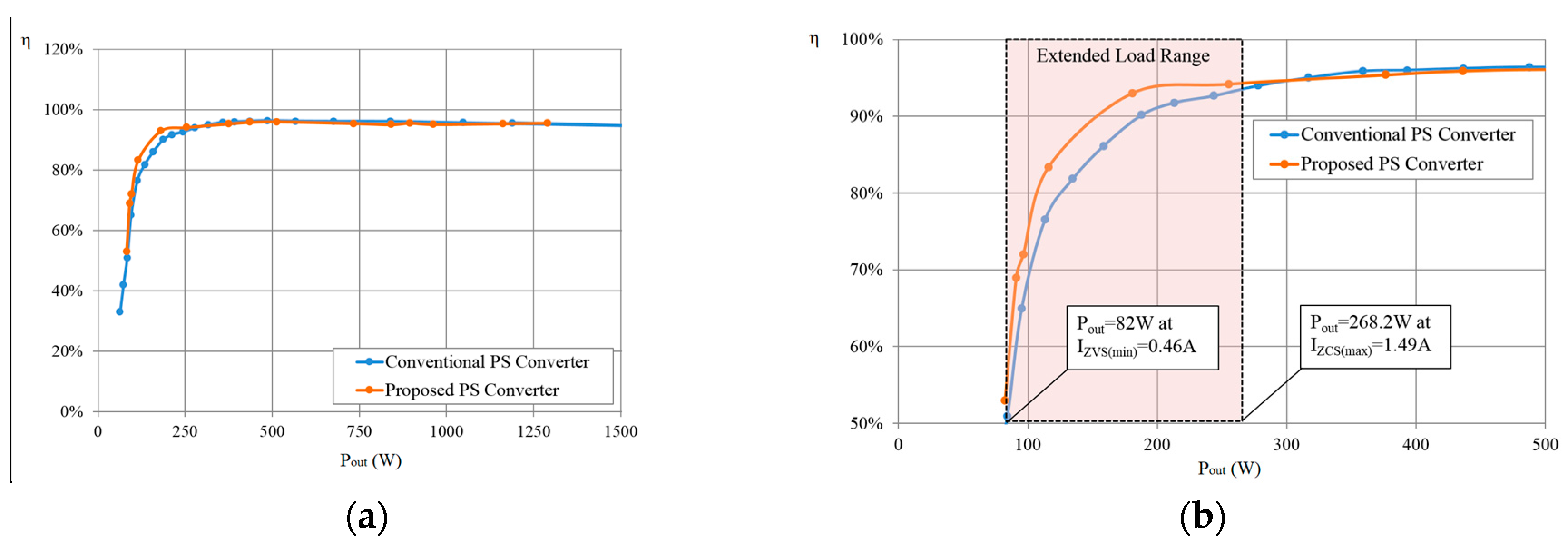
The efficiency of the two converters over the designed load range is plotted in Figure 9, where the range for full load and light load are illustrated in Figure 9a,b, respectively. The Y axis represents the efficiency η, and the X axis represents the output power Pout.
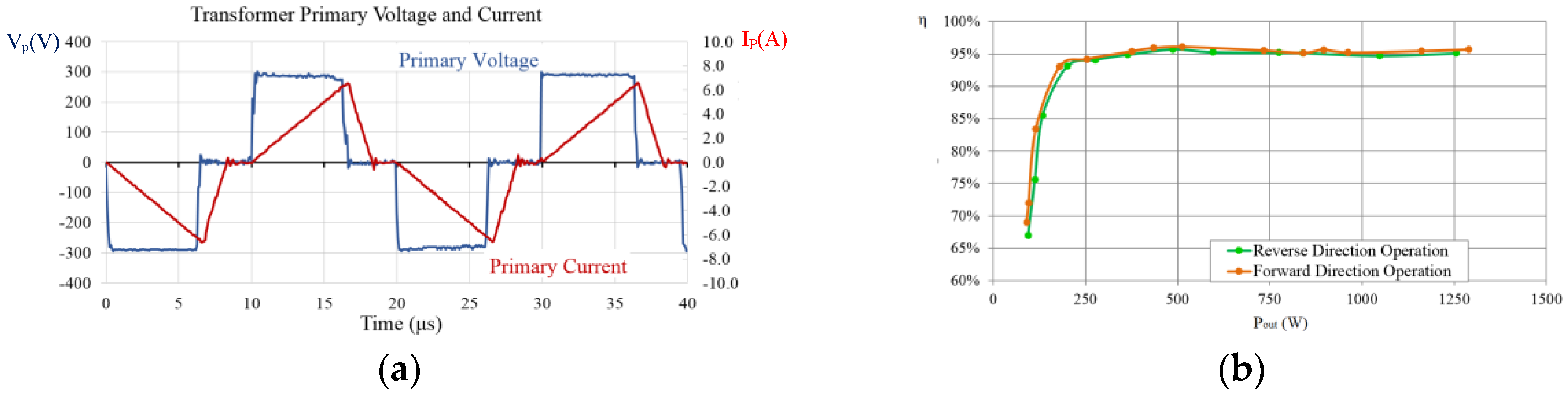
The maximum load current IZCS(max) for ZCS can be calculated using Equation (32) as 1.49 A, and the corresponding output power is 268.2 W, which is the boundary of the extended load range. Both of the converters achieve an average efficiency of 95% over the designed load range; however, as shown in Figure 9b, the improved converter operating within the extended load range has a higher efficiency than the conventional converter by 4–8%. Also, the minimum load current IZVS(min) for ZVS can be worked out using Equation(37) as 0.46 A, and the corresponding output power is 82 W. The converter efficiency will drop significantly below this power level. When the output power is higher than 268.2 W, the efficiency of the conventional converters and proposed converters is basically the same as they exhibit a similar performance during soft switching with sufficient energy stored in the resonant inductor.
Figure 10 illustrates the switching performance of the improved converter at an output power of 115 W, which lies in the light load region. The ZCS and ZVS are perfectly accomplished by Q2 at the left leg and Q4 at the right leg of the inverter bridge, as illustrated in Figure 10a,b, respectively, where the blue line shows the Drain-Source voltage and the red line represents the Drain current. In Figure 10a, Q2 switches on under zero current at t = 0 µs. In Figure 10b, Q4 switches on under zero voltage at t = 6 µs when the drain-source voltage of MOSFET reaches 0 V. The green line at the bottom shows the gate signal voltage of Q2 and Q4, respectively. The primary current and voltage of the transformer in Figure 10c,d agree well with the proposed theory, as illustrated in Figure 2.
The above experiment also demonstrated the capability of a bi-directional operation. As shown in Figure 1, the topology is symmetrical, except for the position of the resonant inductor Lres. Whether the inductor Lres locates in the primary side or secondary side of the transformer does not affect the converter’s operation because it is the same in the equivalent circuits, as shown in Figure 4b. The only difference is whether the inductance is referred to the primary side or secondary side of the transformer in the calculation, but the result is the same. Thus the converter could operate in the opposite direction by the same control scheme, including light load cases.
The transformer’s turn ratio is 1:2 in the prototype, so it is a step-up converter. If the converter is used in the reverse direction, the turn ratio becomes 2:1, and is thus a step-down converter. Therefore, in the experiment of the reverse direction operation, the input voltage is set to 300 Vdc and the designated output voltage is 120 V. The control scheme is unchanged, and the experimental results are presented in Figure 11. The converter works well and the waveforms of primary voltage and current are the same, as illustrated in Figure 2. The efficiency of the reverse direction operation is satisfactory and higher than 95% in the normal load range, though it is slightly lower than in the forward direction operation as the turn ratio, input and output voltage, minimum load current to achieve ZVS, and average current passing through the switches are all different, even for the same output power level in the forward and backward direction.
5. Conclusions
A new control method for the bi-directional phase-shift-controlled DC-DC converter is proposed that can provide a path for reverse power flow and an extended load range for a light load condition. The proposed control method incorporates the gate drive logic for synchronous rectification to further improve the overall performance of the converter. The control method is built on a mathematical model to ensure that soft switching can be realized, especially at a light load condition. The proposed control method also has the advantage of giving the converter a linear output voltage relationship with the phase shift. Coupled with the fast dynamic response characteristics, the proposed converter is particularly suitable for applications such as energy recovery from unsteady sources which fluctuate dramatically. An experimental prototype of a 1.5 kW DC-DC converter with the proposed control method was built to demonstrate its capability of bi-directional power flow and show the higher conversion efficiency, especially at light load, compared to the conventional phase-shifted converter.
Acknowledgments
This work was supported by the Innovation and Technology Commission of the HKSAR Government to the Hong Kong Branch of National Rail Transit Electrification and Automation Engineering Technology Research Center under Grant Nos. 1-BBYW and 1-BBYF. The support by The Hong Kong Polytechnic University under Projects 4-ZZEX and RUB1 is also acknowledged.
Author Contributions
Wenzheng Xu and Nelson Hon Lung Chan proposed the control methods and the mathematical analysis; Wenzheng Xu designed and conducted the simulation and experiments, as well as prepared the paper; Siu Wing Or and Siu Lau Ho analyzed the simulation and experimental results; Ka Wing Chan provided the experimental platform and optimized the design.
Conflicts of Interest
The authors declare no conflict of interest.
References
- Iannuzzi, D.; Pagano, E.; Tricoli, P. The Use of Energy Storage Systems for Supporting the Voltage Needs of Urban and Suburban Railway Contact Lines. Energies 2013, 6, 1802–1820. [Google Scholar] [CrossRef]
- Li, Y.; Mai, R.; Lin, T.; Sun, H.; He, Z. A Novel WPT System Based on Dual Transmitters and Dual Receivers for High Power Applications: Analysis, Design and Implementation. Energies 2017, 10, 174. [Google Scholar] [CrossRef]
- Arango, E.; Ramos-Paja, C.A.; Calvente, J.; Giral, R.; Serna, S. Asymmetrical Interleaved DC/DC Switching Converters for Photovoltaic and Fuel Cell Applications—Part 1: Circuit Generation, Analysis and Design. Energies 2012, 5, 4590–4623. [Google Scholar] [CrossRef]
- Aryani, D.R.; Song, H. Coordination Control Strategy for AC/DC Hybrid Microgrids in Stand-Alone Mode. Energies 2016, 9, 469. [Google Scholar] [CrossRef]
- He, X.; Guo, A.; Peng, X.; Zhou, Y.; Shi, Z.; Shu, Z. A Traction Three-Phase to Single-Phase Cascade Converter Substation in an Advanced Traction Power Supply System. Energies 2015, 8, 9915–9929. [Google Scholar] [CrossRef]
- Baars, N.H.; Everts, J.; Huisman, H.; Duarte, J.L.; Lomonova, E.A. A 80-kW Isolated DC-DC Converter for Railway Applications. IEEE Trans. Power Electron. 2015, 30, 6639–6647. [Google Scholar] [CrossRef]
- Wang, C.; Li, W.; Wang, Y.; Han, F.Q.; Chen, B. A High-Efficiency Isolated LCLC Multi-Resonant Three-Port Bidirectional DC-DC Converter. Energies 2017, 10, 934. [Google Scholar] [CrossRef]
- Jiang, J.; Bao, Y.; Wang, L. Topology of a Bidirectional Converter for Energy Interaction between Electric Vehicles and the Grid. Energies 2014, 7, 4858–4894. [Google Scholar] [CrossRef]
- Lu, X.; Wan, J. Modeling and Control of the Distributed Power Converters in a Standalone DC Microgrid. Energies 2016, 9, 217. [Google Scholar] [CrossRef]
- Song, W.; Ma, J.; Zhou, L.; Feng, X. Deadbeat Predictive Power Control of Single-Phase Three-Level Neutral-Point-Clamped Converters Using Space-Vector Modulation for Electric Railway Traction. IEEE Trans. Power Electron. 2016, 31, 721–732. [Google Scholar] [CrossRef]
- Wang, S.; Song, W.; Zhao, J.; Feng, X. Hybrid single-carrier-based pulse width modulation scheme for single-phase three-level neutral-point-clamped grid-side converters in electric railway traction. IET Power Electron. 2016, 9, 2500–2509. [Google Scholar] [CrossRef]
- Sharifi, D.; Tricoli, P.; Hillmansen, S. A new control technique enabling dual-feeding of 50 Hz AC railways with static converter feeder stations. In Proceedings of the 8th IET International Conference on Power Electronics, Machines and Drives (PEMD 2016), Glasgow, UK, 19–21 April 2016. [Google Scholar]
- Lai, C.; Yang, M.; Liang, S. A Zero Input Current Ripple ZVS/ZCS Boost Converter with Boundary-Mode Control. Energies 2014, 7, 6765–6782. [Google Scholar] [CrossRef]
- Zhao, L.; Li, H.; Yu, Y.; Wang, Y. A Novel Choice Procedure of Magnetic Component Values for Phase Shifted Full Bridge Converters with a Variable Dead-Time Control Method. Energies 2015, 8, 9655–9669. [Google Scholar] [CrossRef]
- Liu, K.B.; Liu, C.Y.; Liu, Y.H.; Chien, Y.C.; Wang, B.S.; Wong, Y.S. Analysis and Controller Design of a Universal Bidirectional DC-DC Converter. Energies 2016, 9, 501. [Google Scholar] [CrossRef]
- Jauch, F.; Biela, J. Combined Phase Shift and Frequency Modulation of a Dual Active Bridge AC-DC Converter with PFC. IEEE Trans. Power Electron. 2016, 31, 8387–8397. [Google Scholar] [CrossRef]
- Lai, Y.S.; Su, Z.J.; Chang, Y.T. Novel Phase-Shift Control Technique for Full-Bridge Converter to Reduce Thermal Imbalance under Light-Load Condition. IEEE Trans. Ind. Appl. 2015, 51, 1651–1659. [Google Scholar] [CrossRef]
- Kim, J.W.; Kim, D.Y.; Kim, C.E.; Moon, G.W. A simple switching control technique for improving light load efficiency in a phase-shifted full-bridge converter with a server power system. IEEE Trans. Power Electron. 2014, 29, 1562–1566. [Google Scholar] [CrossRef]
- Kim, J.H.; Kim, C.E.; Kim, J.K.; Lee, J.B.; Moon, G.W. Analysis on Load-Adaptive Phase-Shift Control for High Efficiency Full-Bridge LLC Resonant Converter under Light-Load Conditions. IEEE Trans. Power Electron. 2016, 31, 4942–4955. [Google Scholar]
- Chen, B.-Y.; Lai, Y. Switching control technique of phase-shift-controlled full-bridge converter to improve efficiency under light-load and standby conditions without additional auxiliary components. IEEE Trans. Power Electron. 2010, 25, 1001–1012. [Google Scholar] [CrossRef]
- Zhao, L.; Xu, C.; Zheng, X.; Li, H. A Dual Half-Bridge Converter with Adaptive Energy Storage to Achieve ZVS over Full Range of Operation Conditions. Energies 2017, 10, 444. [Google Scholar] [CrossRef]
- Pandey, R.; Tripathi, R.N.; Hanamoto, T. Comprehensive Analysis of LCL Filter Interfaced Cascaded H-Bridge Multilevel Inverter-Based DSTATCOM. Energies 2017, 10, 346. [Google Scholar] [CrossRef]
- Lai, Y.-S.; Su, Z. New Integrated Control Technique for Two-Stage Server Power to Improve Efficiency under the Light-Load Condition. IEEE Trans. Ind. Electron. 2015, 62, 6944–6954. [Google Scholar] [CrossRef]
- Wang, C.S.; Li, W.; Wang, Y.F.; Han, F.Q.; Meng, Z.; Li, G.D. An Isolated Three-Port Bidirectional DC-DC Converter with Enlarged ZVS Region for HESS Applications in DC Microgrids. Energies 2017, 10, 446. [Google Scholar] [CrossRef]
- Zhao, L.; Li, H.; Hou, Y.; Yu, Y. Operation analysis of a phase-shifted full-bridge converter during the dead-time interval. IET Power Electron. 2016, 9, 1777–1783. [Google Scholar] [CrossRef]
- Ting, Y.; de Haan, S.; Ferreira, J.A. DC-DC Full-Bridge Hybrid Series Resonant Converter enabling constant switching frequency across wide load range. In Proceedings of the 7th International Power Electronics and Motion Control Conference, Harbin, China, 2 June 2012. [Google Scholar]
- Kim, Y.D.; Cho, K.M.; Kim, D.Y.; Moon, G.W. Wide-range ZVS phase-shift full-bridge converter with reduced conduction loss caused by circulating current. IEEE Trans. Power Electron. 2013, 23, 3308–3316. [Google Scholar] [CrossRef]
- Sekar, A.; Raghavan, D. Implementation of Single Phase Soft Switched PFC Converter for Plug-in-Hybrid Electric Vehicles. Energies 2015, 8, 13096–13111. [Google Scholar] [CrossRef]
- Lee, I.O.; Moon, G.W. Analysis and design of phase-shifted dual H-bridge converter with a wide ZVS range and reduced output filter. IEEE Trans. Ind. Electron. 2013, 60, 4415–4426. [Google Scholar] [CrossRef]
- Shi, X.; Jiang, J.; Guo, X. An Efficiency-Optimized Isolated Bidirectional DC-DC Converter with Extended Power Range for Energy Storage Systems in Microgrids. Energies 2013, 6, 27–44. [Google Scholar] [CrossRef]
- Cho, J.G.; Baek, J.W.; Jeong, C.Y.; Yoo, D.W.; Joe, K.Y. Novel Zero-Voltage and Zero-Current-Switching Full Bridge PWM Converter Using Transformer Auxiliary Winding. IEEE Trans. Power Electron. 2000, 15, 250–257. [Google Scholar]
- Tsai, C.T.; Shen, C.L.; Su, J.C. A Power Supply System with ZVS and Current-Doubler Features for Hybrid Renewable Energy Conversion. Energies 2013, 6, 4859–4878. [Google Scholar] [CrossRef]
- Cho, J.G.; Sabate, J.A.; Hua, G.; Lee, F.C. Zero-Voltage and Zero-Current-Switching Full Bridge PWM Converter for High-Power Applications. IEEE Trans. Power Electron. 1996, 11, 622–628. [Google Scholar]
- Ruan, X.; Li, B. Zero-voltage and zero-current-switching PWM hybrid full-bridge three-level converter. IEEE Trans. Ind. Electron. 2005, 52, 213–220. [Google Scholar] [CrossRef]
- Shen, Y.; Sun, X.; Li, W.; Wu, X.; Wang, B. A Modified Dual Active Bridge Converter with Hybrid Phase-Shift Control for Wide Input Voltage Range. IEEE Trans. Power Electron. 2016, 31, 6884–6900. [Google Scholar] [CrossRef]
- Meng, Z.; Wang, Y.; Yang, L.; Li, W. Analysis of Power Loss and Improved Simulation Method of a High Frequency Dual-Buck Full-Bridge Inverter. Energies 2017, 10, 311. [Google Scholar] [CrossRef]
Figure 1.
(a) Topology of the Bi-directional Phase-Shift-Controlled DC-DC Converter; (b) Topology of a Conventional Phase-Shifted Converter.
Figure 1.
(a) Topology of the Bi-directional Phase-Shift-Controlled DC-DC Converter; (b) Topology of a Conventional Phase-Shifted Converter.
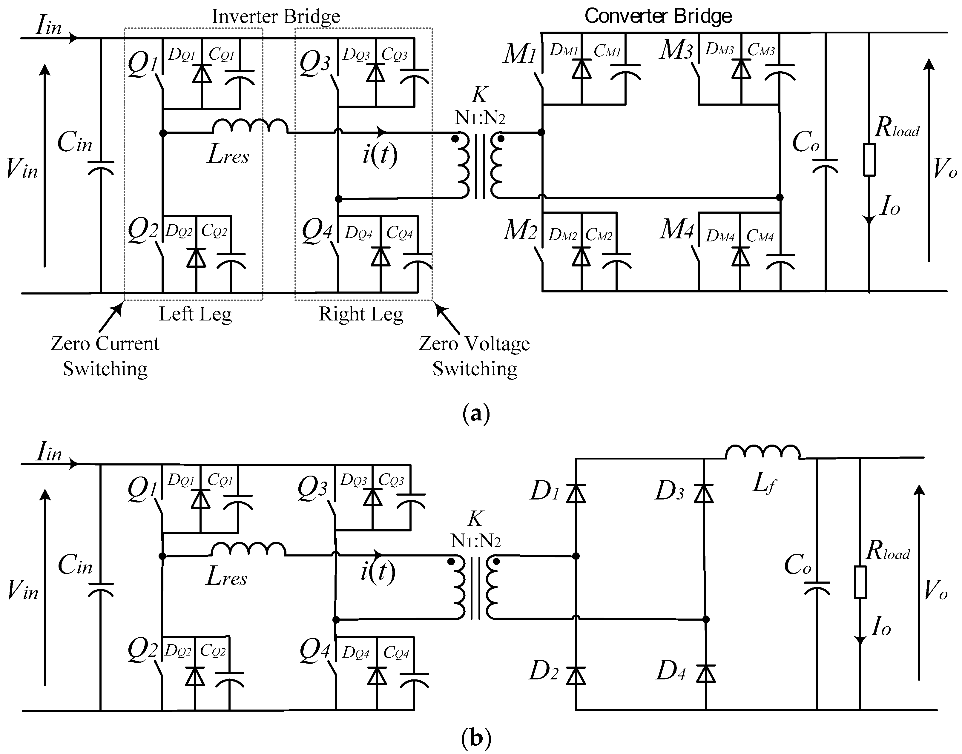
Figure 2.
Gate Drive Signals of Proposed Control Method.

Figure 3.
Power flow of operation: (a) Mode 1—Dead time; (b) Mode 2—ZCS; (c) Mode 3—Power transferring; (d) Mode 4—ZVS; (e) Mode 5—Freewheeling; (f) Mode 6—Nil.
Figure 3.
Power flow of operation: (a) Mode 1—Dead time; (b) Mode 2—ZCS; (c) Mode 3—Power transferring; (d) Mode 4—ZVS; (e) Mode 5—Freewheeling; (f) Mode 6—Nil.

Figure 4.
Input Energy During Power Transferring Stage: (a) Primary Voltage and Current; (b) Equivalent circuit.
Figure 4.
Input Energy During Power Transferring Stage: (a) Primary Voltage and Current; (b) Equivalent circuit.
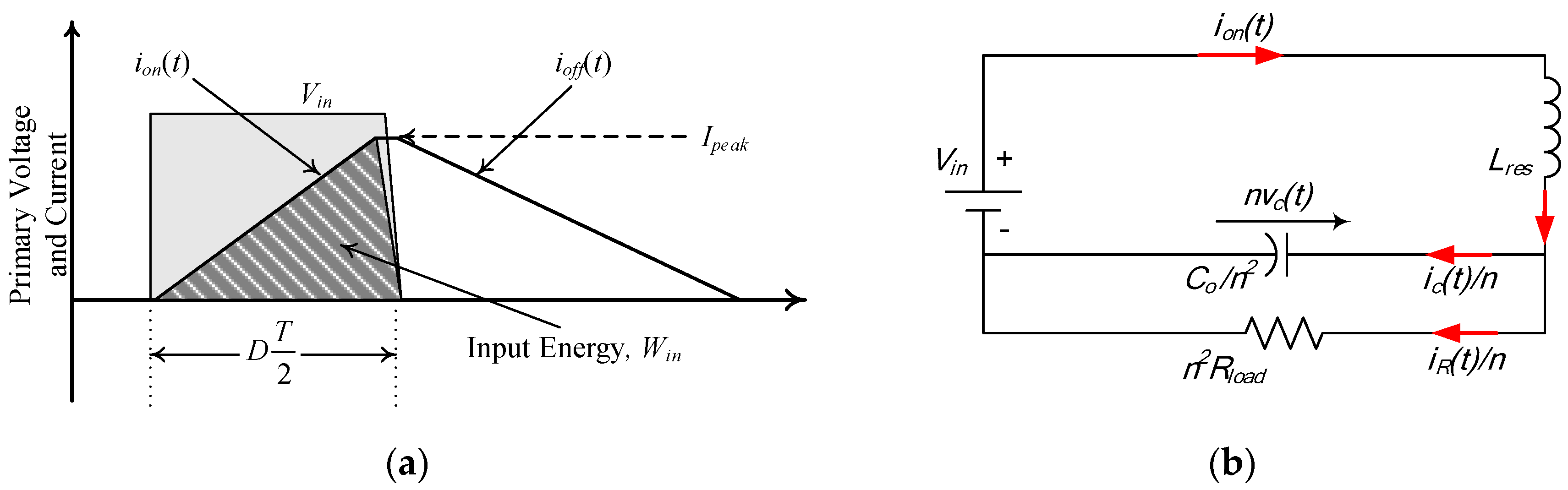
Figure 5.
Load Current for ZCS and ZVS: (a) ZCS; (b) Marginal ZCS; (c) Neither ZCS nor ZVS; (d) Marginal ZVS.
Figure 5.
Load Current for ZCS and ZVS: (a) ZCS; (b) Marginal ZCS; (c) Neither ZCS nor ZVS; (d) Marginal ZVS.
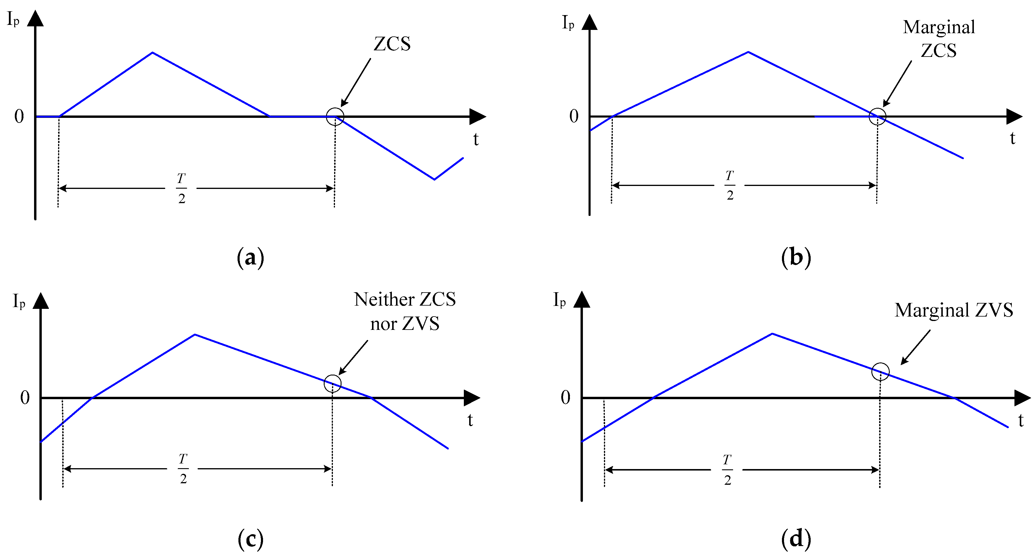
Figure 6.
Equivalent Circuit of the Freewheeling Stage.

Figure 7.
Diagram of Extended Load Range.

Figure 8.
Experimental prototype with a rated power of 1.5 kW.
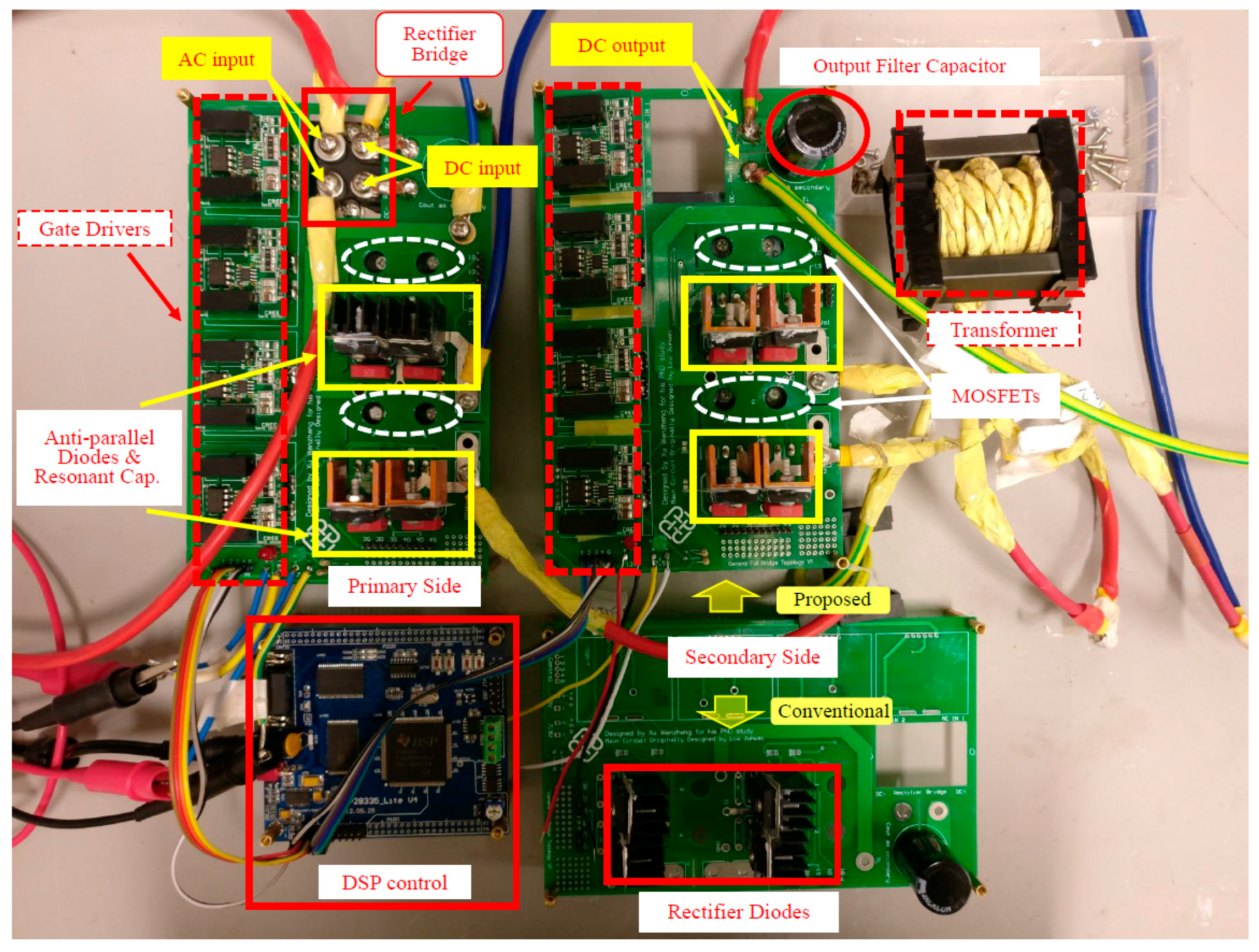
Figure 9.
Efficiency and Load Range: (a) Conversion Efficiency of Full Load Range; (b) Conversion Efficiency of Light Load Range.
Figure 9.
Efficiency and Load Range: (a) Conversion Efficiency of Full Load Range; (b) Conversion Efficiency of Light Load Range.

Figure 10.
Switching Performance of Improved Converter: (a) Q2 Switching under Zero Current Condition; (b) Q4 Switching under Zero Voltage Condition; (c) Transformer Primary Voltage and Current at Light Load; (d) Transformer Primary Voltage and Current at Full Load.
Figure 10.
Switching Performance of Improved Converter: (a) Q2 Switching under Zero Current Condition; (b) Q4 Switching under Zero Voltage Condition; (c) Transformer Primary Voltage and Current at Light Load; (d) Transformer Primary Voltage and Current at Full Load.
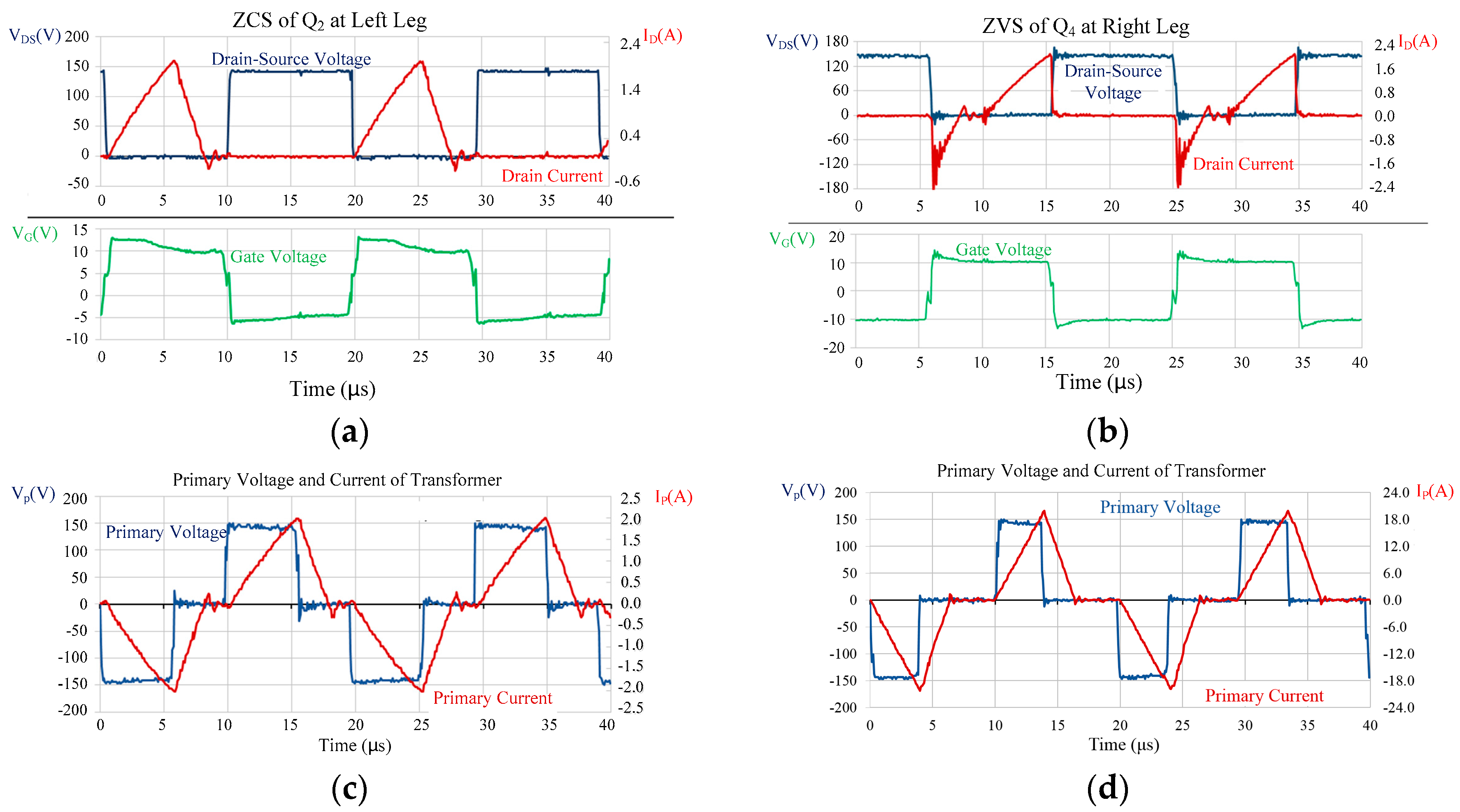
Figure 11.
Bi-directional Operation Experiment (a) Transformer Primary Voltage and Current of Reverse Direction Operation; (b) Efficiency comparison.
Figure 11.
Bi-directional Operation Experiment (a) Transformer Primary Voltage and Current of Reverse Direction Operation; (b) Efficiency comparison.

Table 1.
Definition of common terms used.
| Symbol | Definition | Equation |
|---|---|---|
| D | Phase shift of gate signals between left and right leg | - |
| n | Turn ratio of transformer | N1/N2 |
| fs | Switching frequency | 1/T |
| T | Period of switching cycle | - |
| ωs | Angular switching frequency | 2 π fs |
| ωo | Output resonant frequency | |
| Zo | Characteristic impedance | |
| Zn | Normalized load resistance |
Table 2.
Definition of common equations used.
| Equations | Definition |
|---|---|
| ion(t) | primary current of transformer |
| iR(t)/n | primary referred secondary current of transformer |
| iC(t)/n | primary referred secondary current of output capacitor |
| nvc(t) | primary referred secondary output voltage of converter |
| n2Rload | primary referred secondary load resistance |
| C/n2 | primary referred secondary output filter capacitance |
Table 3.
Parameters of the two converters for the performance test.
| Items | Value |
|---|---|
| Input voltage, Vin | 150 V |
| Output voltage, Vo | 180 V |
| Output power, Po | 60 W–1500 W |
| Turn ratio, n | 1:2 |
| Resonant inductance, Lres | 1 µH |
| Resonant capacitance, CQ1–4 | 4.7 nF |
| Output capacitor, Co | 60 µF |
| Switching frequency, fs | 50 kHz |
© 2017 by the authors. Licensee MDPI, Basel, Switzerland. This article is an open access article distributed under the terms and conditions of the Creative Commons Attribution (CC BY) license (http://creativecommons.org/licenses/by/4.0/).
Share and Cite
MDPI and ACS Style
Xu, W.; Chan, N.H.L.; Or, S.W.; Ho, S.L.; Chan, K.W. A New Control Method for a Bi-Directional Phase-Shift-Controlled DC-DC Converter with an Extended Load Range. Energies 2017, 10, 1532. https://doi.org/10.3390/en10101532
AMA Style
Xu W, Chan NHL, Or SW, Ho SL, Chan KW. A New Control Method for a Bi-Directional Phase-Shift-Controlled DC-DC Converter with an Extended Load Range. Energies. 2017; 10(10):1532. https://doi.org/10.3390/en10101532
Chicago/Turabian StyleXu, Wenzheng, Nelson Hon Lung Chan, Siu Wing Or, Siu Lau Ho, and Ka Wing Chan. 2017. "A New Control Method for a Bi-Directional Phase-Shift-Controlled DC-DC Converter with an Extended Load Range" Energies 10, no. 10: 1532. https://doi.org/10.3390/en10101532
Note that from the first issue of 2016, this journal uses article numbers instead of page numbers. See further details here.